

Page 1
FEATURES
OUTPUT CURRENT (mA)
0
OUTPUT VOLTAGE (V)
8.5
9.0
8.9
8.8
8.7
8.6
9.5
9.4
9.3
9.2
9.1
50 100
1425 TA02
150 200
■
No Transformer “Third Winding” or Optoisolator
Required
■
±5% Accurate Output Voltage Without User Trims
(See Circuit Below)
■
Resistor Programmable Output Voltage
■
Regulation Maintained Well Into Discontinuous
Mode (Light Load)
■
Optional Load Compensation
■
Operating Frequency: 285kHz
■
Easily Synchronized to External Clock
■
Available in 16-Pin Narrow SO Package
U
APPLICATIONS
■
Isolated Flyback Switching Regulators
■
Ethernet Isolated 5V to –9V Converters
■
Medical Instruments
■
Isolated Telecom Supplies
, LTC and LT are registered trademarks of Linear Technology Corporation.
LT1425
Isolated Flyback
Switching Regulator
U
DESCRIPTION
The LT®1425 is a monolithic high power switching regulator specifically designed for the isolated flyback topology. No “third winding” or optoisolator is required; the
integrated circuit senses the isolated output voltage
directly from the primary side flyback waveform. A high
current, high efficiency switch is included on the die along
with all oscillator, control and protection circuitry.
The LT1425 operates with input supply voltages from 3V
to 20V and draws only 7mA quiescent current. It can
deliver output power up to 6W with no external power
devices. By utilizing current mode switching techniques, it
provides excellent AC and DC line regulation.
The LT1425 has a number of features not found on other
switching regulator ICs. Its unique control circuitry can
maintain regulation well into discontinuous mode in most
applications. Optional load compensation circuitry allows
for improved load regulation. An externally activated shutdown mode reduces total supply current to 15µA for
standby operation.
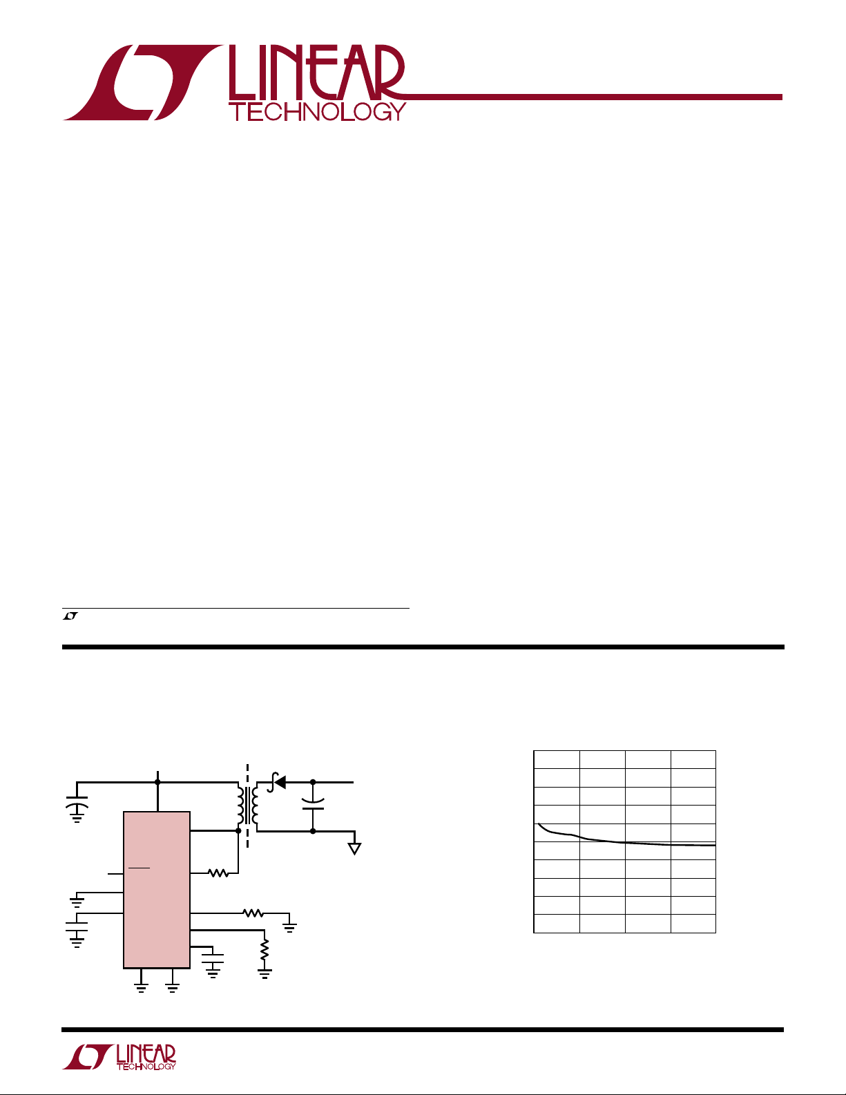
TYPICAL APPLICATION
+
C1
100µF
10V
C3
1000pF
15
SHDN
6
SYNC
4
V
C
SGND PGND
5V to Isolated –9V
5V
12
V
IN
11
V
SW
LT1425
710
R
FB
R
REF
R
OCOMP
R
CCOMP
3
5
14
13
500V
ISOLATION BARRIER
T1*
D1
1N5819
••
R1
22.6k
1%
*DALE LPE 4841-330MB
R2
3.01k
1%
C4
0.1µF
R3
15k
U
OUT
C2
47µF
+
16V
1425 TA01
–
V
ISOLATED
–9V ±5% AT
20mA TO 200mA
F
Load Regulation
1
Page 2

LT1425
WW
W
ABSOLUTE MAXIMUM RATINGS
U
U
W
PACKAGE/ORDER INFORMATION
(Note 1)
Supply Voltage ........................................................ 20V
Switch Voltage......................................................... 35V
SHDN, SYNC Pin Voltage........................................... 7V
RFB Pin Current....................................................... 2mA
Operating Junction Temperature Range
Commercial .......................................... 0°C to 100°C
Industrial ......................................... – 40°C to 100°C
Storage Temperature Range ................. –65°C to 150°C
Lead Temperature (Soldering, 10 sec).................. 300°C
1
GND
2
NC
3
R
FB
4
V
C
5
R
REF
6
SYNC
7
SGND
8
GND
16-LEAD PLASTIC SO
T
JMAX
TOP VIEW
16
15
14
13
12
11
10
9
S PACKAGE
= 145°C, θJA = 75°C/ W
GND
SHDN
R
OCOMP
R
CCOMP
V
IN
V
SW
PGND
GND
ORDER PART
NUMBER
LT1425CS
LT1425IS
Consult factory for Military grade parts.
ELECTRICAL CHARACTERISTICS
SYMBOL PARAMETER CONDITIONS MIN TYP MAX UNITS
Feedback Amplifier
I
REF
I
IN
g
m
I
SOURCE
V
CL
Output Switch
BV Output Switch Breakdown Voltage IC = 5mA ● 35 50 V
V(VSW) Output Switch ON Voltage ISW = 1A ● 0.55 0.85 V
I
LIM
Current Amplifier
Timing
f Switching Frequency 260 285 300 kHz
t
ON
t
ED
t
EN
Reference Current Measured at RFB Pin with R
R
Pin Input Current 500 nA
REF
Feedback Amplifier Transconductance ∆IC = ±10µA (Note 2) ● 400 1000 1600 µmho
, I
Feedback Amplifier Source or Sink Current ● 30 50 80 µA
SINK
Feedback Amplifier Clamp Voltage 1.9 V
Reference Voltage/Current Line Regulation 5V ≤ VIN ≤ 18V ● 0.01 0.04 %/V
Voltage Gain (Note 3) 500 V/V
VIN Sense Error ● 10 25 mV
Switch Current Limit Duty Cycle = 50%, 0°C ≤ TJ ≤ 100°C ● 1.35 1.60 1.9 A
Control Pin Threshold Duty Cycle = Minimum 0.95 1.2 1.3 V
Control Voltage to Switch Transconductance 2 A/V
Minimum Switch ON Time 170 210 260 ns
Flyback Enable Delay Time 150 ns
Minimum Flyback Enable Time 180 ns
Maximum Switch Duty Cycle ● 85 90 95 %
VIN = 5V, TJ = 25°C, VSW open, VC = 1.4V, unless otherwise specified.
= 3.000k 402 408 414 µA
REF
Duty Cycle = 50%, –40°C ≤ T
Duty Cycle = 80% 1.30 A
≤ 100°C ● 1.25 1.60 1.9 A
J
● 396 420 µA
● 0.85 1.4 V
● 240 320 kHz
U
2
Page 3
LT1425
ELECTRICAL CHARACTERISTICS
VIN = 5V, TJ = 25°C, VSW Open, VC = 1.4V, unless otherwise specified.
SYMBOL PARAMETER CONDITIONS MIN TYP MAX UNITS
Load Compensation
∆V
RCCOMP
/∆I
SW
0.45 Ω
SYNC Function
Minimum SYNC Amplitude ● 1.5 2.2 V
Synchronization Range 320 450 kHz
SYNC Pin Input Resistance 40 kΩ
Power Supply
V
IN(MIN)
I
CC
Minimum Input Voltage ● 2.8 3.1 V
Supply Current ● 7.0 9.5 mA
Shutdown Mode Supply Current ● 15 40 µA
Shutdown Mode Threshold ● 0.4 0.9 1.3 V
The ● denotes the specifications which apply over the full operating
temperature range.
Note 2: Feedback amplifier transconductance is R
Note 3: Voltage gain is R
referred.
REF
referred.
REF
Note 1: Absolute Maximum Ratings are those values beyond which the life
of a device may be impaired.
UW
TYPICAL PERFORMANCE CHARACTERISTICS
Switch Saturation Voltage vs
Switch Current
1.2
1.0
0.8
0.6
0.4
0.2
SWITCH SATURATION VOLTAGE (V)
0
0
0.2 0.4
SWITCH CURRENT (A)
0.8 1.2 1.4
0.6 1.0
125°C
25°C
–55°C
1425 G01
Switch Current Limit vs
Duty Cycle
2.0
TA = 25°C
1.5
1.0
0.5
SWITCH CURRENT LIMIT (A)
0
102030
0
40
DUTY CYCLE (%)
50 60 70 80 90 100
1425 G02
Minimum Input Voltage vs
Temperature
3.1
3.0
2.9
2.8
2.7
INPUT VOLTAGE (V)
2.6
2.5
2.4
–50
–25 0
TEMPERATURE (°C)
50 100 125
25 75
1425 G03
3
Page 4

LT1425
UW
TYPICAL PERFORMANCE CHARACTERISTICS
Feedback Amplifier Output
60
40
20
0
–20
–40
–60
FEEDBACK AMPLIFIER OUTPUT CURRENT (µA)
–80
1.05
Current vs R
1.10 1.15
REF
1.20 1.30
R
NODE VOLTAGE (V)
REF
Switching Frequency vs
Temperature
300
295
290
285
280
275
SWITCHING FREQUENCY (kHz)
270
Pin Voltage
25°C
125°C
–55°C
1.25 1.35 1.40
1425 G04
Error Amplifier Transconductance
vs Temperature (R
1400
1200
1000
800
600
400
TRANSCONDUCTANCE (µmho)
200
0
–50
–25 0
TEMPERATURE (°C)
REF
50 100 125
25 75
Minimum Synchronization
Voltage vs Temperature
)
2.50
P-P
2.25
2.00
1.75
1.50
1.25
1.00
Referred)
1425 G05
VC Pin Threshold and High Clamp
Voltage vs Temperature
2.50
2.25
2.00
1.75
1.50
PIN VOLTAGE (V)
C
V
1.25
1.00
0.75
–50
–25 0
VC HIGH CLAMP
VC THRESHOLD
50 100 125
25 75
TEMPERATURE (°C)
SHDN Pin Input Current vs
Voltage
1
TA = 25°C
0
–1
–2
–3
SHDN PIN INPUT CURRENT (µA)
1425 G06
265
–50
–25 0
25 75
TEMPERATURE (°C)
Minimum Switch ON Time vs
Temperature
300
275
250
225
200
175
SWITCH ON TIME (ns)
150
125
–50
–25 0
25 75
TEMPERATURE (°C)
4
50 100 125
1425 G07
50 100 125
1425 G10
MINIMUM SYNCHRONIZATION VOLTAGE (V
0.75
–50
–25 0
TEMPERATURE (°C)
50 100 125
25 75
Flyback Enable Delay Time vs
Temperature
250
225
200
175
150
125
ENABLE DELAY TIME (ns)
100
75
–50
–25 0
TEMPERATURE (°C)
50 100 125
25 75
1425 G08
1425 G11
–4
1
0
SHDN PIN VOLTAGE (V)
3
2
Minimum Flyback Enable Time vs
Temperature
275
250
225
200
175
ENABLE TIME (ns)
150
125
100
–50
–25 0
TEMPERATURE (°C)
50 100 125
25 75
4
5
1425 G09
1425 G12
Page 5

PIN FUNCTIONS
LT1425
UUU
GND (Pins 1, 8, 9, 16): Ground. These pins connect to the
substrate of the die and are separate from the power
ground and signal ground. They should connect directly to
a good quality ground plane.
RFB (Pin 3): Input Pin for External “Feedback” Resistor
Connected to Transformer Primary (VSW). The ratio of this
resistor to the R
(VBG) reference, is the primary determinant of the output
voltage (plus the effect of any nonunity transformer turns
ratio). The average current through this resistor during the
flyback period should be approximately 400µ A. See Applications Information for more details.
VC (Pin 4): Control Voltage. This pin is the output of the
feedback amplifier and the input of the current comparator. Frequency compensation of the overall loop is effected
by placing a capacitor between this node and ground.
R
(Pin 5): Input Pin for External Ground-Referred
REF
“Reference” Resistor. This resistor should be in the range
of 3k, but for convenience, need not be this value precisely.
See Applications Information for more details.
SYNC (Pin 6): Pin to Synchronize Internal Oscillator to
External Frequency Reference. It is directly logic compatible and can be driven with any signal between 10% and
90% duty cycle. If unused, this pin can be left floating;
however, for best noise immunity the pin should be
grounded.
SGND (Pin 7): Signal Ground. This pin is a clean ground.
The internal reference and feedback amplifier are referred
to it. Keep the ground path connection to R
compensation capacitor free of large ground currents.
resistor, times the internal bandgap
REF
and the V
REF
C
PGND (Pin 10): Power Ground. This pin is the emitter of
the power switch device and has large currents flowing
through it. It should be connected directly to a good quality
ground plane.
VSW (Pin 11): This is the collector node of the output
switch and has large currents flowing through it. Keep the
traces to the switching components as short as possible
to minimize electromagnetic radiation and voltage spikes.
VIN (Pin 12): Supply Voltage. Bypass input supply pin with
10µ F or more. The part goes into undervoltage lockout
when VIN drops below 2.8V. Undervoltage lockout stops
switching and pulls the VC pin low.
R
Load Compensation Function. A common 0.1µF
ceramic capacitor will suffice for most applications. See
Applications Information for further details.
R
Compensation Resistor. Use of this pin allows nominal
compensation for nonzero output impedance in the power
transformer secondary circuit, including secondary winding impedance, output Schottky diode impedance and
output capacitor ESR. In less demanding applications this
resistor is not needed. See Applications Information for
more details.
SHDN (Pin 15): Shutdown. This pin is used to turn off the
regulator and reduce VIN input current to a few tens of
microamperes. The SHDN pin can be left floating when
unused.
(Pin 13): Pin for the External Filter Capacitor for
CCOMP
(Pin 14): Input Pin for Optional External Load
OCOMP
5
Page 6
LT1425
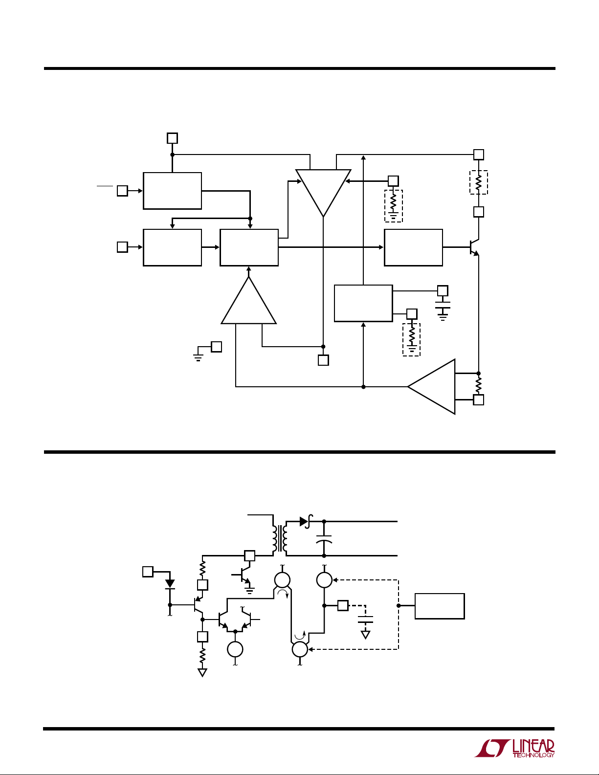
BLOCK DIAGRAM
V
W
IN
R
FB
R
REF
SHDN
SYNC
2.6V
REGULATOR
285kHz
OSCILLATOR
COMP
SGND
GND IS OMITTED FOR CLARITY
WW
FLYBACK ERROR A PLIFIER DIAGRA
FLYBACK
ERROR
AMPLIFIER
COMPENSATION
V
C
LOAD
DRIVERLOGIC
R
OC0MP
R
CCOMP
CURRENT
AMPLIFIER
V
SW
+
R
SENSE
–
PGND
1425 BD
6
V
IN
V
SW
V
IN
D2
R
FB
R
FB
Q1
Q2 Q3
R
REF
I
R
REF
•
Q4
V
BG
D1
T1
•
+
C1
+
ISOLATED
V
OUT
–
I
M
I
FXD
V
C
ENABLE
C
EXT
I
M
1425 EA
Page 7

WWU
TI I G DIAGRA
LT1425
VSW
VOLTAGE
V
GND
SWITCH
STATE
MINIMUM t
U
OPERATION
IN
OFF ON
ON
FLYBACK AMP
STATE
ENABLE DELAY
MINIMUM ENABLE TIME
V
FLBK
OFF ON
ENABLEDDISABLED DISABLED
0.80×
V
FLBK
COLLAPSE
DETECT
1425 TD
The LT1425 is a current mode switching regulator IC that
has been designed specifically for the isolated flyback
topology. The special problem normally encountered in
such circuits is that information relating to the output
voltage on the isolated secondary side of the transformer
must be communicated to the primary side in order to
maintain regulation. Historically, this has been done with
optoisolators or extra transformer windings. Optoisolator
circuits waste output power and the extra components
they require increase the cost and physical volume of the
power supply. Optoisolators can also exhibit trouble due
to limited dynamic response (temporal), nonlinearity,
unit-to-unit variation and aging over life. Circuits
employing extra transformer windings also exhibit deficiencies. The extra winding adds to the transformer’s
physical size and cost. Dynamic response is often
mediocre. There is usually no method for maintaining
load regulation versus load.
The LT1425 derives its information about the isolated
output voltage by examining the primary side flyback
pulse waveform. In this manner no optoisolator nor extra
transformer winding is required. This IC is a quantum
improvement over previous approaches because: target
output voltage is directly resistor-programmable, regulation is maintained well into discontinuous mode and
optional load compensation is available.
The Block Diagram shows an overall view of the system.
Many of the blocks are similar to those found in traditional designs including: internal bias regulator, oscillator, logic, current amplifier and comparator, driver and
output switch. The novel sections include a special
flyback error amplifier and a load compensation mechanism. Also, due to the special dynamic requirements of
flyback control, the logic system contains additional
functionality not found in conventional designs.
7
Page 8

LT1425
U
OPERATION
Within the dashed lines in the Block Diagram can be found
the R
resistors on the user-programmable LT1425. The capacitor connected to the R
The LT1425 operates much the same as traditional current
mode switchers, the major difference being a different
type of error amplifier which derives its feedback information from the flyback pulse. Due to space constraints, this
discussion will not reiterate the basics of current mode
switcher/controllers and isolated flyback converters. A
good source of information on these topics is LTC’s
Application Note 19.
ERROR AMPLIFIER—PSEUDO DC THEORY
Please refer to the simplified diagram of the Flyback Error
Amplifier. Operation is as follows: when output switch Q4
turns off, its collector voltage rises above the VIN rail. The
amplitude of this flyback pulse, i.e., the difference between
it and VIN, is given as:
, RFB and R
REF
resistors. They are external
OCOMP
pin is also external.
CCOMP
V
FLBK
α
R
FB
V
FLBK
α = Ratio of Q1 IC to IE
V
= Internal bandgap reference
BG
Combination with the previous V
expression for V
programming resistors, transformer turns ratio and diode
forward voltage drop:
V
OUT
Additionally, it includes the effect of nonzero secondary
output impedance. See Load Compensation for details.
The practical aspects of applying this equation for V
found in the Applications Information section.
= or,
= V
BG
= V
BG
V
BG
R
REF
)
R
OUT
R
)
R
R
FB
REF
1
FB
REF
, in terms of the internal reference,
)
)
)
)
α
N
α
SP
)
expression yields an
FLBK
– VF – I
)
SEC
(ESR)
OUT
are
+ VF + (I
V
V
FLBK
V
= D1 forward voltage
F
I
SEC
ESR = Total impedance of secondary circuit
N
SP
turns ratio
The flyback voltage is then converted to a current by the
action of RFB and Q1. Nearly all of this current flows
through resistor R
This is then compared to the internal bandgap reference by
the differential transistor pair Q2/Q3. The collector current
from Q2 is mirrored around and subtracted from fixed
current source I
integrates this net current to provide the control voltage to
set the current mode trip point.
The relatively high gain in the overall loop will then cause
the voltage at the R
bandgap reference VBG. (VBG is not present in final output
voltage setting equation. See Applications Information
section.) The relationship between V
then be expressed as:
OUT
=
= Transformer secondary current
= Transformer effective secondary-to-primary
N
to form a ground-referred voltage.
REF
at the VC pin. An external capacitor
FXD
resistor to be nearly equal to the
REF
SP
SEC
)(ESR)
and VBG may
FLBK
So far, this has been a pseudo-DC treatment of flyback
error amplifier operation. But the flyback signal is a pulse,
not a DC level. Provision must be made to enable the
flyback amplifier only when the flyback pulse is present.
This is accomplished by the dashed line connections to the
block labeled “ENABLE.” Timing signals are then required
to enable and disable the flyback amplifier.
ERROR AMPLIFIER—DYNAMIC THEORY
There are several timing signals that are required for
proper LT1425 operation. Please refer to the Timing
Diagram.
Minimum Output Switch ON Time
The LT1425 effects output voltage regulation via flyback
pulse action. If the output switch is not turned on at all,
there will be no flyback pulse, and output voltage information is no longer available. This would cause irregular loop
response and start-up/latchup problems. The solution
chosen is to require the output switch to be on for an
absolute minimum time per each oscillator cycle. This in
turn establishes a minimum load requirement to maintain
8
Page 9

U
R
OUT
= ESR
where,
R
OUT
= Effective supply output impedance
ESR = Lumped secondary impedance
DC OFF = OFF duty cycle
1
DC OFF
)
)
OPERATION
LT1425
regulation. See Applications Information section for further details.
Enable Delay
When the output switch shuts off, the flyback pulse
appears. However, it takes a finite time until the transformer primary side voltage waveform approximately represents the output voltage. This is partly due to rise time
on the VSW node, but more importantly due to transformer
leakage inductance. The latter causes a voltage spike on
the primary side not directly related to output voltage.
(Some time is also required for internal settling of the
feedback amplifier circuitry.)
In order to maintain immunity to these phenomena, a fixed
delay is introduced between the switch turn-off command
and the enabling of the feedback amplifier. This is termed
“enable delay.” In certain cases where the leakage spike is
not sufficiently settled by the end of the enable delay
period, regulation error may result. See Applications
Information section for further details.
Collapse Detect
Once the feedback amplifier is enabled, some mechanism
is then required to disable it. This is accomplished by a
collapse detect comparator, that compares the flyback
voltage (R
80% of VBG. When the flyback waveform drops below this
level, the feedback amplifier is disabled. This action
accommodates both continuous and discontinuous mode
operation.
referred) to a fixed reference, nominally
REF
Effects of Variable Enable Period
It should now be clear that the flyback amplifier is enabled
only during a portion of the cycle time. This can vary from
the fixed “minimum enable time” described to a maximum
of roughly the OFF switch time minus the enable delay
time. Certain parameters of flyback amp behavior will then
be directly affected by the variable enable period. These
include effective transconductance and VC node slew rate.
LOAD COMPENSATION THEORY
The LT1425 uses the flyback pulse to obtain information
about the isolated output voltage. A potential error source
is caused by transformer secondary current flow through
the real life nonzero impedances of the output rectifier,
transformer secondary and output capacitor. This has
been represented previously by the expression (I
However, it is generally more useful to convert this expression to an effective output impedance. Because the secondary current only flows during the off portion of the duty
cycle, the effective output impedance equals the lumped
secondary impedance times the inverse of the OFF duty
cycle. That is,
SEC
)(ESR).
Minimum Enable Time
The feedback amplifier, once enabled, stays enabled for a
fixed minimum time period termed “minimum enable
time.” This prevents lock-up, especially when the output
voltage is abnormally low, e.g., during start-up. The minimum enable time period ensures that the VC node is able
to “pump up” and increase the current mode trip point to
the level where the collapse detect system exhibits proper
operation. The “minimum enable time” often determines
the low load level at which output voltage regulation is lost.
See Applications Information section for details.
Expressing this in terms of the ON duty cycle, remembering DC OFF = 1 – DC,
1
R
= ESR
OUT
DC = ON duty cycle
In less critical applications, or if output load current
remains relatively constant, this output impedance error
may be judged acceptable and the external RFB resistor
value adjusted to compensate for nominal expected error.
In more demanding applications, output impedance error
)
1 – DC
)
9
Page 10

LT1425
U
OPERATION
may be minimized by the use of the load compensation
function.
To implement the load compensation function, a voltage is
developed that is proportional to average output switch
current. This voltage is then impressed across the external
R
tracted from the RFB node. As output loading increases,
average switch current increases to maintain rough output
voltage regulation. This causes an increase in R
resistor current subtracted from the R
which feedback loop action causes a corresponding
increase in target output voltage.
Assuming a relatively fixed power supply efficiency, Eff,
Average primary side current may be expressed in terms
of output current as follows:
Combining the efficiency and voltage terms in a single
variable,
resistor and the resulting current is then sub-
OCOMP
node, through
FB
Power Out = (Eff)(Power In)
(V
)(I
OUT
I
= I
IN
I
= K1(I
IN
) = (Eff)(VIN)(IIN)
OUT
V
OUT
)
(VIN)(Eff)
)
OUT
)
OUT
OCOMP
external R
subtracted from the RFB node. So the effective change in
V
target is:
OUT
∆V
Expressing the product of R
value of ∆V
R
R
where,
K1 = Dimensionless variable related to V
V
R
R
∆V
= K1(∆I
OUT
= K1 and,
OUT
OCOMP
OUT
∆V
RCCOMP
)
∆I
SW
= External “feedback” resistor value
FB
= Uncompensated output impedance
OUT
OUT
∆I
OUT
resistor to form a current that is
OCOMP
(R
) R
OUT
)
RCCOMP
= K1
= K1
/∆ISW,
∆V
RCCOMP
)
∆I
SW
∆V
RCCOMP
)
∆I
SW
and efficiency as above
= Data sheet value for R
)
action vs switch current
∆V
RCCOMP
)
∆I
SW
)(G)
SENSE
R
OCOMP
SENSE
)
)
R
)
)
OCOMP
FB
)
and G as the data sheet
R
FB
)
R
FB
)
)
R
OUT
CCOMP
R
FB
)
R
OCOMP
)
IN
,
pin
where,
V
K1
=
Switch current is converted to voltage by a sense resistor
and amplified by the current sense amplifier with associated gain G. This voltage is then impressed across the
OUT
)
(VIN)(Eff)
)
10
Nominal output impedance cancellation is obtained by
equating this expression with R
of applying this equation to determine an appropriate
value for the R
Information section.
resistor are found in the Applications
OCOMP
. The practical aspects
OUT
Page 11

LT1425
V
BG
(I
REF
)(3k)
)
)
(I
REF
)(α)(3k) = V
BG
α =
U
WUU
APPLICATIONS INFORMATION
SELECTING RFB AND R
The expression for V
section can be rearranged to yield the following expression for RFB:
V
RFB = R
The unknown parameter α, which represents the fraction
of RFB current flowing into the R
sented instead by specified data sheet values as follows:
Allowing the expression for RFB to be rewritten as:
RFB = R
where,
V
= Desired output voltage
OUT
V
= Switching diode forward voltage
F
(I
)(ESR) = Secondary resistive losses
SEC
I
= Data sheet reference current value
REF
N
= Effective secondary-to-primary turns ratio
SP
Strictly speaking, the above equation defines RFB not as an
absolute value, but as a ratio of R
is, “What is the proper value for R
R
should be approximately 3k. This is because the
REF
LT1425 is trimmed and specified using this value of R
If the impedance of R
additional errors will result. However, a variation in R
of several percent or so is perfectly acceptable. This yields
a bit of freedom in selecting standard 1% resistor values
to yield nominal RFB/R
SELECTING R
The Operation section previously derived the following
expressions for R
OUT
REF
))
V
REF
OUT
)
OCOMP
OUT
RESISTOR VALUES
REF
developed in the Operation
OUT
+ VF + I
V
+ VF + I
I
(3k)N
REF
varies considerably from 3k,
REF
ratios.
REF
RESISTOR VALUE
, i.e., effective output impedance and
BG
(ESR)
SEC
node, can be repre-
REF
(ESR)
SEC
SP
. So the next question
REF
?” The answer is that
REF
α
))
N
SP
)
REF
REF
.
R
nal compensation:
While the value for R
determined, it is usually better in practice to employ
empirical methods. This is because several of the required
input variables are difficult to estimate precisely. For
instance, the ESR term above includes that of the transformer secondary, but its effective ESR value depends on
high frequency behavior, not simply DC winding resistance. Similarly, K1 appears to be a simple ratio of VIN to
V
mating efficiency is not a simple calculation. The suggested empirical method is as follows:
, the external resistor value required for its nomi-
OCOMP
R
= ESR
OUT
R
OCOMP
times (differential) efficiency, but theoretically esti-
OUT
Build a prototype of the desired supply using the
eventual secondary components. Temporarily ground
the R
tion. Operate the supply over the expected range of
output current loading while measuring the output
voltage deviation. Approximate this variation as a single
value of R
value for the K1 constant based on VIN, V
measured (differential) efficiency. They are then combined with the data sheet typical value for (∆V
∆ISW ) to yield a value for R
Verify this result by connecting a resistor of roughly this
value from the R
ground short to R
0.1µF filter capacitor to ground.) Measure the output
impedance with the new compensation in place. Modify
the original R
decrease the effective compensation.
Once the proper load compensation resistor has been
chosen, it may be necessary to adjust the value of the
RFB resistor. This is because the load compensation
system exhibits some nonlinearity. In particular, the
circuit can shift the reference current by a noticeable
= K1
CCOMP
OUT
1
)
1 – DC
pin to disable the load compensation func-
(straight line approximation). Calculate a
OCOMP
)
∆V
RCCOMP
)
∆I
OCOMP
OCOMP
CCOMP
value if necessary to increase or
RFB
)
)
SW
may therefore be theoretically
pin to ground. (Disconnect the
and connect the requisite
R
OUT
OCOMP
)
OUT
.
and the
RCCOMP
/
11
Page 12

LT1425
U
WUU
APPLICATIONS INFORMATION
amount when output switch current is zero. Please refer
to Figure 1 which shows nominal reference current shift
at zero load for a range of R
a load compensation resistor of 12k, the graph indicates a 1.0% shift in reference current. The RFB resistor
value should be adjusted down by about 1.0% to
restore the original target output voltage.
2
(%)
1
REF
∆I
0
1
10 100 1000
R
OCOMP
Figure 1
In less critical applications, or when output current
remains relatively constant, the load compensation function may be deemed unnecessary. In such cases, a
reduced component solution may be obtained as follows:
Leave the R
node open (R
OCOMP
the filter capacitor normally on the R
short to ground.
TRANSFORMER DESIGN CONSIDERATIONS
Transformer specification and design is perhaps the most
critical part of applying the LT1425 successfully. In addition to the usual list of caveats dealing with high frequency
isolated power supply transformer design, the following
information should prove useful.
values. Example: for
OCOMP
(kΩ)
1425 F01
= ∞), and replace
OCOMP
CCOMP
node with a
integers, e.g., 1:1, 2:1, 3:2, etc. can be employed which
yield more freedom in setting total turns and mutual
inductance. Turns ratio can then be chosen on the basis of
desired duty cycle. However, remember that the input
supply voltage plus the secondary-to-primary referred
version of the flyback pulse (including leakage spike) must
not exceed the allowed output switch breakdown rating.
Leakage Inductance
Transformer leakage inductance (on either the primary or
secondary) causes a spike after output switch turn-off.
This is increasingly prominent at higher load currents
where more stored energy must be dissipated. In many
cases a “snubber” circuit will be required to avoid overvoltage breakdown at the output switch node. LTC’s
Application Note 19 is a good reference on snubber
design.
In situations where the flyback pulse extends beyond the
enable delay time, the output voltage regulation will be
affected to some degree. It is important to realize that the
feedback system has a deliberately limited input range,
roughly ± 50mV referred to the R
node, and this works
REF
to the user’s advantage in rejecting large, i.e., higher
voltage leakage spikes. In other words, once a leakage
spike is several volts in amplitude, a further increase in
amplitude has little effect on the feedback system. So the
user is generally advised to arrange the snubber circuit to
clamp at as high a voltage as comfortably possible,
observing switch breakdown, such that leakage spike
duration is as short as possible.
As a rough guide, total leakage inductances of several
percent (of mutual inductance) or less may require a
snubber, but exhibit little to no regulation error due to
leakage spike behavior. Inductances from several percent
up to perhaps ten percent cause increasing regulation
error.
Turns Ratio
Note that due to the use of an RFB/R
resistor ratio to set
REF
output voltage, the user has relative freedom in selecting
transformer turns ratio to suit a given application. In other
words, “screwball” turns ratios like “1.736:1.0” can scrupulously be avoided! In contrast, simpler ratios of small
12
Severe leakage inductances in the double digit percentage
range should be avoided if at all possible as there is a
potential for abrupt loss of control at high load current.
This curious condition potentially occurs when the leakage spike becomes such a large portion of the flyback
waveform that the processing circuitry is fooled into
thinking that the leakage spike itself is the real flyback
Page 13

LT1425
U
WUU
APPLICATIONS INFORMATION
signal! It then reverts to a potentially stable state whereby
the top of the leakage spike is the control point, and the
trailing edge of the leakage spike triggers the collapse
detect circuitry. This will typically reduce the output voltage abruptly to a fraction, perhaps between one-third to
two-thirds of its correct value. If load current is reduced
sufficiently, the system will snap back to normal operation. When using transformers with considerable leakage
inductance, it is important to exercise this worst-case
check for potential bistability:
1. Operate the prototype supply at maximum expected
load current.
2. Temporarily short circuit the output.
3. Observe that normal operation is restored.
If the output voltage is found to hang up at an abnormally
low value, the system has a problem. This will usually be
evident by simultaneously monitoring the VSW waveform
on an oscilloscope to observe leakage spike behavior
firsthand. A final note, the susceptibility of the system to
bistable behavior is somewhat a function of the load I/V
characteristics. A load with resistive, i.e., I = V/R behavior
is the most susceptible to bistability. Loads which exhibit
“CMOSsy”, i.e., I = V2/R behavior are less susceptible.
Secondary Leakage Inductance
In addition to the previously described effects of leakage
inductance in general, leakage inductance on the secondary in particular exhibits an additional phenomenon. It
forms an inductive divider on the transformer secondary,
that reduces the size of the primary-referred flyback pulse
used for feedback. This will increase the output voltage
target by a similar percentage. Note that unlike leakage
spike
behavior, this phenomenon is load independent. To
the extent that the secondary leakage inductance is a
constant percentage of mutual inductance (over manufacturing variations), this can be accommodated by adjusting
the RFB/R
Winding Resistance Effects
Resistance in either the primary or secondary will act to
reduce overall efficiency (P
secondary increases effective output impedance which
resistor ratio.
REF
OUT/PIN
). Resistance in the
degrades load regulation (at least before load compensation is employed).
Bifilar Winding
A bifilar or similar winding technique is a good way to
minimize troublesome leakage inductances. However,
remember that this will increase primary-to-secondary
capacitance and limit the primary-to-secondary breakdown voltage, so bifilar winding is not always practical.
Finally, the LTC Applications group is available to assist
in the choice and/or design of the transformer. Happy
Winding!
OUTPUT VOLTAGE ERROR SOURCES
Conventional nonisolated switching power supply ICs
typically have only two substantial sources of output
voltage error—the internal or external resistor divider
network that connects to V
ence. The LT1425, which senses the output voltage in both
a dynamic and an isolated manner, exhibits additional
potential error sources to contend with. Some of these
errors are proportional to output voltage, others are fixed
in an absolute millivolt sense. Here is a list of possible
error sources and their effective contribution:
Internal Voltage Reference
The internal bandgap voltage reference is, of course,
imperfect. Its error, both at 25°C and over temperature is
already included in the specifications for Reference
Current.
User Programming Resistors
Output voltage is controlled by the ratio of RFB to R
Both are user supplied external resistors. To the extent
that the resistor ratio differs from the ideal value, the
output voltage will be proportionally affected.
Schottky Diode Drop
The LT1425 senses the output voltage from the transformer primary side during the flyback portion of the cycle.
This sensed voltage therefore includes the forward drop,
VF, of the rectifier (usually a Schottky diode). The nominal
and the internal IC refer-
OUT
REF
.
13
Page 14

LT1425
U
WUU
APPLICATIONS INFORMATION
VF of this diode should therefore be included in R
calculations. Lot-to-lot and ambient temperature variations will show up as output voltage shift/drift.
Secondary Leakage Inductance
Leakage inductance on the transformer secondary
reduces the effective primary-to-secondary turns ratio
(NP/NS) from its ideal value. This will increase the output
voltage target by a similar percentage. To the extent that
secondary leakage inductance is constant from part-topart, this can be accommodated by adjusting the RFB to
R
resistor ratio.
REF
Output Impedance Error
An additional error source is caused by transformer secondary current flow through the real life nonzero impedances of the output rectifier, transformer secondary and
output capacitor. Because the secondary current only
flows during the off portion of the duty cycle, the effective
output impedance equals the “DC” lumped secondary
impedance times the inverse of the off duty cycle. If the
output load current remains relatively constant, or, in less
critical applications, the error may be judged acceptable
and the RFB value adjusted for nominal expected error. In
more demanding applications, output impedance error
may be minimized by the use of the load compensation
function (see Load Compensation).
FB
“collapse,” thereby supporting operation well into discontinuous mode. Nevertheless, there still remain constraints
to ultimate low load operation. They relate to the minimum
switch ON time and the minimum enable time. Discontinuous mode operation will be assumed in the following
theoretical derivations.
As outlined in the Operation section, the LT1425 utilizes a
minimum output switch ON time, tON. This value can be
combined with expected VIN and switching frequency to
yield an expression for minimum delivered power.
1
Min Power = (VIN • tON)
= (V
This expression then yields a minimum output current
constraint:
I
OUT(MIN)
where,
f = Switching frequency (nominally 285kHz)
L
= Transformer primary side inductance
PRI
V
= Input voltage
IN
V
= Output voltage
OUT
t
= Output switch minimum ON time
ON
=
1
)
2
)
2
)
)
OUT
)
(L
)
L
f
PRI
)(I
PRI
)
OUT
f
)(V
)
OUT
2
• tON)
(V
IN
)
)
2
VIN Sense Error
The LT1425 determines the size of the flyback pulse by
comparing the VSW signal to VIN, through RFB. This
comparison is not perfect, in the sense that an offset exists
between the sensing mechanism and the actual VIN. This
is expressed in the data sheet as VIN sense error. This error
is fixed in absolute millivolt terms relative to V
exception that it is reflected to V
secondary-to-primary turns ratio).
MINIMUM LOAD CONSIDERATIONS
The LT1425 generally provides better low load performance than previous generation switcher/controllers
utilizing indirect output voltage sensing techniques.
Specifically, it contains circuitry to detect flyback pulse
by any nonunity
OUT
(with the
OUT
14
An additional constraint has to do with the minimum
enable time. The LT1425 derives its output voltage information from the flyback pulse. If the internal minimum
enable time pulse extends beyond the flyback pulse, loss
of regulation will occur. The onset of this condition can be
determined by setting the width of the flyback pulse equal
to the sum of the flyback enable delay, tED, plus the
minimum enable time, tEN. Minimum power delivered to
the load is then:
1
Min Power =
= (V
which yields a minimum output constraint:
)
2
)
OUT
)
L
f
SEC
)(I
)
OUT
[V
OUT
)
• (tEN + tED)]
2
Page 15

LT1425
U
WUU
APPLICATIONS INFORMATION
I
OUT(MIN)
where,
f = Switching frequency (nominally 285kHz)
L
= Transformer secondary side inductance
SEC
V
= Output voltage
OUT
t
= Enable delay time
ED
t
= Minimum enable time
EN
Note that generally, depending on the particulars of input
and output voltages and transformer inductance, one of
the above constraints will prove more restrictive. In other
words, the minimum load current in a particular application will be either “output switch minimum ON time”
constrained, or “minimum flyback pulse time” constrained.
(A final note—L
tance as seen from the primary or secondary side respectively. This general treatment allows these expressions to
be used when the transformer turns ratio is nonunity.)
MAXIMUM LOAD/SHORT-CIRCUIT CONSIDERATIONS
=
1
)
2
PRI
)
)
and L
f(V
)
OUT
(t
+ tEN)
ED
)
L
SEC
refer to transformer induc-
SEC
2
minimum switch ON time, irrespective of current trip
point. If the duty cycle exhibited by this minimum ON time
is greater than the ratio of secondary winding voltage
(referred-to-primary) divided by input voltage, then peak
current will not be controlled at the nominal value, and will
cycle-by-cycle ratchet up to some higher level. Expressed
mathematically, the requirement to maintain short-circuit
control is:
(tON)(f) <
where,
t
= Output switch minimum ON time
ON
f = Switching frequency
I
= Short-circuit output current
SC
V
= Output diode forward voltage at ISC
F
R
= Resistance of transformer secondary
SEC
V
= Input voltage
IN
N
= Secondary-to-primary turns ratio
SP
(N
VF + (ISC)(R
)
(V
IN
SEC/NPRI
)(NSP)
)
SEC
)
)
The LT1425 is a current mode controller. It uses the V
node voltage as an input to a current comparator which
turns off the output switch on a cycle-by-cycle basis as
this peak current is reached. The internal clamp on the V
node, nominally 1.9V, then acts as an output switch peak
current limit. This action becomes the switch current limit
specification. The maximum available output power is
then determined by the switch current limit, which is
somewhat duty cycle dependent due to internal slope
compensation action.
Short-circuit conditions are handled by the same mechanism. The output switch turns on, peak current is quickly
reached and the switch is turned off. Because the output
switch is only on for a small fraction of the available period,
internal power dissipation is controlled. (The LT1425
contains an internal overtemperature shutdown circuit,
that disables switch action, just in case.)
While the majority of users will not experience a problem,
there is however, a possibility of loss of current limit under
certain conditions. Remember that the LT1425 exhibits a
C
C
Trouble will typically only be encountered in applications
with a relatively high product of input voltage times
secondary-to-primary turns ratio. Additionally, several
real world effects such as transformer leakage inductance,
AC winding losses and output switch voltage drop combine to make this simple theoretical calculation a conservative estimate. In cases where short-circuit protection is
mandatory and this theoretical calculation indicates cause
for concern, the prototype should be observed directly as
follows: short the output while observing the VSW signal
with an oscilloscope. The measured output switch ON
time can then be compared against the specifications for
minimum tON.
THERMAL CONSIDERATIONS
Care should be taken to ensure that the worst-case input
voltage and load current conditions do not cause excessive die temperatures. The narrow 16-pin package is rated
at 75°C/W.
15
Page 16

LT1425
HIGH
FREQUENCY
CIRCULATING
PATH
•
•
V
OUT
V
IN
HIGH
FREQUENCY
CIRCULATING
PATH
ISOLATED
LOAD
1425 F02
F
U
WUU
APPLICATIONS INFORMATION
Average supply current (including driver current) is:
I
= 7mA + DC
IN
where,
I
= Switch current
SW
DC = On switch duty cycle
Switch power dissipation is given by:
PSW = (ISW)2(RSW)(DC)
RSW = Output switch ON resistance
Total power dissipation of the die is the sum of supply
current times supply voltage plus switch power:
P
D(TOTAL)
= (IIN • VIN) + P
FREQUENCY COMPENSATION
Loop frequency compensation is performed by connecting a capacitor from the output of the error amplifier (V
pin) to ground. An additional series resistor, often
required in traditional current mode switcher controllers
is usually not required, and can even prove detrimental.
The phase margin improvement traditionally offered by
this extra resistor will usually be already accomplished by
the nonzero secondary circuit impedance, which adds a
“zero” to the loop response.
ISW
)
35
)
SW
C
next cycle. This action naturally holds the VC voltage stable
during the current comparator sense action (current mode
switching).
PCB LAYOUT CONSIDERATIONS
For maximum efficiency, switch rise and fall times are
made as short as practical. To prevent radiation and high
frequency resonance problems, proper layout of the components connected to the IC is essential, especially the
power paths (primary
and
secondary). B field (magnetic)
radiation is minimized by keeping output diode, switch pin
and output bypass capacitor leads as short as possible. E
field radiation is kept low by minimizing the length and
area of all traces connected to the switch pin. A ground
plane should always be used under the switcher circuitry
to prevent interplane coupling.
The high speed switching current paths are shown schematically in Figure 2. Minimum lead length in these paths
are essential to ensure clean switching and minimal EMI.
The path containing the input capacitor, transformer primary, output switch, the path containing the transformer
secondary, output diode and output capacitor are the only
ones containing nanosecond rise and fall times. Keep
these paths as short as possible.
In further contrast to traditional current mode switchers,
VC pin ripple is generally not an issue with the LT1425. The
dynamic nature of the clamped feedback amplifier forms
an effective track/hold type response, whereby the V
C
voltage changes during the flyback pulse, but is then
“held” during the subsequent “switch ON” portion of the
16
Figure 2
Page 17

U
TYPICAL APPLICATIONS
LT1425
The following are several application examples of the
LT1425. The first shows an isolated LAN supply which
provides –9V with ± 1% load regulation for output currents of 0mA to 250mA. An alternate transformer, the
Coiltronics part, provides a complete PCMCIA Type II
height solution. The LT1425 offers excellent load regulation and fast dynamic response not found in similar
isolated flyback schemes.
The next example shows a ± 15V supply with 1.5kV of
isolation. The sum of line/load/cross regulation is better
than ±3%. Full load efficiency is between 72% (VIN = 5V)
and 80% (VIN = 15V). The isolation is ultimately limited
only by bobbin selection and transformer construction.
The “–48V to 5V Isolated Telecom Supply” uses an
external cascoded 200V MOSFET to extend the LT1425’s
35V maximum switch voltage limit. The input voltage
range (–36V to – 72V) also exceeds the LT1425’s 20V
–9V Isolated LAN Supply
5V
C1
10µF
25V
100k
1000pF
C2
10µF
25V
0.1µF
47pF
22.1k
1%
3.01k
1%
1
2
3
4
5
6
7
8
GND
NC
R
FB
V
C
R
REF
SYNC
SGND
GND
LT1425
R
OCOMP
R
CCOMP
GND
SHDN
V
VSW
PGND
GND
16
15
14
13
12
IN
11
10
9
maximum input voltage, so a bootstrap winding is used.
D1, D2, Q2 and Q3 and associated components for the
necessary start-up circuitry with hysteresis. When C1
charges to 15V, switching begins and the bootstrap winding begins to supply power before C1 has a chance to
discharge to 11V. Feedback voltage is fed directly through
a resistor divider to the R
pin. The load compensation
REF
circuitry is bypassed, resulting in ±5% load regulation.
Finally, the “12V to 5V Isolated Converter” is similar to the
previous example in that a cascoded MOSFET is used to
prevent voltage breakdown of the output switch. But
because the nominal 12V input is well within the range of
the VIN pin, no bootstrap winding is required and normal
load compensation function is provided. Diode D1, transistor Q1 and associated components provide an undervoltage lockout function via the SHDN pin. The off-theshelf transformer provides up to 5W of isolated regulated
power.
C6
R2
0.1µF
D1
R1
C5
24137
R3
D2
C1, C2, C3, C4 = MARCON THCS50E1E106Z CERAMIC
CAPACITOR, SIZE 1812. (847) 696-2000
MBRS130LT3
T1
6
C3
10µF
25V
C4
10µF
25V
OUT
COM
1.8k
–9V
INPUT
COM
1424/25 TA03
Transformer T1
LPRI RATIO ISOLATION (L × W × H) I
DALE
LPE-4841-A307 36µH 1:1:1 500VAC 10.7 × 11.5 × 6.3mm 250mA 76% NOT USED NOT USED 47Ω 330pF 13.3k
COILTRONICS
CTX02-13483 27µH 1:1 500VAC 14 × 14 × 2.2mm 200mA 70% 1N5248 MBR0540TL1 75Ω 220pF 5.9k
EFFICIENCY D1 D2 R1, R2 C5, C6 R3
OUT
17
Page 18

LT1425
U
TYPICAL APPLICATIONS
5V TO
15V
INPUT
COM
+
22µF
35V
0.1µF
18.4k
0.1%
1000pF
3.01k
1%
±15V Isolated Power Supply
T1*
18
LT1425
1
GND
2
NC
3
R
FB
4
V
C
5
R
REF
6
SYNC
7
SGND
8
GND
R
OCOMP
R
CCOMP
GND
SHDN
V
V
PGND
GND
16
15
14
13
12
IN
11
SW
10
9
1N759
MBR0540LT1
7.32k
1%
0.1µF
PIN 3 TO 4, 7 TURNS BIFILAR 34AWG
PIN 7 TO 8, 28 TURNS 40AWG
PIN 5 TO 6, 28 TURNS 40AWG
PIN 1 TO 2, 7 TURNS BIFILAR 34AWG
75Ω
2
3
220pF
4
*PHILIPS EFD-15-3F3 CORE
0.12 INCH MARGIN TAPE
MBRS1100T3
7
MBRS1100T3
6
5
GAP FOR PRIMARY
L = 40µH
130Ω
1µF
330pF
+
15µF
35V
+
15µF
35V
3 LAYERS 2 MIL
POLYESTER FILM
1425 TA04
15V
60mA
3k
OUT
COM
3k
–15V
60mA
INPUT
COM
–36V TO
–72V
3.3µF
0.1µF
R1
24k
C1
+
27µF
35V
D1
7.5V
1N755
2N3906
–48V to 5V Isolated Telecom Supply
18Ω
MBR745
T1*
8
1
BAV21
LT1425
1
GND
2
NC
3
R
FB
4
V
C
5
R
REF
6
SYNC
7
SGND
8
GND
10k
GND
SHDN
R
OCOMP
R
CCOMP
V
IN
V
SW
PGND
GND
0.1µF
PIN 3 TO 4, 15 TURNS BIFILAR 31AWG
PIN 7 TO 8, 6 TURNS QUADFILAR 29AWG
PIN 5 TO 6, 15 TURNS BIFILAR 33AWG
PIN 1 TO 2, 15 TURNS BIFILAR 31AWG
30.1k
1%
3.16k
1%
1000pF
2.4k
Q3
2N3904
5k
BAV21
R2
18Ω
Q2
100k
16
15
14
13
12
11
10
9
D2
7.5V
1N755
1425 TA06
5
T1
6
10Ω
MUR120
2
510Ω
3
150pF
4
Q1
IRF620
*PHILIPS EFD-15-3F3 CORE
GAP FOR PRIMARY
L = 100µH
7
150µF
6.3V
470pF
5V
2A
150µF
6.3V
50Ω
1W
OUT
COM
++
2 LAYERS 2 MIL
POLYESTER FILM
1 LAYER 2 MIL
POLYESTER FILM
18
Page 19

PACKAGE DESCRIPTION
U
Dimensions in inches (millimeters) unless otherwise noted.
S Package
16-Lead Plastic Small Outline (Narrow 0.150)
(LTC DWG # 05-08-1610)
0.386 – 0.394*
(9.804 – 10.008)
13
16
14
15
12
11 10
LT1425
9
0.010 – 0.020
(0.254 – 0.508)
0.008 – 0.010
(0.203 – 0.254)
*
DIMENSION DOES NOT INCLUDE MOLD FLASH. MOLD FLASH
SHALL NOT EXCEED 0.006" (0.152mm) PER SIDE
**
DIMENSION DOES NOT INCLUDE INTERLEAD FLASH. INTERLEAD
FLASH SHALL NOT EXCEED 0.010" (0.254mm) PER SIDE
× 45°
0° – 8° TYP
0.016 – 0.050
0.406 – 1.270
0.228 – 0.244
(5.791 – 6.197)
0.053 – 0.069
(1.346 – 1.752)
0.014 – 0.019
(0.355 – 0.483)
0.150 – 0.157**
(3.810 – 3.988)
4
5
0.050
(1.270)
TYP
3
2
1
7
6
8
0.004 – 0.010
(0.101 – 0.254)
S16 0695
Information furnished by Linear Technology Corporation is believed to be accurate and reliable.
However, no responsibility is assumed for its use. Linear Technology Corporation makes no representation that the interconnection of its circuits as described herein will not infringe on existing patent rights.
19
Page 20

LT1425
TYPICAL APPLICATION
U
12V to 5V Isolated Converter
100Ω
330pF
12V
35V
+
1.8k
0.1µF
2.4k
D1
1N755
7.5V
1000pF
Q1
2N3906
22µF
INPUT
COM
RELATED PARTS
25.5k
1%
3.01k
1%
1
GND
2
NC
3
R
4
V
5
R
6
SYNC
7
SGND
8
GND
1000pF
FB
C
REF
LT1425
R
OCOMP
R
CCOMP
GND
SHDN
V
V
SW
PGND
GND
463107118129
1
16
15
14
13
12
IN
11
10
9
0.1µF
10Ω
MUR120
9.3k
1%
5
2
MMFT1N10E
MBRS340T3
+
10V
10V
+
220µF
220µF
COILTRONICS
VP1-0190
TURNS RATIO 1 : 1 : 1 : 1 : 1 : 1
12µH PER WINDING
407-241-7876
5V
1A
200Ω
OUT
COM
1425 TA05
PART NUMBER DESCRIPTION COMMENTS
LT1105 Off-Line Switching Regulator Built-In Isolated Regulation Without Optoisolator
LTC®1145/46 Isolated Digital Data Transceivers Up to 200kbps Data Rate, UL Listed
LT1170/71/72 5A/3A/1.25A Flyback Regulators Isolated Flyback Mode for Higher Currents
LT1372/77 500kHz/1MHz Boost/Flyback Regulators Uses Ultrasmall Magnetics
LT1424 Application Specific Isolated Regulator 8-Pin Fixed Voltage Version of LT1425
20
Linear T echnolog y Corporation
1630 McCarthy Blvd., Milpitas, CA 95035-7417
(408) 432-1900 ● FAX: (408) 434-0507
●
www.linear-tech.com
1425fa LT/TP 1198 2K REV A • PRINTED IN USA
LINEAR TECHNOLOGY COR PORATION 1997
 Loading...