

Page 1
FEATURES
■
300MHz Bandwidth on ±5V (A
■
0.1dB Gain Flatness: 150MHz (AV = 1, 2 and –1)
■
Completely Off in Shutdown, 0µA Supply Current
■
High Slew Rate: 800V/µs
■
Wide Supply Range:
= 1, 2 and –1)
V
±2V(4V) to ±6V(12V) (LT1398/LT1399)
±2V (4V) to ±7.5V (15V) (LT1399HV)
■
80mA Output Current
■
Low Supply Current: 4.6mA/Amplifier
■
Fast Turn-On Time: 30ns
■
Fast Turn-Off Time: 40ns
■
16-Pin Narrow SO/Narrow SSOP Packages
U
APPLICATIO S
LT1398/LT1399/LT1399HV
Low Cost Dual and Triple
300MHz Current Feedback
Amplifiers with Shutdown
U
DESCRIPTIO
The LT®1399 and LT1399HV contain three independent
300MHz current feedback amplifiers, each with a shutdown pin. The LT1399HV is a higher voltage version of the
LT1399. The LT1398 is a two amplifier version of the
LT1399.
The LT1398/LT1399 operate on all supplies from a single
4V to ±6V. The LT1399HV operates on all supplies from 4V
to ±7.5V.
Each amplifier draws 4.6mA when active. When disabled
each amplifier draws zero supply current and its output becomes high impedance. The amplifiers turn on in only 30ns
and turn off in 40ns, making them ideal in spread spectrum
and portable equipment applications.
■
RGB Cable Drivers
■
LCD Drivers
■
Spread Spectrum Amplifiers
■
MUX Amplifiers
■
Composite Video Cable Drivers
■
Portable Equipment
TYPICAL APPLICATIO
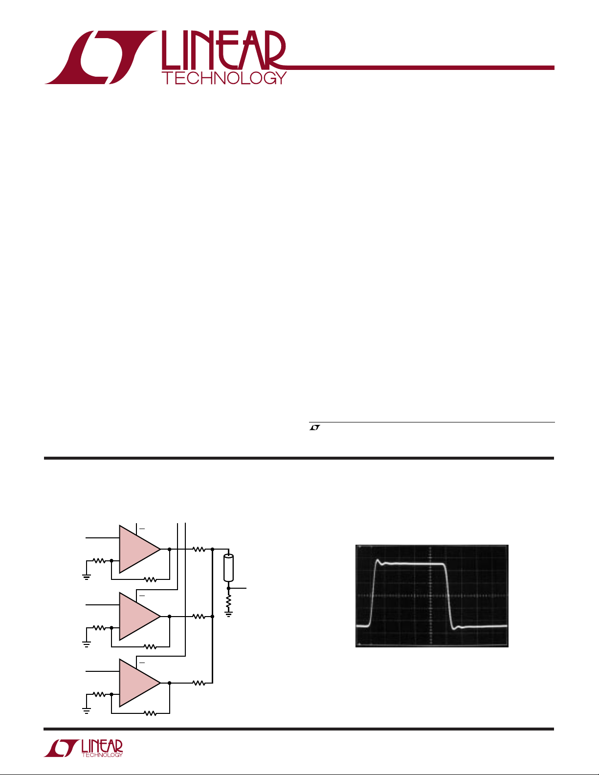
3-Input Video MUX Cable Driver
CHANNEL
A
V
IN A
R
G
200Ω
V
IN B
R
G
200Ω
V
IN C
R
G
200Ω
EN A
+
1/3 LT1399
–
EN B
+
1/3 LT1399
–
EN C
+
1/3 LT1399
–
324Ω
324Ω
324Ω
SELECT
R
F
R
F
R
F
BC
97.6Ω
97.6Ω
97.6Ω
U
1399 TA01
75Ω
75Ω
CABLE
The LT1398/LT1399/LT1399HV are manufactured on Linear Technology’s proprietary complementary bipolar process. The LT1399/LT1399HV are pin-for-pin upgrades to
the LT1260 optimized for use on ±5V/±7.5V supplies.
, LTC and LT are registered trademarks of Linear Technology Corporation.
Square Wave Response
V
OUT
OUTPUT
200mV/DIV
RL = 100Ω
= RG = 324Ω
R
F
f = 10MHz
TIME (10ns/DIV)
1398/99 TA02
1
Page 2
LT1398/LT1399/LT1399HV
W
O
A
LUTEXI TIS
S
Total Supply Voltage (V+ to V–)
LT1398/LT1399 ................................................ 12.6V
LT1399HV ....................................................... 15.5V
Input Current (Note 2) ....................................... ±10mA
Output Current................................................. ±100mA
Differential Input Voltage (Note 2) ........................... ±5V
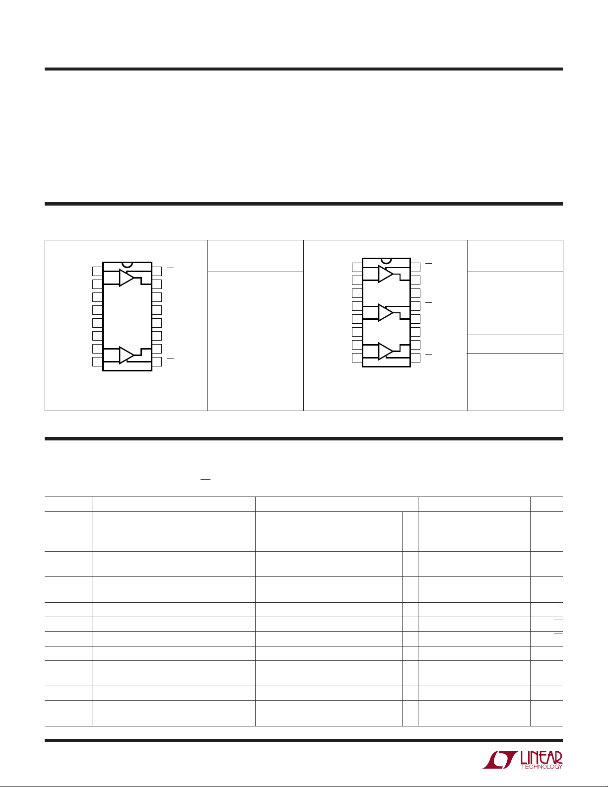
PACKAGE
1
–IN A
2
+IN A
3
*GND
4
*GND
5
*GND
6
*GND
7
+IN B
8
–IN B
16-LEAD PLASTIC SO
T
= 150°C, θJA = 100°C/W
JMAX
*Ground pins are not internally connected. For best channel isolation, connect to ground. Consult factory for Industrial and Military grade parts.
A
/
O
RDER I FOR ATIO
TOP VIEW
A
B
S PACKAGE
16
15
14
13
12
11
10
9
WUW
EN A
OUT A
+
V
GND*
GND*
–
V
OUT B
EN B
U
ARB
G
WU
ORDER PART
NUMBER
LT1398CS
(Note 1)
Output Short-Circuit Duration (Note 3)........ Continuous
Operating Temperature Range ............... – 40°C to 85°C
Specified Temperature Range (Note 4).. –40°C to 85°C
Storage Temperature Range ................ –65°C to 150°C
Junction Temperature (Note 5)............................ 150°C
Lead Temperature (Soldering, 10 sec)................. 300°C
U
TOP VIEW
1
–IN R
2
+IN R
3
*GND
4
–IN G
5
+IN G
6
*GND
7
+IN B
8
–IN B
GN PACKAGE
16-LEAD PLASTIC SSOP
T
= 150°C, θJA = 120°C/W (GN)
JMAX
= 150°C, θJA = 100°C/W (S)
T
JMAX
R
G
B
16
15
14
13
12
11
10
9
S PACKAGE
16-LEAD PLASTIC SO
EN R
OUT R
+
V
EN G
OUT G
–
V
OUT B
EN B
ORDER PART
NUMBER
LT1399CGN
LT1399CS
LT1399HVCS
GN PART MARKING
1399
LECTRICAL C CHARA TERIST
E
(LT1398/LT1399)
ICS
The ● denotes specifications which apply over the specified operating temperature range, otherwise specifications are at TA = 25°C.
For each amplifier: VCM = 0V, V
SYMBOL PARAMETER CONDITIONS MIN TYP MAX UNITS
V
OS
∆VOS/∆T Input Offset Voltage Drift ● 15 µV/°C
+
I
IN
–
I
IN
e
n
+i
n
–i
n
R
IN
C
IN
C
OUT
V
INH
Input Offset Voltage 1.5 10 mV
Noninverting Input Current 10 25 µA
Inverting Input Current 10 50 µA
Input Noise Voltage Density f = 1kHz, RF = 1k, RG = 10Ω, RS = 0Ω 4.5 nV/√Hz
Noninverting Input Noise Current Density f = 1kHz 6 pA/√Hz
Inverting Input Noise Current Density f = 1kHz 25 pA/√Hz
Input Resistance VIN = ±3.5V ● 0.3 1 MΩ
Input Capacitance Amplifier Enabled 2.0 pF
Output Capacitance Amplifier Disabled 8.5 pF
Input Voltage Range, High VS = ±5V ● 3.5 4.0 V
= ±5V, EN = 0V, pulse tested, unless otherwise noted. (Note 4)
S
● 12 mV
● 30 µA
● 60 µA
Amplifier Disabled 2.5 pF
V
= 5V, 0V 4.0 V
S
2
Page 3
LT1398/LT1399/LT1399HV
LECTRICAL C CHARA TERIST
E
(LT1398/LT1399)
ICS
The ● denotes specifications which apply over the specified operating temperature range, otherwise specifications are at TA = 25°C.
For each amplifier: VCM = 0V, V
SYMBOL PARAMETER CONDITIONS MIN TYP MAX UNITS
V
INL
V
OUTH
V
OUTL
V
OUTH
V
OUTL
CMRR Common Mode Rejection Ratio VCM = ±3.5V ● 42 52 dB
–I
CMRR
PSRR Power Supply Rejection Ratio VS = ±2V to ±5V, EN = V
+I
PSRR
–I
PSRR
A
V
R
OL
I
OUT
I
S
I
EN
SR Slew Rate (Note 6) AV = 10, RL = 150Ω 500 800 V/µs
t
ON
t
OFF
tr, t
f
t
PD
os Small-Signal Overshoot RF = RG = 324Ω, RL = 100Ω, V
t
S
dG Differential Gain (Note 8) RF = RG = 324Ω, RL = 150Ω 0.13 %
dP Differential Phase (Note 8) RF = RG = 324Ω, RL = 150Ω 0.10 DEG
Input Voltage Range, Low VS = ±5V ● –3.5 –4.0 V
Maximum Output Voltage Swing, High VS = ±5V, RL = 100k 3.9 4.2 V
Maximum Output Voltage Swing, Low VS = ±5V, RL = 100k –3.9 – 4.2 V
Maximum Output Voltage Swing, High VS = ±5V, RL = 150Ω 3.4 3.6 V
Maximum Output Voltage Swing, Low VS = ±5V, RL = 150Ω –3.4 –3.6 V
Inverting Input Current VCM = ±3.5V 10 16 µA/V
Common Mode Rejection V
Noninverting Input Current VS = ±2V to ±5V, EN = V
Power Supply Rejection
Inverting Input Current VS = ±2V to ±5V, EN = V
Power Supply Rejection
Large-Signal Voltage Gain V
Transimpedance, ∆V
Maximum Output Current RL = 0Ω ● 80 mA
Supply Current per Amplifier V
Disable Supply Current per Amplifier EN Pin Voltage = 4.5V, RL = 150Ω ● 0.1 100 µA
Enable Pin Current 30 110 µA
Turn-On Delay Time (Note 7) RF = RG = 324Ω, RL = 100Ω 30 75 ns
Turn-Off Delay Time (Note 7) RF = RG = 324Ω, RL = 100Ω 40 100 ns
Small-Signal Rise and Fall Time RF = RG = 324Ω, RL = 100Ω, V
Propagation Delay RF = RG = 324Ω, RL = 100Ω, V
Settling Time 0.1%, AV = –1, RF = RG = 309Ω, RL = 150Ω 25 ns
= ±5V, EN = 0V, pulse tested, unless otherwise noted. (Note 4)
S
VS = 5V, 0V 1.0 V
V
= ±5V, RL = 100k ● 3.7 V
S
VS = 5V, 0V; RL = 100k 4.2 V
VS = ±5V, RL = 100k ● –3.7 V
V
= 5V, 0V; RL = 100k 0.8 V
S
VS = ±5V, RL = 150Ω ● 3.2 V
V
= 5V, 0V; RL = 150Ω 3.6 V
S
VS = ±5V, RL = 150Ω ● –3.2 V
V
= 5V, 0V; RL = 150Ω 0.6 V
S
= ±3.5V ● 22 µA/V
OUT
/∆I
CM
= ±2V, RL = 150Ω 50 65 dB
–
IN
OUT
V
= ±2V, RL = 150Ω 40 100 kΩ
OUT
= 0V ● 4.6 6.5 mA
OUT
–
–
–
= 1V
OUT
P-P
= 1V
OUT
P-P
= 1V
OUT
P-P
● 56 70 dB
12 µA/V
● 3 µA/V
● 27 µA/V
● 200 µA
1.3 ns
2.5 ns
10 %
3
Page 4

LT1398/LT1399/LT1399HV
LECTRICAL C CHARA TERIST
E
ICS
(LT1399HV)
The ● denotes specifications which apply over the specified operating temperature range, otherwise specifications are at TA = 25°C.
For each amplifier: VCM = 0V, V
SYMBOL PARAMETER CONDITIONS MIN TYP MAX UNITS
V
OS
∆VOS/∆T Input Offset Voltage Drift ● 15 µV/°C
+
I
IN
–
I
IN
e
n
+i
n
–i
n
R
IN
C
IN
C
OUT
V
INH
V
INL
V
OUTH
V
OUTL
V
OUTH
V
OUTL
CMRR Common Mode Rejection Ratio VCM = ±6V ● 42 52 dB
–I
CMRR
PSRR Power Supply Rejection Ratio VS = ±2V to ±7.5V, EN = V
+I
PSRR
–I
PSRR
A
V
R
OL
I
OUT
I
S
I
EN
Input Offset Voltage 1.5 10 mV
Noninverting Input Current 10 25 µA
Inverting Input Current 10 50 µA
Input Noise Voltage Density f = 1kHz, RF = 1k, RG = 10Ω, RS = 0Ω, VS = ±5V 4.5 nV/√Hz
Noninverting Input Noise Current Density f = 1kHz, VS = ±5V 6 pA/√Hz
Inverting Input Noise Current Density f = 1kHz, VS = ±5V 25 pA/√Hz
Input Resistance VIN = ±6V ● 0.3 1 MΩ
Input Capacitance Amplifier Enabled 2.0 pF
Output Capacitance Amplifier Disabled 8.5 pF
Input Voltage Range, High VS = ±7.5V ● 6 6.5 V
Input Voltage Range, Low VS = ±7.5V ● –6 –6.5 V
Maximum Output Voltage Swing, High VS = ±7.5V, RL = 100k 6.4 6.7 V
Maximum Output Voltage Swing, Low VS = ±7.5V, RL = 100k –6.4 –6.7 V
Maximum Output Voltage Swing, High VS = ±7.5V, RL = 150Ω 5.4 5.8 V
Maximum Output Voltage Swing, Low VS = ±7.5V, RL = 150Ω – 5.4 –5.8 V
Inverting Input Current VCM = ±6V 10 16 µA/V
Common Mode Rejection V
Noninverting Input Current VS = ±2V to ±7.5V, EN = V
Power Supply Rejection
Inverting Input Current VS = ±2V to ±7.5V, EN = V
Power Supply Rejection
Large-Signal Voltage Gain V
Transimpedance, ∆V
Maximum Output Current RL = 0Ω ● 80 mA
Supply Current per Amplifier V
Disable Supply Current per Amplifier EN Pin Voltage = 7V, RL = 150Ω ● 0.1 100 µA
Enable Pin Current 30 110 µA
= ±7.5V, EN = 0V, pulse tested, unless otherwise noted. (Note 4)
S
Amplifier Disabled 2.5 pF
= 7.5V, 0V 6.5 V
V
S
VS = 7.5V, 0V 1.0 V
V
= ±7.5V, RL = 100k ● 6.1 V
S
VS = 7.5V, 0V; RL = 100k 6.7 V
VS = ±7.5V, RL = 100k ● –6.1 V
V
= 7.5V, 0V; RL = 100k 0.8 V
S
VS = ±7.5V, RL = 150Ω ● 5.1 V
V
= 7.5V, 0V; RL = 150Ω 5.8 V
S
VS = ±7.5V, RL = 150Ω ● – 5.1 V
V
= 7.5V, 0V; RL = 150Ω 0.6 V
S
= ±6V ● 22 µA/V
OUT
/∆I
CM
= ±4.5V, RL = 150Ω 50 65 dB
–
IN
OUT
V
= ±4.5V, RL = 150Ω 40 100 kΩ
OUT
= 0V ● 4.6 7 mA
OUT
–
–
–
● 12 mV
● 30 µA
● 60 µA
● 56 70 dB
12 µA/V
● 3 µA/V
● 27 µA/V
● 200 µA
4
Page 5
LT1398/LT1399/LT1399HV
LECTRICAL C CHARA TERIST
E
ICS
(LT1399HV)
The ● denotes specifications which apply over the specified operating temperature range, otherwise specifications are at TA = 25°C.
For each amplifier: VCM = 0V, V
SYMBOL PARAMETER CONDITIONS MIN TYP MAX UNITS
SR Slew Rate (Note 6) AV = 10, RL = 150Ω, VS = ±5V 500 800 V/µs
t
ON
t
OFF
tr, t
f
t
PD
os Small-Signal Overshoot RF = RG = 324Ω, RL = 100Ω, V
t
S
dG Differential Gain (Note 8) RF = RG = 324Ω, RL = 150Ω, VS = ±5V 0.13 %
dP Differential Phase (Note 8) RF = RG = 324Ω, RL = 150Ω, VS = ±5V 0.10 DEG
Note 1: Absolute Maximum Ratings are those values beyond which the life
of a device may be impaired.
Note 2: This parameter is guaranteed to meet specified performance
through design and characterization. It has not been tested.
Note 3: A heat sink may be required depending on the power supply
voltage and how many amplifiers have their outputs short circuited.
Note 4: The LT1398/LT1399/LT1399HV are guaranteed to meet specified
performance from 0°C to 70°C and are designed, characterized and
expected to meet these extended temperature limits, but are not tested at
–40°C and 85°C. Guaranteed I grade parts are available, consult factory.
Note 5: TJ is calculated from the ambient temperature TA and the
power dissipation P
LT1398CS, LT1399CS, LT1399HVCS: T
LT1399CGN: T
Turn-On Delay Time (Note 7) RF = RG = 324Ω, RL = 100Ω, VS = ±5V 30 75 ns
Turn-Off Delay Time (Note 7) RF = RG = 324Ω, RL = 100Ω, VS = ±5V 40 100 ns
Small-Signal Rise and Fall Time RF = RG = 324Ω, RL = 100Ω, V
Propagation Delay RF = RG = 324Ω, RL = 100Ω, V
Settling Time 0.1%, AV = –1V, RF = RG = 309Ω, RL = 150Ω,25ns
according to the following formula:
D
= TA + (PD • 120°C/W)
J
= ±7.5V, EN = 0V, pulse tested, unless otherwise noted. (Note 4)
S
= 1V
, 1.3 ns
P-P
= 1V
, 2.5 ns
P-P
= 1V
,10%
P-P
= 0.5V. This specification is guaranteed by design
IN
V
= ±5V
S
VS = ±5V
V
= ±5V
S
V
= ±5V
S
= TA + (PD • 100°C/W)
J
OUT
OUT
OUT
Note 6: Slew rate is measured at ±2V on a ±3V output signal.
Note 7: Turn-on delay time (tON) is measured from control input to
appearance of 1V at the output, for V
time (t
the output for V
and characterization.
Note 8: Differential gain and phase are measured using a Tektronix
TSG120YC/NTSC signal generator and a Tektronix 1780R Video
Measurement Set. The resolution of this equipment is 0.1% and 0.1°.
Ten identical amplifier stages were cascaded giving an effective
resolution of 0.01% and 0.01°.
) is measured from control input to appearance of 0.5V on
OFF
= 1V. Likewise, turn-off delay
IN
U
W
TYPICAL AC PERFOR A CE
SMALL SIGNAL SMALL SIGNAL SMALL SIGNAL
(V) A
V
S
±5 1 100 365 – 300 150 0.05
±5 2 100 324 324 300 150 0
±5 –1 100 309 309 300 150 0
V
R
(Ω)R
L
F
(Ω)R
(Ω) – 3dB BW (MHz) 0.1dB BW (MHz) PEAKING (dB)
G
5
Page 6

LT1398/LT1399/LT1399HV
UW
LPER
R
F
O
ATYPICA
CCHARA TERIST
E
C
ICS
Closed-Loop Gain vs Frequency
(AV = 1)
4
2
0
GAIN (dB)
–2
–4
1M 10M 1G100M
= ±5V
V
S
V
= –10dBm
IN
= 365Ω
R
F
= 100Ω
R
L
FREQUENCY (Hz)
Large-Signal Transient Response
(AV = 1)
1398/99 G01
Closed-Loop Gain vs Frequency
(AV = 2)
10
8
6
GAIN (dB)
4
2
1M 10M 1G100M
VS = ±5V
V
= –10dBm
IN
= RG = 324Ω
R
F
= 100Ω
R
L
FREQUENCY (Hz)
Large-Signal Transient Response
(AV = 2)
1398/99 G02
Closed-Loop Gain vs Frequency
(AV = – 1)
4
2
0
GAIN (dB)
–2
–4
1M 10M 1G100M
VS = ±5V
= –10dBm
V
IN
= RG = 309Ω
R
F
R
= 100Ω
L
FREQUENCY (Hz)
Large-Signal Transient Response
(AV = – 1)
1398/99 G03
OUTPUT (1V/DIV)
V
IN
R
= 365Ω
F
= 100Ω
R
L
= ±2.5V
TIME (5ns/DIV)VS = ±5V
2nd and 3rd Harmonic Distortion
vs Frequency
30
TA = 25°C
R
= RG = 324Ω
F
40
= 100Ω
R
L
= ±5V
V
S
50
= 2VPP
V
OUT
60
70
80
DISTORTION (dB)
90
100
110
10
1 100 1000 100000
FREQUENCY (kHz)
HD2
HD3
10000
1398/99 G04
1398/1399 G07
OUTPUT (1V/DIV)
V
= ±1.25V
IN
= RG = 324Ω
R
F
= 100Ω
R
L
TIME (5ns/DIV)VS = ±5V
Maximum Undistorted Output
Voltage vs Frequency
8
7
)
P-P
6
5
4
OUTPUT VOLTAGE (V
TA = 25°C
= 324Ω
R
F
3
= 100Ω
R
L
= ±5V
V
S
2
1
FREQUENCY (MHz)
AV = +1 AV = +2
10 100
1398/99 G05
1398/1399 G08
OUTPUT (1V/DIV)
V
= ±2.5V
IN
= RG = 309Ω
R
F
= 100Ω
R
L
TIME (5ns/DIV)VS = ±5V
PSRR vs Frequency
80
70
60
= RG = 324Ω
F
= 100Ω
L
= +2
V
100k
–PSRR
50
40
PSRR (dB)
30
20
TA = 25°C
R
10
R
A
0
10k 1M 10M 100M
+PSRR
FREQUENCY (Hz)
1398/99 G06
1398/1399 G09
6
Page 7

LPER
SUPPLY VOLTAGE (±V)
0
0
SUPPLY CURRENT (mA)
1
3
4
5
2
4
59
1398/1399 G15
2
13
6
7
8
6
EN = V
–
EN = 0V
AMBIENT TEMPERATURE (°C)
–50
POSITIVE SUPPLY CURRENT PER AMPLIFIER (mA)
4.75
25
1398/1399 G18
4.00
3.50
–25 0 50
3.25
3.00
5.00
4.50
4.25
3.75
75 100 125
EN = –5V
EN = 0
VS = ±5V
F
O
R
ATYPICA
UW
CCHARA TERIST
E
C
LT1398/LT1399/LT1399HV
ICS
Input Voltage Noise and Current
Noise vs Frequency
1000
100
–IN
+IN
EN
FREQUENCY (Hz)
INPUT NOISE (nV/√Hz OR pA/√Hz)
10
1
10
30 100 300 1k 3k 10k 30k 100k
Maximum Capacitive Load
vs Feedback Resistor
1000
100
1398/1399 G10
Output Impedance vs Frequency
100
RF = RG = 324Ω
= 50Ω
R
L
= +2
A
V
= ±5V
V
S
10
1
0.1
OUTPUT IMPEDANCE (Ω)
0.01
10k
1M 10M100k 100M
FREQUENCY (Hz)
Capacitive Load
vs Output Series Resistor
40
30
RF = RG = 324Ω
= ±5V
V
S
OVERSHOOT < 2%
1398/1399 G11
Output Impedance (Disabled)
vs Frequency
100k
10k
1k
OUTPUT IMPEDANCE (DISABLED) (Ω)
100
100k
1M 10M 100M
FREQUENCY (Hz)
Supply Current vs Supply Voltage
RF = 365Ω
= +1
A
V
= ±5V
V
S
1398/1399 G12
10
CAPACITIVE LOAD (pF)
1
300
5
4
3
2
1
0
–1
–2
–3
OUTPUT VOLTAGE SWING (V)
–4
–5
–50
RF = R
AV = +2
V
PEAKING ≤ 5dB
900 1500 2100 2700 3300
FEEDBACK RESISTANCE (Ω)
Output Voltage Swing
vs Temperature
RL = 150ΩRL = 100k
0
–25
AMBIENT TEMPERATURE (°C)
RL = 150ΩRL = 100k
50
25
= ±5V
S
75
G
1398/1399 G13
100
1398/1399 G16
125
20
10
OUTPUT SERIES RESISTANCE (Ω)
0
10
Enable Pin Current
vs Temperature
–10
VS = ±5V
–20
–30
–40
–50
–60
ENABLE PIN CURRENT (µA)
–70
–80
–50
–25 0
AMBIENT TEMPERATURE (°C)
100 1000
CAPACITIVE LOAD (pF)
EN = 0V
EN = –5V
50 100 125
25 75
1398/1399 G14
Positive Supply Current per
Amplifier vs Temperature
1398/1399 G17
7
Page 8

LT1398/LT1399/LT1399HV
UW
LPER
F
O
R
ATYPICA
CCHARA TERIST
E
C
ICS
Input Offset Voltage
vs Temperature
3.0
VS = ±5V
2.5
2.0
1.5
1.0
0.5
0
INPUT OFFSET VOLTAGE (mV)
–0.5
–1.0
–25 0 50
–50
25
AMBIENT TEMPERATURE (°C)
75 100 125
All Hostile Crosstalk
0
RF = RG = 324Ω
–10
= 100Ω
R
L
= +2
A
V
–20
–30
–40
–50
–60
–70
–80
ALL HOSTILE CROSSTALK (dB)
–90
–100
R
G
B
100k 10M 100M 500M
1M
FREQUENCY (Hz)
1398/1399 G19
1398/1399 G21
Input Bias Currents
vs Temperature
15
VS = ±5V
12
9
6
3
0
INPUT BIAS CURRENT (µA)
–3
–6
–50
–25 0
+
I
B
–
I
B
50 100 125
25 75
AMBIENT TEMPERATURE (°C)
All Hostile Crosstalk (Disabled)
–10
RF = RG = 324Ω
–20
= 100Ω
R
L
= +2
A
V
–30
–40
–50
–60
–70
–80
–90
ALL HOSTILE CROSSTALK (dB)
–100
–110
R
G
B
100k 10M 100M 500M
1M
FREQUENCY (Hz)
1398/99 G20
1398/1399 G24
8
INPUT
100mV/DIV
Propagation Delay
tPD = 2.5ns
= 100Ω
R
L
= RG = 324Ω
R
F
TIME (500ps/DIV)AV = +2
Rise Time and Overshoot
V
OUT
OUTPUT
200mV/DIV
1398/1399 G22 1398/1399 G23
200mV/DIV
= +2
V
= 100Ω
R
L
= RG = 324Ω
R
F
tr = 1.3ns
TIME (500ps/DIV)A
OS = 10%
Page 9

UUU
PIN FUNCTIONS
LT1398/LT1399/LT1399HV
LT1398
– IN A (Pin 1): Inverting Input of A Channel Amplifier.
+ IN A (Pin 2): Noninverting Input of A Channel Amplifier.
GND (Pins 3, 4, 5, 6): Ground. Not connected internally.
+ IN B (Pin 7): Noninverting Input of B Channel Amplifier.
– IN B (Pin 8): Inverting Input of B Channel Amplifier.
EN B (Pin 9): B Channel Enable Pin. Logic low to enable.
OUT B (Pin 10): B Channel Output.
V– (Pin 11): Negative Supply Voltage, Usually –5V.
GND (Pins 12, 13): Ground. Not connected internally.
V+ (Pin 14): Positive Supply Voltage, Usually 5V.
OUT A (Pin 15): A Channel Output.
EN A (Pin 16): A Channel Enable Pin. Logic low to enable.
LT1399, LT1399HV
– IN R (Pin 1): Inverting Input of R Channel Amplifier.
+ IN R (Pin 2): Noninverting Input of R Channel Amplifier.
GND (Pin 3): Ground. Not connected internally.
– IN G (Pin 4): Inverting Input of G Channel Amplifier.
+ IN G (Pin 5): Noninverting Input of G Channel Amplifier.
GND (Pin 6): Ground. Not connected internally.
+ IN B (Pin 7): Noninverting Input of B Channel Amplifier.
– IN B (Pin 8): Inverting Input of B Channel Amplifier.
EN B (Pin 9): B Channel Enable Pin. Logic low to enable.
OUT B (Pin 10): B Channel Output.
V– (Pin 11): Negative Supply Voltage, Usually –5V.
OUT G (Pin 12): G Channel Output.
EN G (Pin 13): G Channel Enable Pin. Logic low to enable.
V+ (Pin 14): Positive Supply Voltage, Usually 5V.
U
O
PPLICATI
A
Feedback Resistor Selection
The small-signal bandwidth of the LT1398/LT1399/
LT1399HV is set by the external feedback resistors and the
internal junction capacitors. As a result, the bandwidth is
a function of the supply voltage, the value of the feedback
resistor, the closed-loop gain and the load resistor. The
LT1398/LT1399 have been optimized for ±5V supply
operation and have a – 3dB bandwidth of 300MHz at a gain
of 2. The LT1399HV provides performance similar to the
LT1399. Please refer to the resistor selection guide in the
Typical AC Performance table.
Capacitance on the Inverting Input
Current feedback amplifiers require resistive feedback
from the output to the inverting input for stable operation.
S
I FOR ATIO
WU
U
OUT R (Pin 15): R Channel Output.
EN R (Pin 16): R Channel Enable Pin. Logic low to enable.
Take care to minimize the stray capacitance between the
output and the inverting input. Capacitance on the inverting input to ground will cause peaking in the frequency
response (and overshoot in the transient response).
Capacitive Loads
The LT1398/LT1399/LT1399HV can drive many capacitive loads directly when the proper value of feedback
resistor is used. The required value for the feedback
resistor will increase as load capacitance increases and as
closed-loop gain decreases. Alternatively, a small resistor
(5Ω to 35Ω) can be put in series with the output to isolate
the capacitive load from the amplifier output. This has the
advantage that the amplifier bandwidth is only reduced
when the capacitive load is present. The disadvantage is
that the gain is a function of the load resistance.
9
Page 10

LT1398/LT1399/LT1399HV
PPLICATI
A
U
O
S
I FOR ATIO
WU
U
Power Supplies
The LT1398/LT1399 will operate from single or split
supplies from ±2V (4V total) to ±6V (12V total). The
LT1399HV will operate from single or split supplies from
±2V (4V total) to ±7.5V (15V total). It is not necessary to
use equal value split supplies, however the offset voltage
and inverting input bias current will change. The offset
voltage changes about 600µV per volt of supply mis-
match. The inverting bias current will typically change
about 2µA per volt of supply mismatch.
Slew Rate
Unlike a traditional voltage feedback op amp, the slew rate
of a current feedback amplifier is not independent of the
amplifier gain configuration. In a current feedback amplifier, both the input stage and the output stage have slew rate
limitations. In the inverting mode, and for gains of 2 or more
in the noninverting mode, the signal amplitude between the
input pins is small and the overall slew rate is that of the
output stage. For gains less than 2 in the noninverting mode,
the overall slew rate is limited by the input stage.
The input slew rate of the LT1398/LT1399/LT1399HV is
approximately 600V/µs and is set by internal currents and
capacitances. The output slew rate is set by the value of the
feedback resistor and internal capacitance. At a gain of 2
with 324Ω feedback and gain resistors and ±5V supplies,
the output slew rate is typically 800V/µs. Larger feedback
resistors will reduce the slew rate as will lower supply
voltages.
Enable/ Disable
will remain enabled at all times, then the EN pin should be
tied to the V– supply. The enable pin current is approximately 30µA when activated. If using CMOS open-drain
logic, an external 1k pull-up resistor is recommended to
ensure that the LT1399 remains disabled in spite of any
CMOS drain-leakage currents.
5.0
TA = 25°C
+
4.5
V
= 5V
= 100Ω
R
L
–
= 0V
V
4
5
6
1398/99 F01
7
OUTPUT
EN
1398/99 F02
4.0
3.5
3.0
2.5
(mA)
S
+I
2.0
1.5
1.0
0.5
0
0
V– = –5V
3
2
1
V+ – VEN (V)
Figure 1. +IS vs (V+ – VEN)
VS = ±5V
V
= 1V
IN
= 324Ω
R
F
R
= 324Ω
G
Figure 2. Amplifier Enable Time, AV = 2
Each amplifier of the LT1398/LT1399/LT1399HV has a
unique high impedance, zero supply current mode which
is controlled by its own EN pin. These amplifiers are
designed to operate with CMOS logic; the amplifiers draw
zero current when these pins are high. To activate each
amplifier, its EN pin is normally pulled to a logic low.
However, supply current will vary as the voltage between
the V+ supply and EN is varied. As seen in Figure 1, +I
S
does vary with (V+ – VEN), particularly when the voltage
difference is less than 3V. For normal operation, it is
important to keep the EN pin at least 3V below the V
+
supply. If a V+ of less than 3V is desired, and the amplifier
10
VS = ±5V
= 1V
V
IN
R
= 324Ω
F
= 324Ω
R
G
R
= 100Ω
L
1398/99 F03
Figure 3. Amplifier Disable Time, AV = 2
OUTPUT
EN
Page 11

LT1398/LT1399/LT1399HV
PPLICATI
A
U
O
S
I FOR ATIO
WU
U
The enable/disable times are very fast when driven from
standard 5V CMOS logic. Each amplifier enables in about
30ns (50% point to 50% point) while operating on ±5V
supplies (Figure 2). Likewise, the disable time is approximately 40ns (50% point to 50% point) (Figure 3).
Differential Input Signal Swing
To avoid any breakdown condition on the input transistors, the differential input swing must be limited to ±5V. In
normal operation, the differential voltage between the
input pins is small, so the ±5V limit is not an issue. In the
disabled mode however, the differential swing can be the
same as the input swing, and there is a risk of device
breakdown if input voltage range has not been properly
considered.
3-Input Video MUX Cable Driver
The application on the first page of this data sheet shows
a low cost, 3-input video MUX cable driver. The scope
photo below (Figure 4) displays the cable output of a
30MHz square wave driving 150Ω. In this circuit the
active amplifier is loaded by the sum of RF and RG of each
disabled amplifier. Resistor values have been chosen to
keep the total back termination at 75Ω while maintaining
a gain of 1 at the 75Ω load. The switching time between
any two channels is approximately 32ns when both
enable pins are driven.
EN A
EN B
OUTPUT
VS = ±5V 20ns/DIV
V
= V
= 2V
INA
INB
at 3.58MHz
Figure 5. 3-Input Video MUX Switching Response (AV = 2)
P-P
1398/99 F05
Using the LT1399 to Drive LCD Displays
Driving the current crop of XGA and UXGA LCD displays
can be a difficult problem because they require drive
voltages of up to 12V, are usually a capacitive load of over
300pF, and require fast settling. The LT1399HV is particularly well suited for driving these LCD displays because it is capable of swinging more than ±6V on ±7.5V
supplies, and it can drive large capacitive loads with a
small series resistor at the output, minimizing settling
time. As seen in Figures 6 and 7, at a gain of +3 with a
16.9Ω output series resistor and a 330pF load, the
LT1399HV is capable of settling to 0.1% in 30ns for a 6V
step. Similarly, a 12V output step settles in 70ns.
When building the board, care was taken to minimize
trace lengths at the inverting input. The ground plane was
also pulled away from RF and RG on both sides of the
board to minimize stray capacitance.
OUTPUT
200mV/DIV
RL = 150Ω
= RG = 324Ω
R
F
f = 10MHz
Figure 4. Square Wave Response
5ns/DIV
1398/99 F04
V
IN
V
OUT
VS = ±5V 20ns/DIV
= 324Ω
R
F
R
= 162Ω
G
= 16.9Ω
R
S
= 330pF
C
L
Figure 6. LT1399/LT1399HV Large-Signal Pulse Response
1398/99 AI06
11
Page 12

LT1398/LT1399/LT1399HV
PPLICATI
A
V
IN
V
OUT
U
O
S
I FOR ATIO
VS = ±7.5V 50ns/DIV
= 324Ω
R
F
= 162Ω
R
G
R
= 16.9Ω
S
= 330pF
C
L
WU
1398/99 F07
U
Figure 7. LT1399HV Output Voltage Swing
Buffered RGB to Color-Difference Matrix
Two LT1398s can be used to create buffered colordifference signals from RGB inputs (Figure 8). In this
application, the R input arrives via 75Ω coax. It is routed
to the noninverting input of LT1398 amplifier A1 and to
a 1082Ω resistor R8. There is also an 80.6Ω termination
resistor R11, which yields a 75Ω input impedance at the
R input when considered in parallel with R8. R8 connects
to the inverting input of a second LT1398 amplifier (A2),
which also sums the weighted G and B inputs to create a
–0.5 • Y output. LT1398 amplifier B1 then takes the
–0.5 • Y output and amplifies it by a gain of –2, resulting
in the Y output. Amplifier A1 is configured in a noninverting gain of 2 with the bottom of the gain resistor R2 tied
to the Y output. The output of amplifier A1 thus results in
the color-difference output R-Y.
The B input is similar to the R input. It arrives via 75Ω
coax, and is routed to the noninverting input of LT1398
amplifier B2, and to a 2940Ω resistor R10. There is also
a 76.8Ω termination resistor R13, which yields a 75Ω
input impedance when considered in parallel with R10.
R10 also connects to the inverting input of amplifier A2,
adding the B contribution to the Y signal as discussed
above. Amplifier B2 is configured in a noninverting gain
of 2 configuration with the bottom of the gain resistor R4
tied to the Y output. The output of amplifier B2 thus
results in the color-difference output B-Y.
75Ω
SOURCES
R
G
B
+
1/2 LT1398
–
–
1/2 LT1398
+
R11
80.6Ω
R12
86.6Ω
R13
76.8Ω
R8
1082Ω
R9
549Ω
R10
2940Ω
R7
324Ω
–
A2
1/2 LT1398
+
R6
162Ω
–
ALL RESISTORS 1%
= ±5V
V
S
1/2 LT1398
+
Figure 8. Buffered RGB to Color-Difference Matrix
A1
B1
B2
R5
324Ω
R1
324Ω
R2
324Ω
R4
324Ω
R3
324Ω
1398/99 F08
R-Y
Y
B-Y
12
Page 13

LT1398/LT1399/LT1399HV
PPLICATI
A
U
O
S
I FOR ATIO
WU
U
The G input also arrives via 75Ω coax and adds its
contribution to the Y signal via a 549Ω resistor R9, which
is tied to the inverting input of amplifier A2. There is also
an 86.6Ω termination resistor R12, which yields a 75Ω
termination when considered in parallel with R9. Using
superposition, it is straightforward to determine the
output of amplifier A2. Although inverted, it sums the R,
G and B signals in the standard proportions of 0.3R,
0.59G and 0.11B that are used to create the Y signal.
Amplifier B1 then inverts and amplifies the signal by 2,
resulting in the Y output.
Buffered Color-Difference to RGB Matrix
The LT1399 can be used to create buffered RGB outputs
from color-difference signals (Figure 9). The R output is
a back-terminated 75Ω signal created using resistor R5
and LT1399 amplifier A1 configured for a gain of +2 via
324Ω resistors R3 and R4. The noninverting input of
amplifier A1 is connected via 1k resistors R1 and R2 to
the Y and R-Y inputs respectively, resulting in cancellation of the Y signal at the amplifier input. The remaining
R signal is then amplified by A1.
The B output is also a back-terminated 75Ω signal
created using resistor R16 and amplifier A3 configured
for a gain of +2 via 324Ω resistors R14 and R15. The
noninverting input of amplifier A3 is connected via 1k
resistors R12 and R13 to the Y and B-Y inputs respectively, resulting in cancellation of the Y signal at the
amplifier input. The remaining B signal is then amplified
by A3.
The G output is the most complicated of the three. It is a
weighted sum of the Y, R-Y and B-Y inputs. The Y input
is attenuated via resistors R6 and R7 such that amplifier
A2’s noninverting input sees 0.83Y. Using superposition,
we can calculate the positive gain of A2 by assuming that
R8 and R9 are grounded. This results in a gain of 2.41 and
a contribution at the output of A2 of 2Y. The R-Y input is
amplified by A2 with the gain set by resistors R8 and R10,
giving an amplification of –1.02. This results in a contribution at the output of A2 of 1.02Y – 1.02R. The B-Y input
is amplified by A2 with the gain set by resistors R9 and
R10, giving an amplification of –0.37. This results in a
contribution at the output of A2 of 0.37Y – 0.37B.
If we now sum the three contributions at the output of A2,
we get:
A2
= 3.40Y – 1.02R – 0.37B
OUT
It is important to remember though that Y is a weighted
sum of R, G and B such that:
Y = 0.3R + 0.59G + 0.11B
If we substitute for Y at the output of A2 we then get:
A2
= (1.02R – 1.02R) + 2G + (0.37B – 0.37B)
OUT
= 2G
The back-termination resistor R11 then halves the output
of A2 resulting in the G output.
R1
Y
R-Y
B-Y
ALL RESISTORS 1%
= ±5V
V
S
Figure 9. Buffered Color-Difference to RGB Matrix
1k
R2
1k
R6
205Ω
R8
316Ω
R9
845Ω
R12
1k
R13
1k
R3
324Ω
R4
324Ω
R10
324Ω
R14
324Ω
R15
324Ω
1398/99 F09
R5
75Ω
R11
75Ω
R16
75Ω
R
G
B
+
A1
1/3 LT1399
–
+
R7
1k
A2
1/3 LT1399
–
+
A3
1/3 LT1399
–
13
Page 14

LT1398/LT1399/LT1399HV
WW
SI PLIFIED SCHE ATIC
, each amplifier
+
V
+IN
EN
–IN
OUT
–
V
1398/99 SS
14
Page 15

PACKAGE DESCRIPTIO
LT1398/LT1399/LT1399HV
U
Dimensions in inches (millimeters) unless otherwise noted.
GN Package
16-Lead Plastic SSOP (Narrow 0.150)
(LTC DWG # 05-08-1641)
0.189 – 0.196*
(4.801 – 4.978)
16
15
14
12 11 10
13
0.009
(0.229)
9
REF
0.015
± 0.004
(0.38 ± 0.10)
0.007 – 0.0098
(0.178 – 0.249)
0.016 – 0.050
(0.406 – 1.270)
* DIMENSION DOES NOT INCLUDE MOLD FLASH. MOLD FLASH
SHALL NOT EXCEED 0.006" (0.152mm) PER SIDE
** DIMENSION DOES NOT INCLUDE INTERLEAD FLASH. INTERLEAD
FLASH SHALL NOT EXCEED 0.010" (0.254mm) PER SIDE
0° – 8° TYP
× 45°
S Package
16-Lead Plastic Small Outline (Narrow 0.150)
(LTC DWG # 05-08-1610)
0.229 – 0.244
(5.817 – 6.198)
0.053 – 0.068
(1.351 – 1.727)
0.008 – 0.012
(0.203 – 0.305)
16
15
12
0.386 – 0.394*
(9.804 – 10.008)
13
14
0.150 – 0.157**
(3.810 – 3.988)
5
4
3
678
0.004 – 0.0098
(0.102 – 0.249)
0.025
(0.635)
BSC
GN16 (SSOP) 0398
12
11
10
9
0.010 – 0.020
(0.254 – 0.508)
0.008 – 0.010
(0.203 – 0.254)
*
DIMENSION DOES NOT INCLUDE MOLD FLASH. MOLD FLASH
SHALL NOT EXCEED 0.006" (0.152mm) PER SIDE
**
DIMENSION DOES NOT INCLUDE INTERLEAD FLASH. INTERLEAD
FLASH SHALL NOT EXCEED 0.010" (0.254mm) PER SIDE
× 45°
0° – 8° TYP
0.016 – 0.050
0.406 – 1.270
Information furnished by Linear Technology Corporation is believed to be accurate and reliable.
However, no responsibility is assumed for its use. Linear Technology Corporation makes no representation that the interconnection of its circuits as described herein will not infringe on existing patent rights.
0.228 – 0.244
(5.791 – 6.197)
0.053 – 0.069
(1.346 – 1.752)
0.014 – 0.019
(0.355 – 0.483)
0.150 – 0.157**
(3.810 – 3.988)
4
5
0.050
(1.270)
TYP
3
2
1
7
6
8
0.004 – 0.010
(0.101 – 0.254)
S16 0695
15
Page 16

LT1398/LT1399/LT1399HV
U
O
A
PPLICATITYPICAL
Single Supply RGB Video Amplifier
The LT1399 can be used with a single supply voltage of
6V or more to drive ground-referenced RGB video. In
Figure 10, two 1N4148 diodes D1 and D2 have been
placed in series with the output of the LT1399 amplifier
A1 but within the feedback loop formed by resistor R8.
These diodes effectively level-shift A1’s output downward by 2 diodes, allowing the circuit output to swing to
ground.
Amplifier A1 is used in a positive gain configuration. The
feedback resistor R8 is 324Ω. The gain resistor is created
from the parallel combination of R6 and R7, giving a
Thevenin equivalent 80.4Ω connected to 3.75V. This
gives an AC gain of +5 from the noninverting input of
amplifier A1 to the cathode of D2. However, the video
input is also attenuated before arriving at A1’s positive
5V
R1
1000Ω
R2
1300Ω
V
IN
R3
160Ω
R4
75Ω
R5
2.32Ω
R6
107Ω
R7
324Ω
input. Assuming a 75Ω source impedance for the signal
driving VIN, the Thevenin equivalent signal arriving at
A1’s positive input is 3V + 0.4VIN, with a source impedance of 714Ω. The combination of these two inputs gives
an output at the cathode of D2 of 2 • VIN with no additional
DC offset. The 75Ω back termination resistor R9 halves
the signal again such that V
equals a buffered version
OUT
of VIN.
It is important to note that the 4.7µF capacitor C1 has
been added to provide enough current to maintain the
voltage drop across diodes D1 and D2 when the circuit
output drops low enough that the diodes might otherwise
reverse bias. This means that this circuit works fine for
continuous video input, but will require that C1 charge up
after a period of inactivity at the input.
C1
R8
D1
1N4148
4.7µF
D2
1N4148
1398/99 F10
R9
75Ω
V
OUT
V
S
6V TO 12V
+
A1
1/3 LT1399
–
324Ω
Figure 10. Single Supply RGB Video Amplifier (1 of 3 Channels)
RELATED PARTS
PART NUMBER DESCRIPTION COMMENTS
LT1203/LT1205 150MHz Video Multiplexers 2:1 and Dual 2:1 MUXs with 25ns Switch Time
LT1204 4-Input Video MUX with Current Feedback Amplifier Cascadable Enable 64:1 Multiplexing
LT1227 140MHz Current Feedback Amplifier 1100V/µs Slew Rate, Shutdown Mode
LT1252/LT1253/LT1254 Low Cost Video Amplifiers Single, Dual and Quad Current Feedback Amplifiers
LT1259/LT1260 Dual/Triple Current Feedback Amplifier 130MHz Bandwidth, 0.1dB Flatness > 30MHz
LT1675 Triple 2:1 Buffered Video Mulitplexer 2.5ns Switching Time, 250MHz Bandwidth
13989f LT/TP 0699 4K • PRINTED IN USA
LINEAR TECHNOLOGY CORPORATION 1998
16
Linear Technology Corporation
1630 McCarthy Blvd., Milpitas, CA 95035-7417
(408) 432-1900 ● FAX: (408) 434-0507
●
www.linear-tech.com
 Loading...