

Page 1
LT1394
7ns, Low Power,
Single Supply, Ground-Sensing
FEATURES
■
UltraFastTM: 7ns
■
Low Power: 6mA
■
Low Offset Voltage: 0.8mV
■
Operates Off Single 5V or Dual ±5V Supplies
■
Input Common Mode Extends to Negative Supply
■
No Minimum Input Slew Rate Requirement
■
Complementary TTL Outputs
■
Inputs Can Exceed Supplies without Phase Reversal
■
Pin Compatible with LT1016, LT1116 and LT1671
■
Output Latch Capability
■
Available in 8-Lead MSOP and SO Packages
U
APPLICATIO S
■
High Speed A/D Converters
■
Zero-Crossing Detectors
■
Current Sense for Switching Regulators
■
Extended Range V/F Coverters
■
Fast Pulse Height/Width Discriminators
■
High Speed Triggers
■
Line Receivers
■
High Speed Sampling Circuits
, LTC and LT are registered trademarks of Linear Technology Corporation.
UltraFast is a trademark of Linear Technology Corporation.
U
Comparator
DESCRIPTIO
The LT®1394 is an UltraFast (7ns) comparator with complementary outputs and latch. The input common mode range
extends from 1.5V below the positive supply down to the
negative supply rail. Like the LT1016, LT1116 and LT1671,
this comparator has complementary outputs designed to
interface directly to TTL or CMOS logic. The LT1394 may
operate from either a single 5V supply or dual ±5V supplies.
Low offset voltage specifications and high gain allow the
LT1394 to be used in precision applications.
The LT1394 is designed for improved speed and stability for
a wide range of operating conditions. The output stage
provides active drive in both directions for maximum speed
into TTL, CMOS or passive loads with minimal cross-conduction current. Unlike other fast comparators, the LT1394
remains stable even for slow transitions through the active
region, which eliminates the need to specify a minimum input
slew rate.
The LT1394 has an internal, TTL/CMOS compatible latch for
retaining data at the outputs. The latch holds data as long as
the LATCH pin is held high. Device parameters such as gain,
offset and negative power supply current are not significantly
affected by variations in negative supply voltage.
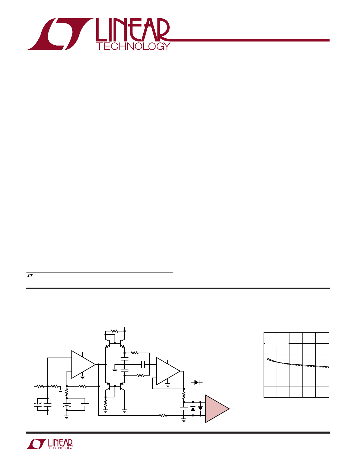
TYPICAL APPLICATIO
45MHz Single Supply Adaptive Trigger
3
Q1 Q2
10µF
5V
+
A1
LT1227
–
750Ω
2k
5V
+
0.1µF
INPUT
510Ω
36Ω
+
100µF
0.1µF
2
13
Q3
15
2k
2k
1
0.005µF
14
U
Propagation Delay vs
5V
6
5
3M
4
500pF
0.005µF
10
12
11
3M
Q4
+
LT1006
–
470Ω
5V
A2
0.1µF
Q1, Q2, Q3, Q4 = CA3096 ARRAY:
TIE SUBSTRATE (PIN 16) TO GROUND
470Ω
= 1N4148
+
LT1394
–
TRIGGER
OUT
1394 F18
12
10
8
6
TIME (ns)
4
2
0
Input Overdrive
TA = 25°C
= 100mV
V
STEP
= ±5V
V
S
0
10 20 30 40
OVERDRIVE (mV)
t
PDLH
t
PDHL
50
1394 TA02
1
Page 2
LT1394
TOP VIEW
Q OUT
Q OUT
GND
V
+
+IN
–IN
V
–
S8 PACKAGE
8-LEAD PLASTIC SO
1
2
3
4
8
7
6
5
+
–
LATCH
ENABLE
WW
W
ABSOLUTE MAXIMUM RATINGS
U
(Note 1)
Total Supply Voltage (V+ to V–) ............................... 12V
Positive Supply Voltage ............................................. 7V
Negative Supply Voltage .......................................... –7V
Differential Input Voltage ....................................... ±12V
Input and Latch Current (Note 2)........................±10mA
Output Current (Continuous)(Note 2) .................±20mA
U
W
PACKAGE/ORDER INFORMATION
TOP VIEW
+
V
1
2
+IN
3
–IN
–
4
V
MS8 PACKAGE
8-LEAD PLASTIC MSOP
T
= 150°C, θJA = 250°C/W
JMAX
8
Q OUT
7
Q OUT
6
GND
5
LATCH
ENABLE
ORDER PART
NUMBER
LT1394CMS8
MS8 PART MARKING
LTBH
Operating Temperature Range ................ –40°C to 85°C
Specified Temperature Range (Note 3)... –40°C to 85°C
Junction Temperature........................................... 150°C
Storage Temperature Range ................. –65°C to 150°C
Lead Temperature (Soldering, 10 sec).................. 300°C
U
ORDER PART
NUMBER
LT1394CS8
LT1394IS8
S8 PART MARKING
T
= 150°C, θJA = 190°C/W
JMAX
1394
1394I
Consult factory for Military grade parts.
ELECTRICAL CHARACTERISTICS
The ● denotes specifications which apply over the full operating temperature range, otherwise specifications are TA = 25°C.
V+ = 5V, V– = –5V, V
SYMBOL PARAMETER CONDITIONS MIN TYP MAX UNITS
V
OS
∆V
OS
∆T
I
OS
I
B
V
CMR
CMRR Common Mode Rejection Ratio –5V ≤ VCM ≤ 3.5V, TA > 0°C 55 100 dB
PSRR Power Supply Rejection Ratio 4.6V ≤ V+ ≤ 5.4V ● 50 65 dB
A
V
V
OH
2
Input Offset Voltage RS ≤ 100Ω (Note 4) 0.8 2.5 mV
Input Offset Voltage Drift ● 4 µV/°C
Input Offset Current 0.1 0.5 µA
Input Bias Current (Note 5) 2 4.5 µA
Input Voltage Range (Note 6) ● –5 3.5 V
Small Signal Voltage Gain 1V ≤ V
Output Voltage Swing High V+ ≥ 4.6V, I
(Q) = 1.4V, V
OUT
= VCM = 0V unless otherwise noted.
LATCH
Single 5V Supply
–5V ≤ V
Single 5V Supply
0V ≤ V
0V ≤ V
–7V ≤ V
+
V
≤ 3.3V, TA ≤ 0°C55 dB
CM
≤ 3.5V, TA > 0°C 55 100 dB
CM
≤ 3.3V, TA ≤ 0°C55 dB
CM
–
≤ –2V ● 65 100 dB
≤ 2V 750 1600 V/V
OUT
≥ 4.6V, I
OUT
OUT
● 4.0 mV
● 0.8 µA
● 7.0 µA
● 0 3.5 V
= 1mA ● 2.7 3.1 V
= 4mA ● 2.4 3.0 V
Page 3
LT1394
ELECTRICAL CHARACTERISTICS
The ● denotes specifications which apply over the full operating temperature range, otherwise specifications are TA = 25°C.
V+ = 5V, V– = –5V, V
SYMBOL PARAMETER CONDITIONS MIN TYP MAX UNITS
V
OL
+
I
–
I
V
IH
V
IL
I
IL
t
PD
∆t
PD
t
LPD
t
SU
t
H
t
PW(D)
Note 1: Absolute Maximum Ratings are those values beyond which the life
of a device may be impaired.
Note 2: This parameter is guaranteed to meet specified perforamnce
through design and characterization. It has not been tested.
Note 3: The LT1394CMS8 and LT1394CS8 are guaranteed to meet
specified performance from 0°C to 70°C and are designed, characterized
and expected to meet these extended temperature limits, but are not tested
at –40°C and 85°C. The LT1394IS8 is guaranteed to meet the extended
temperature limits.
Note 4: Input offset voltage (V
voltages measured by forcing first one output, then the other to 1.4V.
Note 5: Input bias current (I
currents.
Note 6: Input voltage range is guaranteed in part by CMRR testing and in
part by design and characterization.
Output Voltage Swing Low I
Positive Supply Current 6 8.5 mA
Negative Supply Current 1.2 2.2 mA
LATCH Pin High Input Voltage ● 2V
LATCH Pin Low Input Voltage ● 0.8 V
LATCH Pin Current V
Propagation Delay (Note 7) ∆VIN = 100mV, VOD = 5mV 7 9 ns
Differential Propagation Delay (Note 7) ∆VIN = 100mV, VOD = 5mV 0.5 2.2 ns
Latch Propagation Delay (Note 8) 6 ns
Latch Setup Time (Note 8) –0.4 ns
Latch Hold Time (Note 8) 2ns
Minimum Disable Pulse Width 3ns
(Q) = 1.4V, V
OUT
) is defined as the average of the two
OS
) is defined as the average of the two input
B
= VCM = 0V unless otherwise noted.
LATCH
= –4mA ● 0.3 0.5 V
OUT
I
= –10mA 0.4 V
OUT
● 10.0 mA
● 2.5 mA
= 0V ● –4 –10 µA
LATCH
● 14 ns
Note 7: t
and ∆tPD cannot be measured in automatic handling
PD
equipment with low values of overdrive. The LT1394 is 100% tested with a
100mV step and 20mV overdrive. Correlation tests have shown that t
and ∆tPD limits can be guaranteed with this test, if additional DC tests are
performed to guarantee that all internal bias conditions are correct.
Propagation delay (tPD) is measured with the overdrive added to the actual
. Differential propagation delay is defined as:
V
OS
∆tPD = t
Note 8: Latch propagation delay (t
respond when the LATCH pin is deasserted. Latch setup time (t
PDLH
– t
PDHL
) is the delay time for the output to
LPD
SU
interval in which the input signal must remain stable prior to asserting the
latch signal. Latch hold time (tH) is the interval after the latch is asserted in
which the input signal must remain stable.
PD
) is the
3
Page 4
LT1394
POSITIVE SUPPLY VOLTAGE (V)
4.4
TIME (ns)
12
10
8
6
4
2
0
4.6 4.8 5.0 5.2 5.4
1394 G03
5.6
t
PDHL
t
PDLH
V– = –5V
T
A
= 25°C
V
STEP
= 100mV
OVERDRIVE = 5mV
W
U
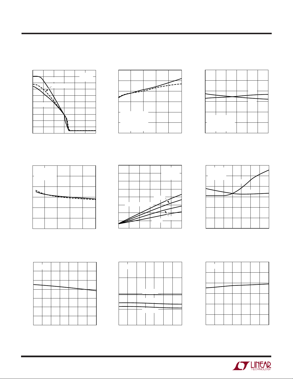
TYPICAL PERFORMANCE CHARACTERISTICS
Gain Characteristics
5.0
4.5
4.0
3.5
3.0
2.5
2.0
1.5
OUTPUT VOLTAGE (V)
1.0
0.5
0
TA = 125°C
TA = 25°C
TA = –55°C
–3
–2
–1
DIFFERENTIAL INPUT VOLTAGE (mV)
Propagation Delay vs
Input Overdrive
12
TA = 25°C
= 100mV
V
STEP
10
= ±5V
V
S
8
6
TIME (ns)
4
2
0
10 20 30 40
0
OVERDRIVE (mV)
01
t
PDLH
t
PDHL
VS = ±5V
= 0
I
OUT
2
1394 G01
1394 TA02
Propagation Delay vs
Load Capacitance
12
10
8
6
TIME (ns)
4
I
= 0
OUT
V
= ±5V
S
= 25°C
T
A
2
= 100mV
V
STEP
OVERDRIVE = 5mV
0
10 20 30 40
3
0
OUTPUT LOAD CAPACITANCE (pF)
t
PDLH
t
PDHL
50
1394 G02
Propagation Delay vs
Source Resistance
80
70
60
50
40
TIME (ns)
50
30
20
10
0
0 0.5
STEP SIZE = 800mV
1.0 2.01.5
SOURCE RESISTANCE (kΩ)
400mV
100mV
VS = ±5V
= 20mV
V
OD
= 25°C
T
A
200mV
2.5
3.0
1394 G04
Propagation Delay vs
Positive Supply Voltage
Propagation Delay vs
Temperature
12
VS = ±5V
= 100mV
V
STEP
10
= 5mV
V
OD
8
6
TIME (ns)
4
2
0
–50
–25 0
TEMPERATURE (°C)
t
PDLH
t
PDHL
50 100 125
25 75
1394 G05
Input Offset Voltage vs
Temperature
2
VS = ±5V
1
0
–1
–2
VOLTAGE (mV)
–3
–4
–5
–50 25 75
–25 0
TEMPERATURE (°C)
4
50 100 125
LT1394 G06
Input Bias Current vs
Temperature
4
VS = ±5V
3
2
1
INPUT BIAS CURRENT (µA)
0
–50 25 75
–25 0
VCM = –5V
VCM = 0V
VCM = 3.5V
TEMPERATURE (°C)
50 100 125
LT1394 G07
Positive Common Mode Limit vs
Temperature
6
VS = ±5V
5
4
3
VOLTAGE (V)
2
1
0
–50
–25 0
TEMPERATURE (°C)
50 100 125
25 75
1394 G08
Page 5
W
U
TYPICAL PERFORMANCE CHARACTERISTICS
LT1394
Negative Common Mode Limit vs
Temperature
1
0
–1
–2
–3
INPUT VOLTAGE (V)
–4
–5
–6
–50 25 75
–25 0
VS = SINGLE 5V
VS = ±5V
50 100 125
TEMPERATURE (°C)
Positive Supply Current vs
V+ Supply Voltage
10
V– = 0V
9
= –60mV
V
IN
= 0
I
8
OUT
7
6
TA = 125°C
5
4
TA = 25°C
CURRENT (mA)
3
2
1
0
0
13
2
TA = –55°C
4
SUPPLY VOLTAGE (V)
5
Output Low Voltage (VOL) vs
Output Sink Current
0.8
VS = ±5V
LT1394 G09
0.7
0.6
0.5
0.4
VOLTAGE (V)
0.3
0.2
0.1
= 30mV
∆V
IN
TA = 125°C
TA = –55°C
0
02 6 10 14
4
OUTPUT SINK CURRENT (mA)
TA = 25°C
8
12
16
1394 G10
Positive Supply Current vs
Switching Frequency
16
VS = ±5V
14
12
10
TA = 125°C
8
6
CURRENT (mA)
TA = –55°C
4
2
0
7
6
8
1394 G12
1
SWITCHING FREQUENCY (MHz)
TA = 25°C
10 100
1394 G13
Output High Voltage (VOH) vs
Output Source Current
5.0
VS = ±5V
4.5
4.0
3.5
3.0
2.5
OUTPUT VOLTAGE (V)
2.0
1.5
1.0
= –30mV
∆V
IN
TA = 125°C
TA = 25°C
TA = –55°C
02 6 10 14
4
OUTPUT SOURCE CURRENT (mA)
8
Negative Supply Current vs
V– Supply Voltage
4
+
V
= 5V
∆V
= –60mV
IN
3
2
CURRENT (mA)
1
0
–7 –5 –3
–8
TA = 125°C
TA = 25°C
TA = –55°C
–6
NEGATIVE SUPPLY VOLTAGE (V)
–4
–1
16
1394 G11
0
1394 G14
12
–2
Latch Pin Current vs Temperature
8
VS = ±5V
7
6
5
4
3
CURRENT (µA)
2
1
0
= 0V
V
LATCH
–50 25 75
–25 0
TEMPERATURE (°C)
50 100 125
LT1394 G15
Response to 100MHz ±10mV
Sine Wave
+IN
20mV
P-P
3V
Q
OUT
0V
FET PROBES 5ns/DIV
10mV/DIV
1V/DIV
1394 G16
5
Page 6

LT1394
W
U
TYPICAL PERFORMANCE CHARACTERISTICS
+
t
Response Time to
PD
5mV Overdrive
1.4V
+IN
5mV
–95mV
V
= ±5V 2ns/DIV
S
= 2MHz
f
IN
V
= 5mV 1394 G17
OD
Q OUT
0V
UUU
PIN FUNCTIONS
V+ (Pin 1): Positive Supply Voltage. Normally 5V.
+IN (Pin 2): Noninverting Input.
–IN (Pin 3): Inverting Input.
V– (Pin 4): Negative Supply Voltage. Normally either 0V or
– 5V.
–
t
Response Time to
PD
5mV Overdrive
1.4V
5mV
+IN
–95mV
VS = ±5V 2ns/DIV
= 2MHz
f
IN
V
= 5mV 1394 G18
OD
Q OUT
0V
GND (Pin 6): Ground.
Q OUT (Pin 7): Noninverting Logic Output. This pin is high
when +IN is above –IN and LATCH ENABLE is low.
Q OUT (Pin 8): Inverting Logic Output. This pin is low
when +IN is above –IN and LATCH ENABLE is low.
LATCH ENABLE (Pin 5): Latch Control Pin. When high, the
outputs remain in a latched condition, independent of the
current state of the inputs.
UW
W
TI I G DIAGRA S
V
OD
∆V
V
IN
V
OUT
IN
t
PD
1394 TD01
LATCH
ENABLE
V
V
OUT
t
SU
IN
t
H
t
L
PD
1394 TD02
6
Page 7

LT1394
U
WUU
APPLICATIONS INFORMATION
Common Mode Considerations
The LT1394 is specified for a common mode range of – 5V
to 3.5V on a ±5V supply or a common mode range of 0V
to 3.5V on a single 5V supply. A more general consideration is that the common mode range is 0V below the
negative supply and 1.5V below the positive supply, independent of the actual supply voltage. The criterion for
common mode limit is that the output still responds
correctly to a small differential input signal.
When either input signal falls below the negative common
mode limit, the internal PN diode formed with the substrate can turn on, resulting in significant current flow
through the die. An external Schottky clamp diode
between the input and the negative rail can speed up
recovery from negative overdrive by preventing the substrate diode from turning on. The zero-crossing detector
in Figure 1 demonstrates the use of a fast clamp diode.
The zero-crossing detector terminates the transmission
line at its 50Ω characteristic impedance. Negative inputs
should not fall below – 2V to keep the signal current within
the clamp diode’s maximum forward rating. Positive
inputs should not exceed the device’s absolute maximum
ratings or the power rating on the terminating resistor.
Either input may go above the positive common mode
limit without damaging the comparator. The upper voltage
limit is determined by an internal diode from each input to
the positive supply. The input may go above the positive
supply as long as it does not go far enough above it to
conduct more than 10mA. Functionality will continue if the
remaining input stays within the allowed common mode
range. There will, however, be an increase in propagation
delay as the input signal switches back into the common
mode range.
+
LT1394
–
5V
Q
Q
1394 F01
R
S
50Ω
V
IN
CABLE
R
1N5712
Figure 1. Fast Zero-Crossing Detector
T
50Ω
Input Bias Current
Input bias current is measured with the output held at
1.4V. As with any PNP differential input stage, the LT1394
bias current flows out of the device. It will go to zero on an
input which is high and double on an input which is low.
LATCH Pin Dynamics
The LATCH pin is intended to retain input data (output
latched) when the LATCH pin goes high. The pin will float
to a high state when disconnected, so a flow-through
condition requires that the LATCH pin be grounded. The
LATCH pin is designed to be driven with either a TTL or
CMOS output. It has no built-in hysteresis.
To guarantee data retention, the input signal must remain
valid at least 2ns after the latch goes high (hold time), and
must be valid at least –0.4ns before the latch goes high
(setup time). The negative setup time simply means that
the data arriving 0.4ns after (rather than before) the latch
signal is valid. When the latch signal goes low, new data
will appear at the output in approximately 6ns (latch
propagation delay).
Measuring Response Time
To properly measure the response of the LT1394 requires
an input signal source with very fast rise times and
exceptionally clean settling characteristics. The last
requirement comes about because the standard comparator test calls for an input step size that is large compared
to the overdrive amplitude. Typical test conditions are
100mV step size with 5mV overdrive. This requires an
input signal that settles to within 1% (1mV) of final value
in only a few nanoseconds with no ringing or settling tail.
Ordinary high speed pulse generators are not capable of
generating such a signal, and in any case, no ordinary
oscilloscope is capable of displaying the waveform to
check its fidelity. Some means must be used to inherently
generate a fast, clean edge with known final value. The
circuit shown in Figure 2 is the best electronic means of
generating a fast, clean step to test comparators. It uses
a very fast transistor in a common base configuration. The
transistor is switched off with a fast edge from the generator and the collector voltage settles to exactly 0V in just a
few nanoseconds. The most important feature of this
7
Page 8

LT1394
U
WUU
APPLICATIONS INFORMATION
0V
25Ω
25Ω
10k
V1**
–100mV
–3V
0.1µF
PULSE
IN
0V
50Ω
130Ω
2N3866
750Ω400Ω
–5V
Figure 2. Response Time Test Circuit
circuit is the lack of feedthrough from the generator to the
comparator input. This prevents overshoot on the comparator input, which would give a false fast reading on
comparator response time.
To adjust the circuit for exactly 5mV overdrive, V1 is
adjusted so that the LT1394 output under test settles to
1.4V (in the linear region). Then V1 is changed by –1V to
set overdrive to 5mV.
High Speed Design Techniques
A substantial amount of design effort has made the LT1394
relatively easy to use. It is much less prone to oscillation
than some slower comparators, even with slow input
signals. However, as with any high speed comparator,
there are a number of pitfalls which may arise because of
PC board layout and design. The most common problems
involve power supply bypassing. Bypassing is necessary
to maintain low supply impedance. DC resistance and
inductance in supply wires and PC traces can quickly build
up to unacceptable levels. This allows the supply line to
move with changing internal current levels of the connected devices. This will almost always result in improper
operation. In addition, adjacent devices connected through
an unbypassed supply can interact with each other through
the finite supply impedances. Bypass capacitors furnish a
simple solution to this problem by providing a local
reservoir of energy at the device, keeping supply impedances low.
Bypass capacitors should be as close as possible to the
LT1394. A good high frequency capacitor such as a 0.1µF
0.01µF*
5V
Q
50Ω
+
LT1394
–
–5V
Q
0.01µF
FET PROBE
FET PROBE
* TOTAL LEAD LENGTH INCLUDING DEVICE PIN.
SOCKET AND CAPACITOR LEADS SHOULD BE
LESS THAN 0.5 IN. USE GROUND PLANE
** (V
+ OVERDRIVE)/200
OS
1394 F02
ceramic is recommended, in parallel with a larger capacitor such as a 4.7µF tantalum.
Poor trace routes and high source impedances are also
common sources of problems. Be sure to keep trace
lengths as short as possible, and avoid running any output
trace adjacent to an input trace to prevent unnecessary
coupling. If output traces are longer than a few inches, be
sure to terminate them with a resistor to eliminate any
reflections that may occur. Resistor values are typically
250Ω to 400Ω. Also, be sure to keep source impedances
as low as possible, preferably 1kΩ or less.
Crystal Oscillators
Figure 3’s circuits are crystal oscillators. In the circuit (a)
the resistors at the LT1394’s positive input set a DC bias
point. The 2k-0.068µF path sets up phase shifted feedback
and the circuit looks like a wideband unity-gain follower at
DC. The crystal’s path provides resonant positive feedback and stable oscillation occurs. The circuit (b) is
similar, but supports oscillation frequencies to 30MHz.
Above 10MHz, AT-cut crystals operate in overtone mode.
Because of this, oscillation can occur at multiples of the
desired frequency. The damper network rolls off gain at
high frequency, ensuring proper operation.
Switchable Output Crystal Oscillator
Figure 4 permits crystals to be electronically switched by
logic commands. This circuit is similar to the previous
examples, except that oscillation is only possible when
one of the logic inputs is biased high.
8
Page 9

LT1394
U
WUU
APPLICATIONS INFORMATION
5V
2k
(a)
(b)
22Ω
820pF
2k
5V
2k
2k
Figure 3. Crystal Oscillators for Outputs to 30MHz. Circuit (b)’s
Damper Network Supresses Overtone Crystal’s Harmonic Modes
XTAL X
XTAL B
5V
1k
XTAL A
+
1k
LT1394
–
75pF
= 1N4148
GROUND XTAL CASES
Figure 4. Switchable Output Crystal Oscillator. Biasing A or B
High Places Associated Crystal in Feedback Path. Additional
Crystal Branches Are Permissible
1MHz TO 10MHz
CRYSTAL (AT-CUT)
+
LT1394
–
0.068µF
10MHz TO 25MHz
CRYSTAL (AT-CUT)
+
LT1394
–
200pF
D2
D1
2k
OUTPUT
2k
OUTPUT
2k
1394 F03
R
LOGIC INPUTS
X
AS MANY STAGES
D
X
AS DESIRED
1k
B
1k
A
OUTPUT
1394 F04
Temperature-Compensated Crystal Oscillator (TXCO)
Figure 5 is a temperature-compensated crystal oscillator
(TXCO). This circuit reduces oscillator temperature drift
by inserting a temperature-dependent compensatory correction into the crystal’s frequency trimming network.
This open-loop correction technique relies on cancellation
of the temperature characteristics of the oscillator, which
are quite repeatable.
The LT1394 and associated components form the crystal
oscillator, operating similarly to Figure 3’s examples. The
LM134, a temperature-dependent current source, biases
A1. A1 takes gain referred to the LM134’s output and the
negative offset supplied via the 470kΩ-LT1004 reference
path. Note that the LT1004’s negative voltage bias is
bootstrapped from the oscillator’s output, maintaining
single supply operation. This arrangement delivers temperature-dependent bias to the varactor diode, causing a
scaled variation in the crystal’s resonance versus ambient
temperature. The varactor’s bias-dependent capacitance
shift pulls crystal frequency to complement the circuit’s
temperature drift. The simple first order fit provided by the
compensation is very effective. Figure 6 shows results.
The –70ppm frequency shift over 0°C to 70°C is corrected
within a few ppm. The “FREQ SET” trim also biases the
varactor, allowing accurate output frequency setting. It is
worth noting that better compensation is possible by
including higher order terms in the temperature-to-voltage conversion.
18ns, 500µV Sensitivity Comparator
The ultimate limitation on comparator sensitivity is available gain. Unfortunately, increasing gain invariably
involves giving up speed. The gain vs. speed trade-off in a
fast comparator is usually a practical compromise
designed to satisfy most applications. Some situations,
however, require more sensitivity (e.g., higher gain) with
minimal impact on speed. Figure 7’s circuit adds a differential preamplifier ahead of the LT1394, increasing gain.
This permits 500µV comparisons in 18ns. A parallel path
DC stabilization approach eliminates preamplifier drift as
an error source. A1 is the differential preamplifier, operating at a gain of 100. Its output is AC-coupled to the LT1394.
9
Page 10

LT1394
U
WUU
APPLICATIONS INFORMATION
0.01µF
+
–
0.068µF
MV-209
VARACTOR
DIODE
LT1394
2k
2M
10MHz
1µF
10M
2k
5V
390Ω
XTAL AT-CUT, 35° 25′ ANGLE
* 1% FILM RESISTOR
2M
0.01µF
4.7k
BAT-85
5.8M*
A1
LT1077
+
1µF
–
+
50k
1M*
1M*
470k*
LT1004-1.2
226Ω*
100k
1M
FREQ SET
5V
LM134
10mV/°C
10k*
10MHz
0.05ppm/°C
1394 F05
Figure 5. Temperature-Compensated 10MHz Crystal Oscillator.
Temperature-Dependent Varactor Bias Reduces Drift by 20:1
0
–10
–20
–30
–40
–50
–60
FREQUENCY DEVIATION (ppm)
–70
0
UNCOMPENSATED
(VARACTOR CORRECTION
DISABLED) –1ppm/°C
10 20
TEMPERATURE (°C)
COMPENSATED
≈ 0.05ppm/°C
40 60 70
30 50
1394 F06
Figure 6. Figure 5’s Compensated vs Uncompensated
Temperature Dependence. First Order Compensation
Reduces Oscillator Drift to 0.05ppm/°C
200pF
+INPUT
–INPUT
5V
+
A2
2k
1/2 LT1126
–
–
A3
1/2 LT1126
10k
200Ω
10k
+
200pF
+
LM733
A = 100
–
–5V
5V
+
A1
1µF
1k
+
LT1394
–
OUTPUT
2k
–
1µF
–5V
1k
1394 F07
10
Figure 7. Parallel Preamplified Paths Allow 18ns Comparator
Response to 500µV Overdrive
Page 11

LT1394
U
WUU
APPLICATIONS INFORMATION
A1 has poorly defined DC characteristics, necessitating
some form of DC correction. A2 and A3, operating at a
differential gain of 100, provide this function. They differentially sense a band limited version of A1’s inputs and feed
DC and low frequency amplified information to the comparator. The low frequency roll-off of A1’s signal path
complements A2-A3’s high frequency roll-off. The summation of these two signal channels at the LT1394 inputs
results in flat response from DC to high frequency.
Figure 8 shows waveforms for the high gain comparator.
Trace A is a 500µV overdrive on a 1mV step applied to the
circuit’s positive input (negative input grounded). Trace B
shows the resulting amplified step at A1’s positive output.
Trace C is A2’s band limited output. A1’s wideband output
combines with A2’s DC corrected information to yield the
A = 1mV/DIV
B = 0.1V/DIV
(AC-COUPLED)
C = 0.1V/DIV
correct, amplified composite signal at the LT1394’s positive input in Trace D. The LT1394’s output is Trace E. Figure
9 details circuit propagation delay. The output responds in
18ns to a 500µV overdrive on a 1mV step. Figure 10 plots
response time versus overdrive. As might be expected,
propagation delay decreases at higher overdrives. A1’s
noise limits usable sensitivity.
1100
1000
900
800
OVERDRIVE (µV)
700
600
500
15
Figure 10. Response Time vs Overdrive for the
Composite Comparator
16 17 18
RESPONSE TIME (ns)
1394 F10
D = 0.1V/DIV
E = 5V/DIV
5µs/DIV 1394 F08
Figure 8. 500µV Input (Trace A) Is Split into Wideband
and Low Frequency Gain Paths (Traces B and C) and
Recombined (Trace D). Comparator Output Is Trace E
A = 1mV/DIV
B = 1V/DIV
10ns/DIV 1394 F09
Figure 9. Parallel Path Comparator Shows 18ns
Response (Trace B) to 500µV Overdrive (Trace A)
Voltage-Controlled Delay
The ability to set a precise, predictable delay has broad
application in pulse circuitry. Figure 11’s configuration
sets a 0 to 300ns delay from a corresponding 0V to 3V
control voltage. It takes advantage of the LT1394’s speed
and the clean dynamics of an emitter switched current
source.
Q1 and Q2 form a current source that charges the 1000pF
capacitor. When the trigger input is high (Trace A, Figure
12) both Q3 and Q4 are on. The current source is off and
Q2’s collector (Trace B) is at ground. The latch input at the
LT1394 prevents it from responding and its output remains
high. When the trigger input goes low, the LT1394’s latch
input is disabled and its output drops low. Q4’s collector
(Trace C) lifts and Q2 comes on, delivering constant
current to the 1000pF capacitor (Trace B). The resulting
linear ramp at the LT1394’s positive input is compared to
the delay programming voltage input. When a crossing
occurs, the comparator goes high (Trace D). The length of
time the comparator was low is directly proportional to the
11
Page 12

LT1394
U
WUU
APPLICATIONS INFORMATION
0.1µF
5V
Q2
100Ω
100Ω
(DELAY
CALIB)
Q4
LT1634
Q1
1000pF
220Ω
PNP = 2N5087
NPN = 2N2369
Figure 11. Fast, Precise, Voltage-Controlled Delay.
Emitter Switched Current Source Has Clean,
Predictable Dynamics
DELAY PROGRAMMING
VOLTAGE INPUT
0V TO 3V = 0 TO 300ns DELAY
51pF
330Ω
Q3
330Ω
TRIGGER INPUT
200ns MINIMUM
1k
0.1µF
–
LT1394
+
Q OUTPUT
Q OUTPUT
1394 F11
A = 5V/DIV
B = 2V/DIV
C = 5V/DIV
D = 5V/DIV
100ns/DIV
1394 F12
Figure 12. Voltage-Controlled Delay’s Waveforms.
Programming Voltage Determines Delay Between Input
(Trace A) Falling Edge and Output (Trace D) Rising Edge.
High Linearity Timing Ramp (Trace B) Permits 1ns
Accuracy and 100ps Repeatability
A = 2V/DIV
B = 0.1V/DIV
C = 2V/DIV
D = 2V/DIV
delay programming voltage. The fast switching and ramp
linearity permits 1ns accuracy and 100ps repeatability.
Figure 13, a high speed expansion of the current source
turn-on, details the clean switching. Q4 goes off within 2ns
of the trigger input (Trace A) dropping low, enabling the
current source (Q2’s emitter is Trace C). Concurrently, the
1000pF capacitor’s ramp (Trace B) begins. The LT1394’s
output (Trace D) drops low about 7ns later, returning high
after crossing (in this case) a relatively low programming
voltage. Figure 14 juxtaposes the waveforms differently,
permitting enhanced study of circuit timing. Switching
begins with the input trigger falling low (Trace A). The ramp
(Trace C) begins 3ns after the current source turns on (Q2
emitter is Trace D). The output pulse (Trace B) begins
about 4ns later.
To calibrate this circuit apply a trigger input and 3V to the
programming input. Adjust the 100Ω trim for a 300ns
width at the LT1394’s output.
10ns/DIV 1394 F13
Figure 13. High Speed Expansion of Figure 12. Ramp
(Trace B) Begins When Trigger (Trace A) Falls and
Current Source Turns On (Trace C). Trace D is Output
A = 1V/DIV
B = 1V/DIV
C = 0.1V/DIV
D = 1V/DIV
10ns/DIV 1394 F14
Figure 14. Delay’s Output Switching Begins with
Trigger Falling Low (Trace A). Ramp (Trace C) Starts
3ns After Current Source Turn-On (Trace D). Output
(Trace B) Begins 4ns Later
12
Page 13

LT1394
U
WUU
APPLICATIONS INFORMATION
Fast, High Impedance, Variable Threshold Trigger
A frequent requirement in instrumentation is a fast trigger
with a variable threshold. Often, a high impedance input is
also required. Figure 15 meets these requirements. Comparator C1 is the basic trigger, with threshold voltage set at
its negative input. Source follower Q1 provides high
impedance with about 2pF input capacitance and 50pA bias
current. Normally, Q1’s source bias point would be uncertain and drifty, but stabilization techniques eliminate this
concern. A1 measures filtered versions of Q1’s gate and
source voltages. A1’s output biases Q2, forcing Q1’s
channel current to whatever value is required to equalize
A1’s inputs, and hence Q1’s gate and source voltages. A1’s
input filtering and roll-off are far slower than input frequencies of interest; its action does not interfere with the
circuit’s main signal path. The 330pF capacitor prevents
fast edges coupled through Q2’s collector base junction
from influencing A1’s operation.
Q1 should contribute negligible timing error to minimize
overall delay. Figure 16’s photo verifies Q1’s wideband
operation. Trace B, Q1’s source, lags the input (Trace A) by
only 300ps. Input, FET buffer output and C1 output appear
as Traces A, B and C, respectively in Figure 17. As before,
the FET buffer is seen to contribute small timing error, and
C1’s output is about 8ns delayed from the input.
A = 1V/DIV
B = 1V/DIV
200ps/DIV 1394 F16
V
TRIG
±3V
–
LT1394
C1
OUTPUT
INPUT
±3V
5V
Q1
2N5486
+
10M
10M
0.1µF
1394 F15
Q2
2N3904
100Ω
–5V
1.5k
330pF
0.01µF
A1
LT1097
10k
–
+
0.1µF
Figure 15. Buffer Provides 2pF, 50pA Input Characteristics for
Fast Trigger. Amplifier-Stabilized Biasing Eliminates FET Offset
Figure 16. Trigger Buffer’s 300ps Delay Minimizes
Timing Error. 4GHz Sampling Oscilloscope’s Output Is
a Series of Dots
C = 2V/DIV
A = 1V/DIV
B = 1V/DIV
10ns/DIV 1394 F17
Figure 17. Input (Trace A), FET Source (Trace B)
and Output (Trace C) Waveforms for the Trigger.
Total Delay Is 8ns
13
Page 14

LT1394
U
WUU
APPLICATIONS INFORMATION
High Speed Adaptive Trigger Circuit
Line and fibre-optic receivers often require an adaptive
trigger to compensate for variations in signal amplitude
and DC offsets. The circuit in Figure 18 triggers on 2mV to
175mV signals from 100Hz to 45MHz while operating from
a single 5V rail. A1, operating at a gain of 15, provides
wideband AC gain. The output of this stage biases a 2-way
peak detector (Q1 through Q4). The maximum peak is
stored in Q2’s emitter capacitor, while the minimum excursion is retained in Q4’s emitter capacitor. The DC value of
the midpoint of A1’s output signal appears at the junction
of the 500pF capacitor and the 3MΩ units. This point
always sits midway between the signal’s excursions,
egardless of absolute amplitude. This signal-adaptive voltage is buffered by A2 to set the trigger voltage at the
LT1394’s positive input. The LT1394’s negative input is
biased directly from A1’s output. The LT1394’s output, the
circuit’s output, is unaffected by >85:1 signal amplitude
variations. Bandwidth limiting in A1 does not affect triggering because the adaptive trigger threshold varies
ratiometrically to maintain circuit output.
Figure 19 shows operating waveforms at 45MHz. Trace A’s
input produces Trace B’s amplified output at A1. The
comparator’s output is Trace C.
Split supply versions of this circuit can achieve bandwidths to 50MHz with wider input operating range.
A = 0.1V/DIV
B = 0.1V/DIV
C = 5V/DIV
AN72 F64
50ns/DIV
Figure 19. Adaptive Trigger Responding to a 40MHz,
5mV Input. Input Amplitude Variations from 2mV to
175mV Are Accommodated
10µF
5V
2k
1
0.005µF
14
2k
6
5
3M
4
500pF
0.005µF
10
12
11
3M
Q4
+
LT1006
–
5V
A2
Q1, Q2, Q3, Q4 = CA3096 ARRAY:
TIE SUBSTRATE (PIN 16) TO GROUND
= 1N4148
470Ω
+
470Ω
0.1µF
LT1394
–
TRIGGER
OUT
1394 F18
3
Q1 Q2
+
LT1227
5V
A1
2
–
750Ω
2k
5V
+
+
0.1µF
INPUT
36Ω
100µF
510Ω
0.1µF
13
Q3
15
Figure 18. 45MHz Single Supply Adaptive Trigger. Output Comparator’s
Threshold Varies Ratiometrically with Input Amplitude, Maintaining Data
Integrity over >85:1 Input Amplitude Range
14
Page 15

PACKAGE DESCRIPTION
(
U
Dimensions in inches (millimeters) unless otherwise noted.
MS8 Package
8-Lead Plastic MSOP
(LTC DWG # 05-08-1660)
0.118 ± 0.004*
(3.00 ± 0.102)
8
7
6
5
LT1394
0.192 ± 0.004
(4.88 ± 0.10)
12
0.040
± 0.006
SEATING
PLANE
(1.02 ± 0.15)
0.012
(0.30)
0.0256
REF
(0.65)
0.152mm) PER SIDE
TYP
0.007
(0.18)
0.021
± 0.006
(0.53 ± 0.015)
* DIMENSION DOES NOT INCLUDE MOLD FLASH, PROTRUSIONS OR GATE BURRS. MOLD FLASH,
PROTRUSIONS OR GATE BURRS SHALL NOT EXCEED 0.006" (0.152mm) PER SIDE
** DIMENSION DOES NOT INCLUDE INTERLEAD FLASH OR PROTRUSIONS.
INTERLEAD FLASH OR PROTRUSIONS SHALL NOT EXCEED 0.006"
° – 6° TYP
0
0.118 ± 0.004**
4
3
(3.00 ± 0.102)
0.034 ± 0.004
(0.86 ± 0.102)
S8 Package
8-Lead Plastic Small Outline (Narrow 0.150)
(LTC DWG # 05-08-1610)
0.189 – 0.197*
(4.801 – 5.004)
7
8
6
0.006 ± 0.004
(0.15 ± 0.102)
MSOP (MS8) 1197
5
0.228 – 0.244
(5.791 – 6.197)
1
2
0.010 – 0.020
(0.254 – 0.508)
0.008 – 0.010
(0.203 – 0.254)
*
DIMENSION DOES NOT INCLUDE MOLD FLASH. MOLD FLASH
SHALL NOT EXCEED 0.006" (0.152mm) PER SIDE
**
DIMENSION DOES NOT INCLUDE INTERLEAD FLASH. INTERLEAD
FLASH SHALL NOT EXCEED 0.010" (0.254mm) PER SIDE
Information furnished by Linear Technology Corporation is believed to be accurate and reliable.
However, no responsibility is assumed for its use. Linear Technology Corporation makes no representation that the interconnection of its circuits as described herein will not infringe on existing patent rights.
0.016 – 0.050
0.406 – 1.270
× 45°
0.053 – 0.069
(1.346 – 1.752)
0°– 8° TYP
0.014 – 0.019
(0.355 – 0.483)
0.150 – 0.157**
(3.810 – 3.988)
3
4
0.004 – 0.010
(0.101 – 0.254)
0.050
(1.270)
TYP
SO8 0996
15
Page 16

LT1394
U
TYPICAL APPLICATION
Voltage-Controlled Crystal Oscillator (VCXO)
Figure 20, a variant of the basic crystal oscillator, permits
voltage tuning the output frequency. Such voltage-controlled crystal oscillators (VCXO) are often employed
where slight variation of a stable carrier is required. This
example is specifically intended to provide a 4× NTSC
sub-carrier tunable oscillator suitable for phase locking.
The LT1394 is set up as a crystal oscillator, operating
similarly to Figure 3 (a). The varactor diode is biased from
the tuning input. The tuning network is arranged so a 0V
to 5V drive provides a reasonably symmetric, broad tuning
range around the 14.31818MHz center frequency. The
indicated selected capacitor sets tuning bandwidth. It
should be picked to complement loop response in phase
locking applications. Figure 21 is a plot of tuning input
voltage versus frequency deviation. Tuning deviation from
the 4× NTSC 14.31818MHz center frequency exceeds
±240ppm for a 0V to 5V input.
1N4148
1M
1M
5V
MV-209
C SELECT***
0.047µF
†
1M*
1M
9
8
7
6
5
14.31818MHz
4
3
2
FREQUENCY DEVIATION (kHz)
1
14.314.0MHz
0
0
13
INPUT VOLTAGE (V)
14.3217MHz
5
2
4
1394 F21
Figure 21. Control Voltage vs Output Frequency for Figure 15.
Tuning Deviation from Center Frequency Exceeds ±240ppm
5V
47k*
LT1004-2.5
1k*
3.9k*
V
IN
0V TO 5V
100pF
2k
390Ω
200pF
+
LT1394
–
Y1**
15pF
2k
100pF
* 1% FILM RESISTOR
** NORTHERN ENGINEERING LABS C-2350N-14.31818MHz
*** C SELECT SETS TUNING BANDWIDTH. SET TO COMPLEMENT
LOOP RESPONSE IN PHASE LOCKING APPLICATIONS
†
VARACTOR DIODE
FREQUENCY
OUTPUT
1394 F20
Figure 20. A 4× NTSC Sub-Carrier Voltage-Tunable Crystal Oscillator. Tuning Range
and Bandwidth Accommodate Variety of Phase Locked Loops
RELATED PARTS
PART NUMBER DESCRIPTION COMMENTS
LT1016 UltraFast Precision Comparator Industry Standard 10ns Comparator
LT1116 12ns Single Supply Ground-Sensing Comparator Single Supply Version of LT1016
LT1671 Fast Single Supply Comparator 60ns, 450µA Single Supply Comparator
LT1720 UltraFast Dual Single Supply Comparator Dual 4.5ns, 4mA Single Supply Comparator
1394f LT/TP 0499 4K • PRINTED IN USA
LINEAR TECHNOLOGY CORPORATION 1998
16
Linear Technology Corporation
1630 McCarthy Blvd., Milpitas, CA 95035-7417
(408) 432-1900 ● FAX: (408) 434-0507
●
www.linear-tech.com
 Loading...