

Page 1
FEATURES
LT1389
Nanopower Precision
Shunt Voltage Reference
U
DESCRIPTIO
■
Initial Voltage Accuracy: 0.05%
■
Low Operating Current: 800nA
■
Low Drift: 10ppm/°C Max
■
Less Than 1Ω Dynamic Impedance
■
Available in 1.25V, 2.5V, 4.096V and
5V SO-8 Packages
U
APPLICATIO S
■
Portable Meters
■
Precision Regulators
■
A/D and D/A Converters
■
Calibrators
TYPICAL APPLICATIO
The LT®1389 is a nanopower, precision shunt voltage
reference. The bandgap reference uses trimmed precision thin-film resistors and improved curvature correction
techniques to achieve 0.05% initial voltage accuracy with
guaranteed 10ppm/°C maximum temperature drift. Voltage regulation is maintained to an ultralow 800nA operating
current. Advances in design, processing and packaging
achieve low temperature cycling hysteresis.
The LT1389 does not require an output compensation
capacitor, but is stable with capacitive loads. Low dynamic impedance makes the LT1389 reference easy to
use from unregulated supplies.
The LT1389 reference can be used as a high performance
upgrade to the LM185/LM385, LT1004, LT1034 and
LT1634 where lowest power and guaranteed temperature drift are required.
, LTC and LT are registered trademarks of Linear Technology Corporation.
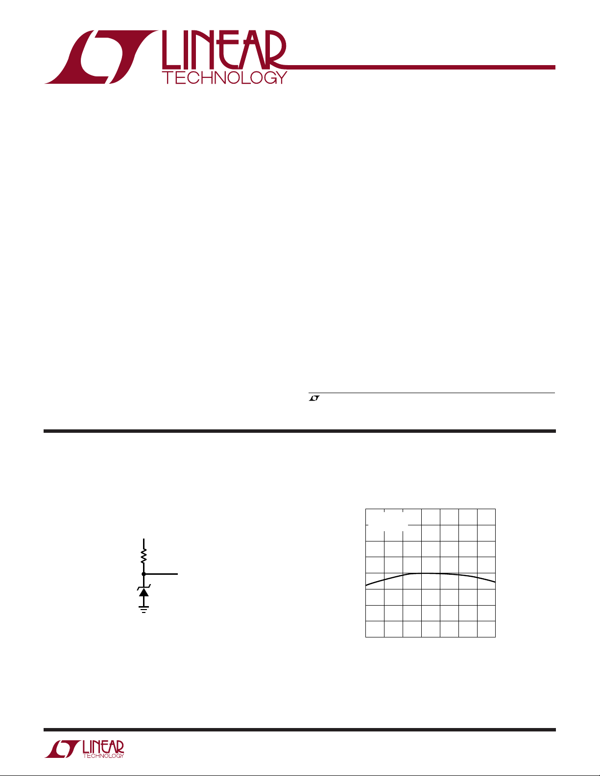
U
5V
4.7M
LT1389-1.25
V
OUT
1.25V
1389 TA01
Temperature Drift
2.0
IR = 0.8µA
= 1.25V
V
1.5
OUT
1.0
0.5
0
–0.5
–1.0
–1.5
REFERENCE VOLTAGE CHANGE (mV)
–2.0
10 20 40
0
30
TEMPERATURE (°C)
50 60
70
1389 TA02
1
Page 2
LT1389
PACKAGE/ORDER I FOR ATIO
UU
W
WWWU
ABSOLUTE AXI U RATI GS
(Note 1)
Operating Current
1.25V............................................................... 20mA
2.5V................................................................. 20mA
4.096V............................................................. 10mA
5V.................................................................... 10mA
Forward Current .................................................. 20mA
Operating Temperature Range ..................... 0°C to 70°C
Storage Temperature Range (Note 2) ... –65°C to 150°C
Lead Temperature (Soldering, 10 sec).................. 300°C
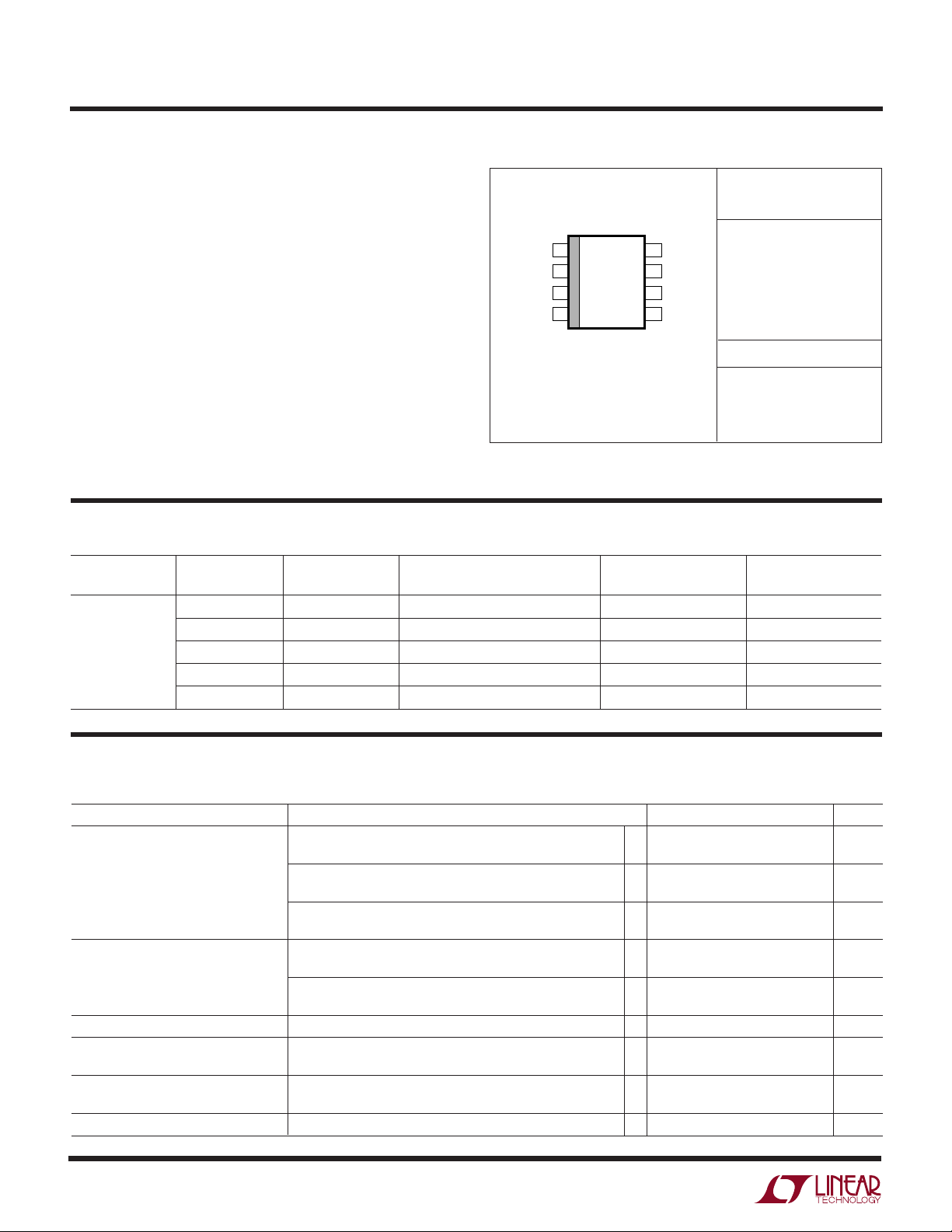
U
AVAILABLE OPTIO S
ORDER PART
NUMBER
1
DNC*
2
DNC*
3
DNC*
4
GND
8-LEAD PLASTIC SO
T
= 125°C, θJA = 190°C/W
JMAX
TOP VIEW
S8 PACKAGE
8
DNC*
7
DNC*
6
V
OUT
5
GND
LT1389ACS8-1.25
LT1389BCS8-1.25
LT1389BCS8-2.5
LT1389BCS8-4.096
LT1389BCS8-5
S8 PART MARKING
389A12
389B12
1389B4
1389B5
389B25
*Connected internally. Do Not Connect external circuitry to these pins.
Consult factory for Industrial and Military grade parts.
OUTPUT
TEMPERATURE VOLTAGE ACCURACY (%) (ppm/°C) PART TYPE PART MARKING
0°C to 70°C 1.250 0.05 10 LT1389ACS8-1.25 389A12
1.250 0.05 20 LT1389BCS8-1.25 389B12
2.500 0.05 20 LT1389BCS8-2.5 389B25
4.096 0.075 50 LT1389BCS8-4.096 1389B4
5.000 0.075 50 LT1389BCS8-5 1389B5
1.25V ELECTRICAL CHARACTERISTICS
temperature range, otherwise specifications are at TA = 25°C. (Note 3)
PARAMETER CONDITIONS MIN TYP MAX UNITS
Reverse Breakdown Voltage LT1389ACS8/LT1389BCS8 (IR = 0.8µA) 1.24937 1.250 1.25062 V
LT1389ACS8 (IR = 0.8µA) ● 1.24849 1.250 1.25149 V
LT1389BCS8 (IR = 0.8µA) ● 1.24762 1.250 1.25237 V
Reverse Breakdown Change 0.8µA ≤ IR ≤ 200µA 0.20 0.4 mV
with Current (Note 4)
200µA ≤ IR ≤ 2mA 0.3 1.0 mV
Minimum Operating Current ● 0.6 µA
Temperature Coefficient LT1389ACS8 (IR = 0.8µA) ● 4 10 ppm/°C
LT1389BCS8 (I
Reverse Dynamic Impedance (Note 5) 0.8µA ≤ IR ≤ 2mA 0.25 0.7 Ω
Low Frequency Noise (Note 6) IR = 0.8µA, 0.1Hz ≤ f ≤ 10Hz 25 µV
TEMPERATURE COEFFICIENT
The ● denotes specifications which apply over the full operating
–0.05 0.05 %
–0.12 0.12 %
–0.19 0.19 %
● 0.20 1.0 mV
● 0.3 2.0 mV
= 0.8µA) ● 4 20 ppm/°C
R
● 0.25 1.5 Ω
P-P
2
Page 3
LT1389
2.5V ELECTRICAL CHARACTERISTICS
temperature range, otherwise specifications are at TA = 25°C. (Note 3)
PARAMETER CONDITIONS MIN TYP MAX UNITS
Reverse Breakdown Voltage LT1389BCS8 (IR = 0.9µA) 2.49875 2.500 2.50125 V
LT1389BCS8 (IR = 0.9µA) ● 2.49525 2.500 2.50475 V
Reverse Breakdown Change 0.9µA ≤ IR ≤ 200µA 0.2 0.5 mV
with Current (Note 4)
200µA ≤ IR ≤ 2mA 0.3 1.0 mV
Minimum Operating Current ● 0.7 µA
Temperature Coefficient IR = 0.9µA ● 8 20 ppm/°C
Reverse Dynamic Impedance (Note 5) 0.9µA ≤ IR ≤ 2mA 0.25 0.75 Ω
Low Frequency Noise (Note 6) IR = 0.9µA, 0.1Hz ≤ f ≤ 10Hz 50 µV
4.096V ELECTRICAL CHARACTERISTICS
operating temperature range, otherwise specifications are at TA = 25°C. (Note 3)
PARAMETER CONDITIONS MIN TYP MAX UNITS
Reverse Breakdown Voltage LT1389BCS8 (IR = 1.5µA) 4.09293 4.096 4.09907 V
LT1389BCS8 (IR = 1.5µA) ● 4.0788 4.096 4.1132 V
Reverse Breakdown Change 1.5µA ≤ IR ≤ 200µA 0.2 1.5 mV
with Current (Note 4)
200µA ≤ IR ≤ 2mA 0.3 4 mV
Minimum Operating Current ● 1 µA
Temperature Coefficient IR = 1.5µA ● 12 50 ppm/°C
Reverse Dynamic Impedance (Note 5) 1.5µA ≤ IR ≤ 2mA 0.75 2 Ω
Low Frequency Noise (Note 6) IR = 1.5µA, 0.1Hz ≤ f ≤ 10Hz 80 µV
The ● denotes specifications which apply over the full operating
–0.05 0.05 %
–0.19 0.19 %
● 0.2 1.5 mV
● 0.3 2.5 mV
● 0.25 2 Ω
The ● denotes specifications which apply over the full
–0.075 0.075 %
–0.42 0.42 %
● 0.2 3 mV
● 0.3 6 mV
● 0.75 3 Ω
P-P
P-P
3
Page 4
LT1389
5V ELECTRICAL CHARACTERISTICS
temperature range, otherwise specifications are at TA = 25°C. (Note 3)
PARAMETER CONDITIONS MIN TYP MAX UNITS
Reverse Breakdown Voltage LT1389BCS8 (IR = 1.5µA) 4.99625 5.000 5.00375 V
LT1389BCS8 (IR = 1.5µA) ● 4.979 5.000 5.021 V
Reverse Breakdown Change 1.5µA ≤ IR ≤ 200µA 0.2 1.5 mV
with Current (Note 4)
200µA ≤ IR ≤ 2mA 0.3 4 mV
Minimum Operating Current ● 1 µA
Temperature Coefficient IR = 1.5µA ● 12 50 ppm/°C
Reverse Dynamic Impedance (Note 5) 1.5µA ≤ IR ≤ 2mA 0.75 2 Ω
Low Frequency Noise (Note 6) IR = 1.5µA, 0.1Hz ≤ f ≤ 10Hz 100 µV
Note 1: Absolute Maximum Ratings are those values beyond which the life
of a device may be impaired.
Note 2: If the part is stored outside of the specific operating temperature
range, the output may shift due to hysteresis.
Note 3: ESD (Electrostatic Discharge) sensitive device. Use proper ESD
handling precautions.
The ● denotes specifications which apply over the full operating
–0.075 0.075 %
–0.42 0.42 %
● 0.2 3 mV
● 0.3 6 mV
● 0.75 3 Ω
P-P
Note 4: Output requires 0.1µF for operating current greater than 1mA.
Note 5: This parameter is guaranteed by “reverse breakdown change with
current” test.
Note 6: Peak-to-peak noise is measured with a single highpass filter at
0.1Hz and 2-pole lowpass filter at 10Hz.
4
Page 5

UW
FORWARD CURRENT (mA)
0.001
0.4
FORWARD VOLTAGE (V)
0.5
0.6
0.7
0.8
0.01 0.1 1 10 100
1389-1.25 G06
0.3
0.2
0.1
0
0.9
1.0
TA = 25°C
1.25V TYPICAL PERFOR A CE CHARACTERISTICS
Reverse Characteristics
1.0
TA = –40°C TO 85°C
0.8
0.6
0.4
REVERSE CURRENT (µA)
0.2
0
0
0.4
REVERSE VOLTAGE (V)
0.8
1.2
1.6
1389-1.25 G01
Temperature Drift
2.0
1.5
1.0
0.5
0
IR = 250µA
–0.5
–1.0
–1.5
REFERENCE VOLTAGE CHANGE (mV)
–2.0
–40
IR = 0.8µA
–20 0 40
20
TEMPERATURE (°C)
60
1389-1.25 G02
80
Reverse Voltage Change
vs Current
1.2
1.0
0.8
0.6
0.4
0.2
REVERSE VOLTAGE CHANGE (mV)
0
0.001 0.1 101
0.01
REVERSE CURRENT (mA)
LT1389
–40°C
25°C
85°C
1389-1.25 G03
1000
100
10
1
DYNAMIC IMPEDANCE (Ω)
0.1
0.001
25
20
15
10
5
0
–5
–10
NOISE VOLTAGE (µV/DIV)
–15
–20
–25
0
REVERSE CURRENT (mA)
0.10.01 101
0.1Hz to 10Hz Noise
IR = 0.8µA
10
20
30
40
TIME (SEC)
50
TA = 25°C
f = 25Hz
1389-1.25 G04
1389-1.25 G07
Dynamic Impedance vs Frequency
100
TA = 25°C
10
DYNAMIC IMPEDANCE (kΩ)
0.1
0.01
1
0.01
IR = 0.8µA
= 0µF
C
OUT
I
= 10µA
R
= 0µF
C
OUT
0.1 1 10
FREQUENCY (kHz)
C
OUT
= 0.8µA
I
R
= 0.047µF
IR = 10µA
C
OUT
= 0.1µF
1389-1.25 G05
Response Time
1.5V
1V
0.5V
0V
5V
0V
I
= 0.8µA
R
= 0µF
C
OUT
7060
1ms/DIV
1389-1.25 G08
Forward CharacteristicsReverse Dynamic Impedance
Response Time
1.5V
1V
0.5V
0V
5V
0V
I
= 0.8µA
R
= 0.1µF
C
OUT
200ms/DIV
1389-1.25 G09
5
Page 6

LT1389
REVERSE CURRENT (mA)
0.4
REVERSE VOLTAGE CHANGE (mV)
0.8
1.2
0.001 0.1 1 10
1389-2.5 G03
0
1.6
2.0
0.01
–40°C
25°C
85°C
FORWARD CURRENT (mA)
0.001
0.4
FORWARD VOLTAGE (V)
0.5
0.6
0.7
0.8
0.01 0.1 1 10 100
1389-2.5 G06
0.3
0.2
0.1
0
0.9
1.0
TA = 25°C
UW
2.5V TYPICAL PERFOR A CE CHARACTERISTICS
Reverse Characteristics
1000
TA = –40°C TO 85°C
800
Temperature Drift
4.0
3.0
2.0
Reverse Voltage Change
vs Current
600
400
REVERSE CURRENT (nA)
200
1000
DYNAMIC IMPEDANCE (Ω)
100
0.1
0
10
1
0.001
0
0.8
0.4
REVERSE VOLTAGE (V)
REVERSE CURRENT (mA)
1.2
1.6 2.0 2.4 2.8
0.10.01 101
1389-2.5 G01
TA = 25°C
f = 25Hz
1389-2.5 G04
1.0
0
= 250µA
I
R
–1.0
–2.0
REVERSE VOLTAGE CHANGE (mV)
–3.0
–4.0
–40
IR = 0.9µA
0
–20 20
TEMPERATURE (°C)
40 60 80
Dynamic Impedance vs Frequency
100
TA = 25°C
10
IR = 0.9µA
= 0µF
C
DYNAMIC IMPEDANCE (kΩ)
0.1
0.01
1
0.01
OUT
IR = 10µA
= 0µF
C
OUT
0.1 1 10
FREQUENCY (kHz)
C
OUT
C
IR = 0.9µA
= 0.033µF
I
R
= 0.22µF
OUT
1389-2.5 TA02
Forward CharacteristicsReverse Dynamic Impedance
= 10µA
1389-2.5 G05
0.1Hz to 10Hz Noise
100
IR = 0.9µA
80
60
40
20
0
–20
–40
NOISE VOLTAGE (µV/DIV)
–60
–80
–100
0
6
10
20
30
TIME (SEC)
40
Response Time
3V
2V
1V
0V
5V
0V
I
= 0.9µA
R
C
= 0µF
OUT
50
7060
1389-2.5 G07
1ms/DIV
1389-2.5 G08
Response Time
3V
2V
1V
0V
5V
0V
= 0.9µA
I
R
C
= 0.1µF
OUT
200ms/DIV
1389-2.5 G09
Page 7

UW
FORWARD CURRENT (mA)
0.001
0.4
FORWARD VOLTAGE (V)
0.5
0.6
0.7
0.8
0.01 0.1 1 10 100
1389-4 G06
0.3
0.2
0.1
0
0.9
1.0
TA = 25°C
REVERSE CURRENT (mA)
0.8
REVERSE VOLTAGE CHANGE (mV)
1.6
2.0
0.001 0.1 101
1389-4 G03
0
1.2
0.4
0.01
25°C
85°C
–40°C
4.096V TYPICAL PERFOR A CE CHARACTERISTICS
Reverse Characteristics
1000
TA = –40°C TO 85°C
800
Temperature Drift
8
6
4
LT1389
Reverse Voltage Change
vs Current
600
400
REVERSE CURRENT (nA)
200
0
0.5 1.5
0
1.0
REVERSE VOLTAGE (V)
1000
100
10
1
DYNAMIC IMPEDANCE (Ω)
0.1
0.001
REVERSE CURRENT (mA)
3.5
2.5 4.5
3.0
2.0
0.10.01 101
4.0
1389-4 G01
TA = 25°C
f = 25Hz
1389-4 G04
2
0
IR = 250µA
–2
IR = 1.5µA
–4
–6
REFERENCE VOLTAGE CHANGE (mV)
–8
–20 0 40
–40
20
TEMPERATURE (°C)
Dynamic Impedance vs Frequency
100
TA = 25°C
10
DYNAMIC IMPEDANCE (kΩ)
0.1
0.01
1
0.01
IR = 1.5µA
= 0µF
C
OUT
I
= 10µA
R
= 0µF
C
OUT
0.1 1 10
FREQUENCY (kHz)
C
OUT
IR = 1.5µA
= 0.047µF
I
C
OUT
60
= 10µA
R
= 0.68µF
1389-4 G05
80
1389-4 G02
Forward CharacteristicsReverse Dynamic Impedance
Response Time
4V
0V
10V
0V
= 1.5µA
I
R
= 0µF
C
OUT
2ms/DIV
1389-4 G08
Response Time
4V
0V
10V
0V
= 1.5µA
I
R
C
= 0.1µF
OUT
200ms/DIV
1389-4 G09
7
Page 8

LT1389
FORWARD CURRENT (mA)
0.001
0.4
FORWARD VOLTAGE (V)
0.5
0.6
0.7
0.8
0.01 0.1 1 10 100
1389-5 G06
0.3
0.2
0.1
0
0.9
1.0
TA = 25°C
UW
5V TYPICAL PERFOR A CE CHARACTERISTICS
Reverse Characteristics
1000
TA = –40°C TO 85°C
800
600
400
REVERSE CURRENT (nA)
200
0
0
0.5 1.5
1.0
2.0
REVERSE VOLTAGE (V)
3.5
3.0
4.0
1389-4 G01
2.5 4.5 5.0 5.5
Temperature Drift
8
6
4
2
0
–2
IR = 250µA
–4
IR = 1.5µA
–6
REFERENCE VOLTAGE CHANGE (mV)
–8
–20 0 40
–40
20
TEMPERATURE (°C)
60
80
1389-5 G02
Reverse Voltage Change
vs Current
2.0
1.6
1.2
0.8
0.4
REVERSE VOLTAGE CHANGE (mV)
0
0.001 0.1 101
0.01
REVERSE CURRENT (mA)
–40°C
25°C
85°C
1389-4 G03
1000
100
10
1
DYNAMIC IMPEDANCE (Ω)
0.1
0.001
8
REVERSE CURRENT (mA)
0.10.01 101
Response Time
4V
2V
0V
10V
0V
= 1.5µA
I
R
C
= 0µF
OUT
TA = 25°C
f = 25Hz
1389-5 G04
2ms/DIV
Dynamic Impedance vs Frequency
100
TA = 25°C
10
DYNAMIC IMPEDANCE (kΩ)
0.1
0.01
1
0.01
1389-5 G08
IR = 1.5µA
= 0µF
C
OUT
I
= 10µA
R
= 0µF
C
OUT
0.1 1 10
FREQUENCY (kHz)
C
OUT
IR = 1.5µA
= 0.047µF
C
OUT
I
= 10µA
R
= 0.1µF
1389-4 G05
Response Time
4V
2V
0V
10V
0V
= 1.5µA
I
R
C
= 0.1µF
OUT
Forward CharacteristicsReverse Dynamic Impedance
200ms/DIV
1389-5 G09
Page 9

WUUU
APPLICATIO S I FOR ATIO
LT1389
The reverse characteristics of the LT1389 resembles a
simple resistor Zener diode parallel connection. This well
behaved characteristic is important to the proper operation of circuits like Figure 1. The adjustable output voltage
reference depends upon positive feedback from the
LT1495’s output to start-up and regulate the bias current
for the LT1389. The LT1389 has no negative resistance
regions that can interfere with the proper start-up of the
buffered reference.
– 1.25V
V
OUT
RB =
0.8µA
LT1389-1.25
Board leakage is a concern for a nanopower precision
shunt voltage reference. The LT1389 requires attention to
detail in board layout in order to maximize its performance. 1.5GΩ of leakage between a DNC pin and a 5V
supply will conduct 2.5nA which induces a 0.2% error in
V
. Board leakage can be minimized by encircling the
OUT
DNC pins with a guard ring operated at a potential of V
By tying the guard ring to V
as shown in Figure 2,
OUT
OUT
leakage paths are eliminated.
≥ 10.5V
V
IN
+
LT1495
–
1389 F01
V
OUT
1.5V TO 10V
R1
249k TO 8.66M
R2
1.24M
.
Figure 1. Adjustable Output Voltage Reference
BOARD METAL TRACE
DNC
DNC
DNC
GND
1
2
LT1389
3
4
8
DNC
7
DNC
6
V
OUT
5
GND
1389 F02
Figure 2. Guard Ring to Reduce Board Leakage
9
Page 10

LT1389
TYPICAL APPLICATIO S
U
2.5V Output, Low Noise Reference
≥ 3V
V
IN
1µF
10k
2 AAA
ALKALINE
CELLS
510k
1k10k
–
LT1495
+
+
100k
20µF*
+
20µF*LT1389-2.5
*WET SLUG TANTALUM
1389 TA04
Micropower Voltage and Current Reference
ZTX214C
R3
249k
0.1%
–
1/2 LT1495
R4
300k
5%
+
LT1389-1.25
+
1/2 LT1495
–
2.5V
R1
200k
0.1%
R2
1M
0.1%
10
= 1µA
OUT
R1 TO R3: MAR5 SERIES, IRC (512) 992-7900
COMI
V
= 1.5V
OUT
1389 TA03
Page 11

PACKAGE DESCRIPTIO
U
Dimensions in inches (millimeters) unless otherwise noted.
S8 Package
8-Lead Plastic Small Outline (Narrow 0.150)
(LTC DWG # 05-08-1610)
0.189 – 0.197*
(4.801 – 5.004)
7
8
5
6
LT1389
0.228 – 0.244
(5.791 – 6.197)
0.010 – 0.020
(0.254 – 0.508)
0.008 – 0.010
(0.203 – 0.254)
*
DIMENSION DOES NOT INCLUDE MOLD FLASH. MOLD FLASH
SHALL NOT EXCEED 0.006" (0.152mm) PER SIDE
**
DIMENSION DOES NOT INCLUDE INTERLEAD FLASH. INTERLEAD
FLASH SHALL NOT EXCEED 0.010" (0.254mm) PER SIDE
×
°
45
0.016 – 0.050
(0.406 – 1.270)
(1.346 – 1.752)
0°– 8° TYP
0.053 – 0.069
0.014 – 0.019
(0.355 – 0.483)
TYP
0.150 – 0.157**
(3.810 – 3.988)
1
3
2
4
0.004 – 0.010
(0.101 – 0.254)
0.050
(1.270)
BSC
SO8 1298
Information furnished by Linear Technology Corporation is believed to be accurate and reliable.
However, no responsibility is assumed for its use. Linear Technology Corporation makes no representation that the interconnection of its circuits as described herein will not infringe on existing patent rights.
11
Page 12

LT1389
TYPICAL APPLICATIO S
Single Cell Li-Ion Battery Supervisory Circuit, IQ = 10µA
R
S
620k
5%
+
A1
1/4 LT1496
–
LT1389-1.25
D1, D2: 1N458
R1 TO R4: CAR6 SERIES IRC (512) 992-7900
SW: PMOS SPECIFIED FOR MAXIMUM LOAD CURRENT
U
R1
500k
0.1%
R2
1.25M
0.1%
1.75V
1.25V
–
A2
1/4 LT1496
+
V
BAT
+
A3
1/4 LT1496
–
OFF
V
BAT
R3
1.75M
0.1%
R
H1
10M
5%
D1
A BATTERY
R
H2
10M
5%
D2
R4
1.25M
0.1%
CHARGER
–
A4
1/4 LT1496
+
1389 TA05
SW
R
1M
5%
T0 LOAD
SW
Precision Undervoltage Lockout Circuit
1389 TA06
SW1
R
1M
5%
R5
10M
5%
TO
LOAD
SW
Li-Ion
CELL
4.1V
V
BATT
R3
R1
3.57M
0.1%
A
R2
3M
0.1%
2.05M
1%
B
U2
LT1389
1.250V
R4
150k
1%
+
U1
1/2 LT1495
–
R1, R2: IRC CAR6 SERIES
(512) 992-7900
SW1: PMOS SPECIFIED FOR
MAXIMUM LOAD CURRENT
RELATED PARTS
PART NUMBER DESCRIPTION COMMENTS
LTC®1440 Micropower Comparator with Reference 3.7µA Max Supply Current, 1% 1.182V Reference,
MSOP, PDIP and SO-8 Packages
LT1460 Micropower Series Reference 0.075% Max, 10ppm/°C Max Drift, 2.5V, 5V and 10V Versions,
MSOP, PDIP, SO-8, SOT-23 and TO-92 Packages
LT1461 Micropower Precision LDO Series Reference 3ppm/°C Max Drift, 0°C to 70°C, –40°C to 85°C, –40°C to 125°C
Options in SO-8
LT1495 1.5µA Precision Rail-to-Rail Dual Op Amp 1.5µA Max Supply Current, 100pA Max I
LTC1540 Nanopower Comparator with Reference 600nA Max Supply Current, 2% 1.182V Reference,
MSOP and SO-8 Packages
LT1634 Micropower Precision Shunt Voltage Reference 0.05% Max, 10ppm/°C Max Drift, 1.25V, 2.5V, 4.096V, 5V,
10µA Maximum Supply Current
LTC1798 6µA Low Dropout Series Reference Available in Adjustable, 2.5V, 3V, 4.096V and 5V
OS
12
Linear Technology Corporation
1630 McCarthy Blvd., Milpitas, CA 95035-7417
(408) 432-1900 ● FAX: (408) 434-0507
●
www.linear-tech.com
1389fa LT/TP 0200 2K REV A • PRINTED IN USA
LINEAR TECHNOLOGY CORPORATION 1998
 Loading...