

Datasheet LT1375CN8-5, LT1375CN8, LT1376CS8, LT1376CS, LT1375IS8-5 Datasheet (Linear Technology)
...Page 1
1
LT1375/LT1376
1.5A, 500kHz Step-Down
Switching Regulators
■
Constant 500kHz Switching Frequency
■
Easily Synchronizable
■
Uses All Surface Mount Components
■
Inductor Size Reduced to 5µH
■
Saturating Switch Design: 0.4Ω
■
Effective Supply Current: 2.5mA
■
Shutdown Current: 20µA
■
Cycle-by-Cycle Current Limiting
■
Portable Computers
■
Battery-Powered Systems
■
Battery Charger
■
Distributed Power
The LT®1375/LT1376 are 500kHz monolithic buck mode
switching regulators. A 1.5A switch is included on the die
along with all the necessary oscillator, control and logic
circuitry. High switching frequency allows a considerable
reduction in the size of external components. The topology
is current mode for fast transient response and good loop
stability. Both fixed output voltage and adjustable parts are
available.
A special high speed bipolar process and new design
techniques achieve high efficiency at high switching frequency. Efficiency is maintained over a wide output current range by using the output to bias the circuitry
and by
utilizing a supply boost
capacitor to saturate the power
switch. A shutdown signal will reduce supply current to
20µA on both parts. The LT1375 can be externally syn-
chronized from 550kHz to 1MHz with logic level inputs.
The LT1375/LT1376 fit into standard 8-pin PDIP and SO
packages, as well as a fused lead 16-pin SO with much
lower thermal resistance. Full cycle-by-cycle short-circuit protection and thermal shutdown are provided.
Standard surface mount external parts are used, including the inductor and capacitors.
For low input voltage applications with 3.3V output, see
LT1507. This is a functionally identical part that can
operate with input voltages between 4.5V and 12V.
, LTC and LT are registered trademarks of Linear Technology Corporation.
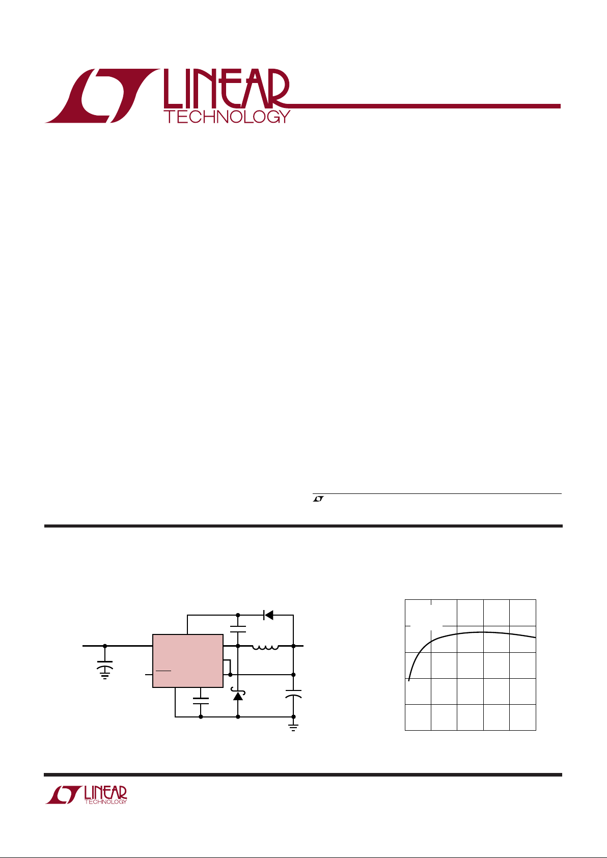
5V Buck Converter
LOAD CURRENT (A)
0
EFFICIENCY (%)
100
90
80
70
60
50
1.00
1375/76 TA02
0.25
0.50
0.75
1.25
V
OUT
= 5V
V
IN
= 10V
L = 10µH
Efficiency vs Load Current
BOOST
LT1376-5
V
IN
OUTPUT**
5V, 1.25A
* RIPPLE CURRENT ≥ I
OUT
/2
** INCREASE L1 TO 10µH FOR LOAD CURRENTS ABOVE 0.6A AND TO 20µH ABOVE 1A
†
FOR INPUT VOLTAGE BELOW 7.5V, SOME RESTRICTIONS MAY APPLY.
SEE APPLICATIONS INFORMATION.
INPUT
6V
†
TO 25V
1375/76 TA01
C2
0.1µF
C
C
3.3nF
D2
1N5818
C1
100µF, 10V
SOLID
TANTALUM
C3*
10µF TO
50µF
D2
1N914
L1**
5µH
V
SW
FB
BIAS
GND
V
C
DEFAULT
= ON
SHDN
+
+
FEATURES
APPLICATIO S
U
DESCRIPTIO
U
TYPICAL APPLICATIO
U
Page 2
2
LT1375/LT1376
ABSOLUTE MAXIMUM RATINGS
W
WW
U
Input Voltage
LT1375/LT1376.................................................. 25V
LT1375HV/LT1376HV ........................................ 30V
BOOST Pin Voltage
LT1375/LT1376.................................................. 35V
LT1375HV/LT1376HV ........................................ 40V
SHDN Pin Voltage..................................................... 7V
BIAS Pin Voltage ...................................................... 7V
FB Pin Voltage (Adjustable Part)............................ 3.5V
FB Pin Current (Adjustable Part)............................ 1mA
Sense Voltage (Fixed 5V Part) .................................. 7V
SYNC Pin Voltage ..................................................... 7V
Operating Ambient Temperature Range
LT1375C/LT1376C ................................. 0°C to 70°C
LT1375I/LT1376I............................... –40°C to 85°C
Operating Junction Temperature Range
LT1375C/LT1376C ............................... 0°C to 125° C
LT1375I/LT1376I............................. –40°C to 125°C
Storage Temperature Range................ –65° C to 150°C
Lead Temperature (Soldering, 10 sec)................. 300°C
(Note 1)
PACKAGE/ORDER INFORMATION
W
UU
TOP VIEW
S PACKAGE
16-LEAD PLASTIC NARROW SO
1
2
3
4
5
6
7
8
16
15
14
13
12
11
10
9
GND
NC
BOOST
V
IN
V
SW
BIAS
NC
GND
GND
NC
V
C
FB/SENSE
GND
SHDN
NC
GND
ORDER PART NUMBER
θJA =50°C/W WITH FUSED CORNER PINS
CONNECTED TO GROUND PLANE OR LARGE
LANDS
1
2
3
4
8
7
6
5
TOP VIEW
BOOST
V
IN
V
SW
BIAS
N8 PACKAGE
8-LEAD PDIP
S8 PACKAGE
8-LEAD PLASTIC SO
V
C
FB/SENSE
GND
SHDN
θJA = 100°C/W (N8)
θ
JA
= 120°C/W TO 150°C/W DEPENDING ON
PC BOARD LAYOUT (S8)
1
2
3
4
8
7
6
5
TOP VIEW
V
C
FB/SENSE
GND
SYNC
N8 PACKAGE
8-LEAD PDIP
S8 PACKAGE
8-LEAD PLASTIC SO
BOOST
V
IN
V
SW
SHDN
θJA = 100°C/W (N8)
θ
JA
= 120°C/W TO 150°C/W DEPENDING ON
PC BOARD LAYOUT (S8)
LT1375CN8
LT1375CN8-5
LT1375CS8
LT1375CS8-5
LT1375HVCS8
ORDER PART NUMBER
ORDER PART NUMBER
LT1375IN8
LT1375IN8-5
LT1375IS8
LT1375IS8-5
LT1375HVIS8
LT1376CN8
LT1376CN8-5
LT1376CS8
LT1376CS8-5
LT1376HVCS8
LT1376IN8
LT1376IN8-5
LT1376IS8
LT1376IS8-5
LT1376HVIS8
S8 PART MARKING S8 PART MARKING
1375I
1375I5
375HVI
1375
13755
1375HV
1376
13765
1376HV
1376I
1376I5
376HVI
LT1376CS
LT1376IS
LT1376HVCS
LT1376HVIS
Consult factory for Military grade parts.
Page 3
3
LT1375/LT1376
ELECTRICAL CHARACTERISTICS
The ● denotes specifications which apply over the full operating
temperature range, otherwise specifications are at TA = 25°C. TJ = 25°C, VIN = 15V, VC = 1.5V, boost open, switch open,
unless otherwise noted.
PARAMETER CONDITIONS MIN TYP MAX UNITS
Reference Voltage (Adjustable) 2.39 2.42 2.45 V
All Conditions
● 2.36 2.48 V
Sense Voltage (Fixed 5V) 4.94 5.0 5.06 V
All Conditions
● 4.90 5.10 V
Sense Pin Resistance 71014 kΩ
Reference Voltage Line Regulation 5V ≤ VIN ≤ 25V 0.01 0.03 %/V
5V ≤ V
IN
≤ 30V (LT1375HV/LT1376HV) 0.01 0.03 %/V
Feedback Input Bias Current ● 0.5 1.5 µA
Error Amplifier Voltage Gain V
SHDN
= 1V (Notes 2, 8) 200 400
Error Amplifier Transconductance V
SHDN
= 1V, ∆I (VC) = ±10µA (Note 8) 1500 2000 2700 µMho
● 1100 3000 µMho
VC Pin to Switch Current Transconductance 2A/V
Error Amplifier Source Current V
SHDN
= 1V, VFB = 2.1V or V
SENSE
= 4.4V ● 150 225 320 µA
Error Amplifier Sink Current V
SHDN
= 1V, VFB = 2.7V or V
SENSE
= 5.6V 2 mA
VC Pin Switching Threshold Duty Cycle = 0 0.9 V
VC Pin High Clamp V
SHDN
= 1V 2.1 V
Switch Current Limit VC Open, VFB = 2.1V or V
SENSE
= 4.4V,
V
BOOST
= VIN + 5V DC ≤ 50% ● 1.50 2 3 A
DC = 80%
● 1.35 3 A
Switch On Resistance (Note 6) ISW = 1.5A, V
BOOST
= VIN + 5V 0.3 0.4 Ω
● 0.5 Ω
Maximum Switch Duty Cycle VFB = 2.1V or V
SENSE
= 4.4V 90 93 %
–40°C ≤ T
J
≤ 125°C8693 %
T
J
= 150°C8593 %
Switch Frequency VC Set to Give 50% Duty Cycle 460 500 540 kHz
–25°C ≤ T
J
≤ 125°C 440 560 kHz
T
J
≤ –25°C 440 570 kHz
Switch Frequency Line Regulation 5V ≤ VIN ≤ 25V ● 0.05 0.15 %/V
5V ≤ V
IN
≤ 30V (LT1375HV/LT1376HV) ● 0.05 0.15 %/V
Frequency Shifting Threshold on FB Pin ∆f = 10kHz ● 0.8 1.0 1.3 V
Minimum Input Voltage (Note 3) ● 5.0 5.5 V
Minimum Boost Voltage (Note 4) ISW ≤ 1.5A ● 3 3.5 V
Boost Current (Note 5) V
BOOST
= VIN + 5V ISW = 500mA ● 12 22 mA
I
SW
= 1.5A ● 25 35 mA
Input Supply Current (Note 6) V
BIAS
= 5V ● 0.9 1.4 mA
Output Supply Current (Note 6) V
BIAS
= 5V ● 3.2 4.0 mA
Shutdown Supply Current V
SHDN
= 0V, VIN ≤ 25V, VSW = 0V, VC Open 15 50 µA
● 75 µA
V
SHDN
= 0V, VIN ≤ 30V, VSW = 0V, VC Open
(LT1375HV/LT1376HV) 20 75 µA
● 100 µA
Lockout Threshold VC Open ● 2.3 2.38 2.46 V
Page 4
4
LT1375/LT1376
Kool Mµ is a registered trademark of Magnetics, Inc.
ELECTRICAL CHARACTERISTICS
Note 1: Absolute Maximum Ratings are those values beyond which the life
of a device may be impaired.
Note 2: Gain is measured with a VC swing equal to 200mV above the low
clamp level to 200mV below the upper clamp level.
Note 3: Minimum input voltage is not measured directly, but is guaranteed
by other tests. It is defined as the voltage where internal bias lines are still
regulated so that the reference voltage and oscillator frequency remain
constant. Actual minimum input voltage to maintain a regulated output will
depend on output voltage and load current. See Applications Information.
Note 4: This is the minimum voltage across the boost capacitor needed to
guarantee full saturation of the internal power switch.
Note 5: Boost current is the current flowing into the BOOST pin with the
pin held 5V above input voltage. It flows only during switch-on time.
Note 6: Input supply current is the bias current drawn by the input pin
when the BIAS pin is held at 5V with switching disabled. Output supply
current is the current drawn by the BIAS pin when the bias pin is held at
5V. Total input referred supply current is calculated by summing input
supply current (I
SI
) with a fraction of output supply current (ISO):
I
TOT
= ISI + (ISO)(V
OUT/VIN
)(1.15)
With V
IN
= 15V, V
OUT
= 5V, ISI = 0.9mA, ISO = 3.6mA, I
TOT
= 2.28mA.
For the LT1375, quiescent current is equal to:
I
TOT
= ISI + ISO(1.15)
because the BIAS pin is internally connected to V
IN
.
Note 7: Switch-on resistance is calculated by dividing V
IN
to VSW voltage
by the forced current (1.5A). See Typical Performance Characteristics for
the graph of switch voltage at other currents.
Note 8: Transconductance and voltage gain refer to the internal amplifier
exclusive of the voltage divider. To calculate gain and transconductance
refer to sense pin on fixed voltage parts. Divide values shown by the ratio
V
OUT
/2.42.
The ● denotes specifications which apply over the full operating
temperature range, otherwise specifications are at TA = 25°C. TJ = 25°C, VIN = 15V, VC = 1.5V, boost open, switch open,
unless otherwise noted.
PARAMETER CONDITIONS MIN TYP MAX UNITS
Shutdown Thresholds VC Open Device Shutting Down ● 0.15 0.37 0.60 V
Device Starting Up
● 0.25 0.45 0.60 V
VC Open LT1375HV/LT1376HV Device Shutting Down ● 0.15 0.37 0.70 V
LT1375HV/LT1376HV Device Starting Up
● 0.25 0.45 0.70 V
Minimum Synchronizing Amplitude (LT1375 Only) VIN = 5V ● 1.5 2.2 V
Synchronizing Range (LT1375 Only) 580 900 kHz
SYNC Pin Input Resistance 40 kΩ
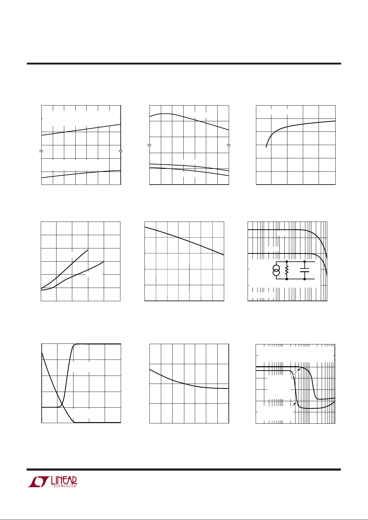
INDUCTANCE (µH)
05
CORE LOSS (W)
CORE LOSS (% OF 5W LOAD)
1.0
0.1
0.01
0.001
10 15 20
20
12
8
4
2
1.2
0.8
0.4
0.2
0.12
0.08
0.04
0.02
25
1375/76 G01
TYPE 52
POWDERED IRON
Kool Mµ
®
PERMALLOY
µ = 125
V
OUT
= 5V, VIN = 10V, I
OUT
= 1A
CORE LOSS IS
INDEPENDENT OF LOAD
CURRENT UNTIL LOAD CURRENT FALLS
LOW ENOUGH FOR CIRCUIT TO GO INTO
DISCONTINUOUS MODE
Inductor Core Loss
TYPICAL PERFORMANCE CHAR ACTERISTICS
UW
DUTY CYCLE (%)
0
SWITCH PEAK CURRENT (A)
2.5
2.0
1.5
1.0
0.5
0
80
1375/76 G08
20
40
60
100
TYPICAL
GUARANTEED MINIMUM
Switch Peak Current Limit
JUNCTION TEMPERATURE (°C)
–50
2.44
2.43
2.42
2.41
2.40
100
1375/76 G09
–25 0 25 50 75 125
FEEDBACK VOLTAGE (V)
CURRENT (µA)
2.0
1.5
1.0
0.5
0
VOLTAGE
CURRENT
Feedback Pin Voltage and Current
Page 5
5
LT1375/LT1376
TYPICAL PERFORMANCE CHAR ACTERISTICS
UW
TEMPERATURE (°C)
–50
500
400
300
200
8
4
0
25 75
1375/76 G04
–25 0
50 100 125
CURRENT (µA)
CURRENT REQUIRED TO FORCE SHUTDOWN
(FLOWS OUT OF PIN). AFTER SHUTDOWN,
CURRENT DROPS TO A FEW µA
AT 2.38V STANDBY THRESHOLD
(CURRENT FLOWS OUT OF PIN)
Shutdown Pin Bias Current
JUNCTION TEMPERATURE (°C)
–50
TRANSCONDUCTANCE (µMho)
2500
2000
1500
1000
500
0
0
50
75
1375/76 G02
–25
25
100
125
Error Amplifier Transconductance
FREQUENCY (Hz)
GAIN (µMho)
PHASE (DEG)
3000
2500
2000
1500
1000
500
200
150
100
50
0
–50
100 10k 100k 10M
1375/76 G03
1k 1M
GAIN
PHASE
ERROR AMPLIFIER EQUIVALENT CIRCUIT
R
OUT
200k
C
OUT
12pF
V
C
R
LOAD
= 50Ω
V
FB
2 • 10
–3
)(
Error Amplifier Transconductance
Frequency Foldback
LOAD CURRENT (mA)
0
INPUT VOLTAGE (V)
8.5
8.0
7.5
7.0
6.5
6.0
5.5
5.0
10 100 1000
1375/76 G12
MINIMUM INPUT VOLTAGE CAN BE
REDUCED BY ADDING A SMALL EXTERNAL
PNP. SEE APPLICATIONS INFORMATION
MINIMUM
VOLTAGE TO
START WITH
STANDARD
CIRCUIT
MINIMUM VOLTAGE
TO RUN WITH
STANDARD CIRCUIT
LT1376 Minimum Input Voltage
with 5V Output
Shutdown Supply Current
INPUT VOLTAGE (V)
0
INPUT SUPPLY CURRENT (µA)
30
25
20
15
10
5
0
5101520
1375/76 G06
25
V
SHUTDOWN
= 0V
JUNCTION TEMPERATURE (°C)
–50
2.40
2.36
2.32
0.8
0.4
0
25 75
1375/76 G05
–25 0
50 100 125
SHUTDOWN PIN VOLTAGE (V)
STANDBY
START-UP
SHUTDOWN
Standby and Shutdown Thresholds
Shutdown Supply Current
SHUTDOWN VOLTAGE (V)
0
INPUT SUPPLY CURRENT (µA)
150
125
100
75
50
25
0
0.1 0.2 0.3 0.4
1375/76 G07
0.5
VIN = 25V
VIN = 10V
FEEDBACK PIN VOLTAGE (V)
0
SWITCHING FREQUENCY (kHz) OR CURRENT (µA)
500
400
300
200
100
0
2.0
1375/76 G10
0.5
1.0
1.5
2.5
SWITCHING
FREQUENCY
FEEDBACK PIN
CURRENT
Switching Frequency
JUNCTION TEMPERATURE (°C)
–50
600
550
500
450
400
100
1375/76 G11
–25 0 25 50 75 125
FREQUENCY (kHz)
Page 6
6
LT1375/LT1376
TYPICAL PERFORMANCE CHARACTERISTICS
U
W
INPUT VOLTAGE (V)
0
CURRENT (A)
1.50
1.25
1.00
0.75
0.50
0.25
0
5101520
1375/76 G13
25
L = 20µH
L = 10µH
L = 5µH
V
OUT
= 10V
INPUT VOLTAGE (V)
0
CURRENT (A)
1.50
1.25
1.00
0.75
0.50
0.25
0
5101520
1375/76 G14
25
L = 20µH
L = 10µH
L = 5µH
V
OUT
= 3.3V
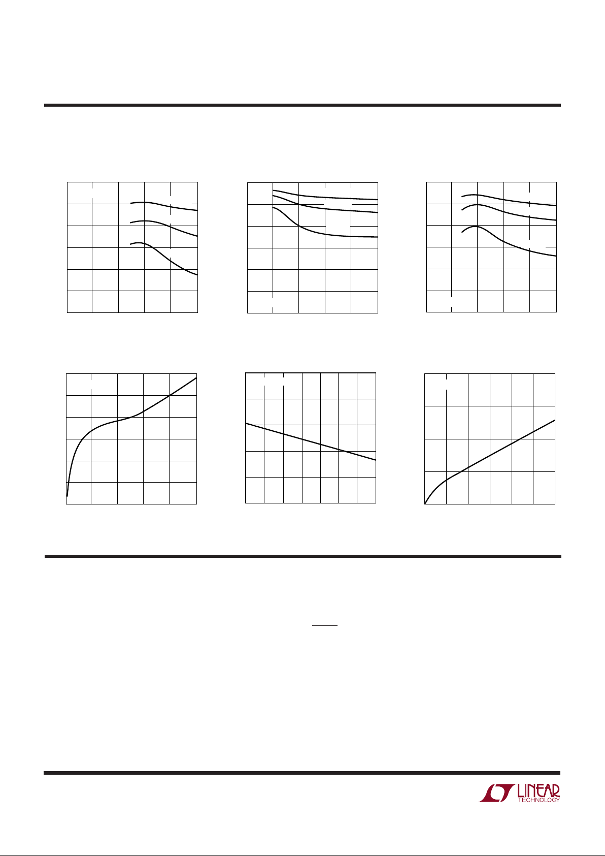
Maximum Load Current
at V
OUT
= 10V
Maximum Load Current
at V
OUT
= 3.3V
Maximum Load Current
at V
OUT
= 5V
INPUT VOLTAGE (V)
0
CURRENT (A)
1.50
1.25
1.00
0.75
0.50
0.25
0
5101520
1375/76 G15
25
L = 20µH
L = 10µH
L = 5µH
V
OUT
= 5V
PIN FUNCTIONS
UUU
BOOST: The BOOST pin is used to provide a drive voltage,
higher than the input voltage, to the internal bipolar NPN
power switch. Without this added voltage, the typical
switch voltage loss would be about 1.5V. The additional
boost voltage allows the switch to saturate and voltage
loss approximates that of a 0.3Ω FET structure, but with
much smaller die area. Efficiency improves from 75% for
conventional bipolar designs to > 87% for these new parts.
VSW: The switch pin is the emitter of the on-chip power
NPN switch. It is driven up to the input pin voltage during
switch on time. Inductor current drives the switch pin
negative during switch off time. Negative voltage is clamped
with the external catch diode. Maximum negative switch
voltage allowed is –0.8V.
SHDN: The shutdown pin is used to turn off the regulator
and to reduce input drain current to a few microamperes.
Actually, this pin has two separate thresholds, one at
2.38V to disable switching, and a second at 0.4V to force
complete micropower shutdown. The 2.38V threshold
functions as an accurate undervoltage lockout (UVLO).
This is sometimes used to prevent the regulator from
operating until the input voltage has reached a predetermined level.
SWITCH CURRENT (A)
0
BOOST PIN CURRENT (mA)
12
10
8
6
4
2
0
0.25 0.50 0.75 1.00
1375/76 G16
1.25
TJ = 25°C
BOOST Pin Current
VC Pin Shutdown Threshold
SWITCH CURRENT (A)
0
SWITCH VOLTAGE (V)
0.8
0.6
0.4
0.2
0
0.25 0.50 0.75 1.00
1375/76 G18
1.25 1.50
TJ = 25°C
Switch Voltage Drop
JUNCTION TEMPERATURE (°C)
–50
1.4
1.2
1.0
0.8
0.6
0.4
100
1375/76 G11
–25 0 25 50 75 125
THRESHOLD VOLTAGE (V)
SHUTDOWN
Page 7
7
LT1375/LT1376
PIN FUNCTIONS
UUU
BIAS (LT1376 Only): The BIAS pin is used to improve
efficiency when operating at higher input voltages and
light load current. Connecting this pin to the regulated
output voltage forces most of the internal circuitry to draw
its operating current from the output voltage rather than
the input supply. This is a much more efficient way of
doing business if the input voltage is much higher than the
output.
Minimum output voltage setting for this mode of
operation is 3.3V
. Efficiency improvement at VIN = 20V,
V
OUT
= 5V, and I
OUT
= 25mA is over 10%.
SYNC (LT1375 Only): The SYNC pin is used to synchronize the internal oscillator to an external signal. It is directly
logic compatible and can be driven with any signal between 10% and 90% duty cycle. The synchronizing range
is equal to
initial
operating frequency, up to 900kHz. See
Synchronizing section in Applications Information for
details.
FB/SENSE: The feedback pin is used to set output voltage,
using an external voltage divider that generates 2.42V at
the pin with the desired output voltage. The fixed voltage
(-5) parts have the divider included on the chip, and the FB
pin is used as a SENSE pin, connected directly to the 5V
output. Two additional functions are performed by the FB
pin. When the pin voltage drops below 1.7V, switch
current limit is reduced. Below 1V, switching frequency is
also reduced. See Feedback Pin Function section in Applications Information for details.
VC: The VC pin is the output of the error amplifier and the
input of the peak switch current comparator. It is normally
used for frequency compensation, but can do double duty
as a current clamp or control loop override. This pin sits
at about 1V for very light loads and 2V at maximum load.
It can be driven to ground to shut off the regulator, but if
driven high, current must be limited to 4mA.
GND: The GND pin connection needs consideration for
two reasons. First, it acts as the reference for the regulated
output, so load regulation will suffer if the “ground” end of
the load is not at the same voltage as the GND pin of the
IC. This condition will occur when load current or other
currents flow through metal paths between the GND pin
and the load ground point. Keep the ground path short
between the GND pin and the load, and use a ground plane
when possible. The second consideration is EMI caused
by GND pin current spikes. Internal capacitance between
the VSW pin and the GND pin creates very narrow (<10ns)
current spikes in the GND pin. If the GND pin is connected
to system ground with a long metal trace, this trace may
radiate excess EMI. Keep the path between the input
bypass and the GND pin short.
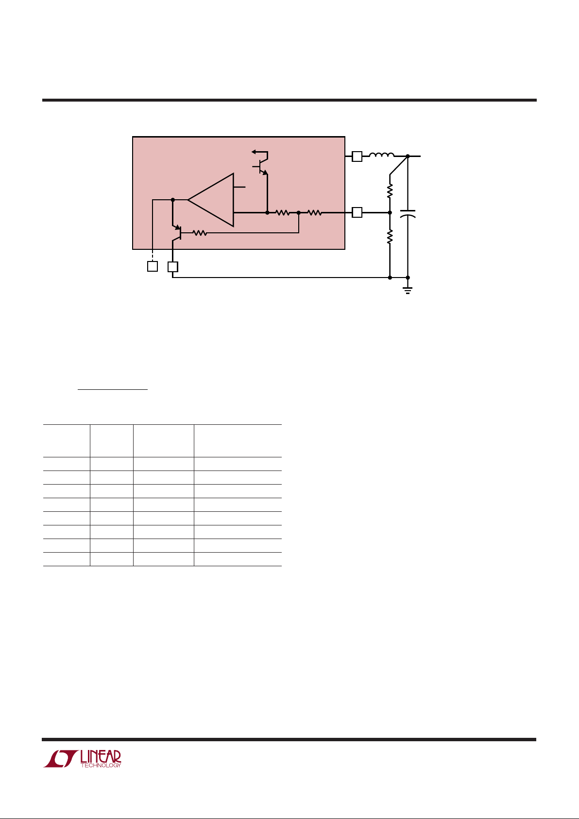
BLOCK DIAGRAM
W
The LT1376 is a constant frequency, current mode buck
converter. This means that there is an internal clock and
two feedback loops that control the duty cycle of the power
switch. In addition to the normal error amplifier, there is a
current sense amplifier that monitors switch current on a
cycle-by-cycle basis. A switch cycle starts with an oscillator pulse which sets the RS flip-flop to turn the switch on.
When switch current reaches a level set by the inverting
input of the comparator, the flip-flop is reset and the
switch turns off. Output voltage control is obtained by
using the output of the error amplifier to set the switch
current trip point. This technique means that the error
amplifier commands current to be delivered to the output
rather than voltage. A voltage fed system will have low
phase shift up to the resonant frequency of the inductor
and output capacitor, then an abrupt 180° shift will occur.
The current fed system will have 90° phase shift at a much
lower frequency, but will not have the additional 90° shift
until well beyond the LC resonant frequency. This makes
it much easier to frequency compensate the feedback loop
and also gives much quicker transient response.
Most of the circuitry of the LT1376 operates from an
internal 2.9V bias line. The bias regulator normally draws
power from the regulator input pin, but if the BIAS pin is
connected to an external voltage higher than 3V, bias
power will be drawn from the external source (typically the
regulated output voltage). This will improve efficiency if
the BIAS pin voltage is lower than regulator input voltage.
Page 8
8
LT1375/LT1376
High switch efficiency is attained by using the BOOST pin
to provide a voltage to the switch driver which is higher
than the input voltage, allowing switch to be saturated.
This boosted voltage is generated with an external capaci-
BLOCK DIAGRAM
W
tor and diode. Two comparators are connected to the
shutdown pin. One has a 2.38V threshold for undervoltage
lockout and the second has a 0.4V threshold for complete
shutdown.
–
+
–
+
–
+
–
+
Σ
INPUT
2.9V BIAS
REGULATOR
500kHz
OSCILLATOR
FREQUENCY
SHIFT CIRCUIT
V
SW
FB
V
C
GND
1375/76 BD
SLOPE COMP
0.1Ω
BIAS
INTERNAL
V
CC
CURRENT
SENSE
AMPLIFIER
VOLTAGE GAIN = 10
SYNC
SHUTDOWN
COMPARATOR
CURRENT
COMPARATOR
ERROR
AMPLIFIER
g
m
= 2000µMho
FOLDBACK
CURRENT
LIMIT
CLAMP
BOOST
R
S
FLIP-FLOP
DRIVER
CIRCUITRY
S
R
0.9V
LOCKOUT
COMPARATOR
0.4V
3.5µA
Q2
Q1
POWER
SWITCH
2.38V
2.42V
–
+
SHDN
Figure 1. Block Diagram
APPLICATIONS INFORMATION
WUU
U
FEEDBACK PIN FUNCTIONS
The feedback (FB) pin on the LT1376 is used to set output
voltage and also to provide several overload protection
features. The first part of this section deals with selecting
resistors to set output voltage and the remaining part talks
about foldback frequency and current limiting created by
the FB pin. Please read both parts before committing to a
final design. The fixed 5V LT1376-5 has internal divider
resistors and the FB pin is renamed SENSE, connected
directly to the output.
The suggested value for the output divider resistor (see
Figure 2) from FB to ground (R2) is 5k or less, and a
formula for R1 is shown below. The output voltage error
caused by ignoring the input bias current on the FB pin is
less than 0.25% with R2 = 5k. A table of standard 1%
values is shown in Table 1 for common output voltages.
Page 9
9
LT1375/LT1376
APPLICATIONS INFORMATION
WUU
U
–
+
2.4V
V
SW
V
C
GND
1375/76 F02
TO FREQUENCY
SHIFTING
R3
1k
R4
1k
R1
R2
5k
OUTPUT
5V
R5
5k
ERROR
AMPLIFIER
FB
1.6V
Q1
LT1375/LT1376
Q2
+
Figure 2. Frequency and Current Limit Foldback
Please read the following if divider resistors are increased
above the suggested values.
R
RV
OUT
1
2242
242
=
−
()
.
.
Table 1
OUTPUT R1 % ERROR AT OUTPUT
VOLTAGE R2 (NEAREST 1%) DUE TO DISCREET 1%
(V) (k
Ω
)(k
Ω
) RESISTOR STEPS
3 4.99 1.21 +0.23
3.3 4.99 1.82 +0.08
5 4.99 5.36 +0.39
6 4.99 7.32 –0.5
8 4.99 11.5 –0.04
10 4.99 15.8 +0.83
12 4.99 19.6 –0.62
15 4.99 26.1 +0.52
More Than Just Voltage Feedback
The feedback (FB) pin is used for more than just output
voltage sensing. It also reduces switching frequency and
current limit when output voltage is very low (see the
Frequency Foldback graph in Typical Performance Characteristics). This is done to control power dissipation in
both the IC and in the external diode and inductor during
short-circuit conditions. A shorted output requires the
switching regulator to operate at very low duty cycles, and
the average current through the diode and inductor is
equal to the short-circuit current limit of the switch (typically 2A for the LT1376, folding back to less than 1A).
Minimum switch on time limitations would prevent the
switcher from attaining a sufficiently low duty cycle if
switching frequency were maintained at 500kHz, so frequency is reduced by about 5:1 when the feedback pin
voltage drops below 1V (see Frequency Foldback graph).
This does not affect operation with normal load conditions; one simply sees a gear shift in switching frequency
during start-up as the output voltage rises.
In addition to lower switching frequency, the LT1376 also
operates at lower switch current limit when the feedback
pin voltage drops below 1.7V. Q2 in Figure 2 performs this
function by clamping the VC pin to a voltage less than its
normal 2.3V upper clamp level. This
foldback current limit
greatly reduces power dissipation in the IC, diode and
inductor during short-circuit conditions. Again, it is nearly
transparent to the user under normal load conditions. The
only loads which may be affected are current source loads
which maintain full load current with output voltage less
than 50% of final value. In these rare situations the
Feedback pin can be clamped above 1.5V with an external
diode to defeat foldback current limit.
Caution:
clamping
the feedback pin means that frequency shifting will also be
defeated, so a combination of high input voltage and dead
shorted output may cause the LT1376 to lose control of
current limit.
The internal circuitry which forces reduced switching
frequency also causes current to flow out of the feedback
Page 10

10
LT1375/LT1376
APPLICATIONS INFORMATION
WUU
U
pin when output voltage is low. The equivalent circuitry is
shown in Figure 2. Q1 is completely off during normal
operation. If the FB pin falls below 1V, Q1 begins to
conduct current and reduces frequency at the rate of
approximately 5kHz/µA. To ensure adequate frequency
foldback (under worst-case short-circuit conditions), the
external divider Thevinin resistance must be low enough
to pull 150µ A out of the FB pin with 0.6V on the pin (R
DIV
≤ 4k).
The net result is that reductions in frequency and
current limit are affected by output voltage divider impedance. Although divider impedance is not critical, caution
should be used if resistors are increased beyond the
suggested values and short-circuit conditions will occur
with high input voltage
. High frequency pickup will increase and the protection accorded by frequency and
current foldback will decrease.
MAXIMUM OUTPUT LOAD CURRENT
Maximum load current for a buck converter is limited by
the maximum switch current rating (IP) of the LT1376.
This current rating is 1.5A up to 50% duty cycle (DC),
decreasing to 1.35A at 80% duty cycle. This is shown
graphically in Typical Performance Characteristics and as
shown in the formula below:
IP = 1.5A for DC ≤ 50%
IP = 1.65A – 0.15 (DC) – 0.26 (DC)2 for 50% < DC < 90%
DC = Duty cycle = V
OUT/VIN
Example: with V
OUT
= 5V, VIN = 8V; DC = 5/8 = 0.625, and;
I
SW(MAX)
= 1.64 – 0.15 (0.625) – 0.26 (0.625)2 = 1.44A
Current rating decreases with duty cycle because the
LT1376 has internal slope compensation to prevent current mode subharmonic switching. For more details, read
Application Note 19. The LT1376 is a little unusual in this
regard because it has nonlinear slope compensation which
gives better compensation with less reduction in current
limit.
Maximum load current would be equal to maximum
switch current
for an infinitely large inductor
, but with
finite inductor size, maximum load current is reduced by
one-half peak-to-peak inductor current. The following
formula assumes continuous mode operation, implying
that the term on the right is less than one-half of IP.
I
OUT(MAX)
=
Continuous Mode
For the conditions above and L = 10µH,
I
A
OUT MAX
(
)
−
=−
()
−
()
()
=−=
144
58 5
2 10 500 10 8
144 019 125
53
.
•
...
At VIN = 15V, duty cycle is 33%, so IP is just equal to a fixed
1.5A, and I
OUT(MAX)
is equal to:
15
515 5
2 10 500 10 15
15 033 117
53
.
•
.. .−
()
−
()
()
=− =−A
Note that there is less load current available at the higher
input voltage because inductor ripple current increases.
This is not always the case. Certain combinations of
inductor value and input voltage range may yield lower
available load current at the lowest input voltage due to
reduced peak switch current at high duty cycles. If load
current is close to the maximum available, please check
maximum available current at both input voltage extremes. To calculate actual peak switch current with a
given set of conditions, use:
II
VVV
LfV
SW PEAK OUT
OUT IN OUT
IN
(
)
=+
−
()
()()( )
2
For lighter loads where discontinuous operation can be
used, maximum load current is equal to:
I
OUT(MAX)
=
Discontinuous mode
I
P
−
()
−
()
()()( )
VVV
LfV
OUT IN OUT
IN
2
IfLV
VVV
P OUT
OUT IN OUT
()()()( )
()
−
()
2
2
Page 11

11
LT1375/LT1376
APPLICATIONS INFORMATION
WUU
U
must withstand continuous fault conditions. If maximum load current is 0.5A, for instance, a 0.5A inductor
may not survive a continuous 1.5A overload condition.
Dead shorts will actually be more gentle on the inductor because the LT1376 has foldback current limiting.
2. Calculate peak inductor current at full load current to
ensure that the inductor will not saturate. Peak current
can be significantly higher than output current, especially with smaller inductors and lighter loads, so don’t
omit this step. Powdered iron cores are forgiving
because they saturate softly, whereas ferrite cores
saturate abruptly. Other core materials fall in between
somewhere. The following formula assumes continuous mode of operation, but it errs only slightly on the
high side for discontinuous mode, so it can be used for
all conditions.
II
VVV
fLV
PEAK OUT
OUT IN OUT
IN
=+
−
()
()()( )
2
VIN = Maximum input voltage
f = Switching frequency, 500kHz
3. Decide if the design can tolerate an “open” core geometry like a rod or barrel, which have high magnetic field
radiation, or whether it needs a closed core like a toroid
to prevent EMI problems. One would not want an open
core next to a magnetic storage media, for instance!
This is a tough decision because the rods or barrels are
temptingly cheap and small and there are no helpful
guidelines to calculate when the magnetic field radiation will be a problem.
4. Start shopping for an inductor (see representative
surface mount units in Table 2) which meets the requirements of core shape, peak current (to avoid saturation), average current (to limit heating), and fault
current (if the inductor gets too hot, wire insulation will
melt and cause turn-to-turn shorts). Keep in mind that
all good things like high efficiency, low profile, and high
temperature operation will increase cost, sometimes
dramatically. Get a quote on the cheapest unit first to
calibrate yourself on price, then ask for what you really
want.
Example: with L = 2µH, V
OUT
= 5V, and V
IN(MAX
) = 15V,
ImA
OUT MAX
(
)
−
=
()
()
()
−
()
=
15 500 10 2 10 15
2 5 15 5
338
2
36
.••
The main reason for using such a tiny inductor is that it is
physically very small, but keep in mind that peak-to-peak
inductor current will be very high. This will increase output
ripple voltage. If the output capacitor has to be made larger
to reduce ripple voltage, the overall circuit could actually
wind up larger.
CHOOSING THE INDUCTOR AND OUTPUT CAPACITOR
For most applications the output inductor will fall in the
range of 3µ H to 20µ H. Lower values are chosen to reduce
physical size of the inductor. Higher values allow more
output current because they reduce peak current seen by
the LT1376 switch, which has a 1.5A limit. Higher values
also reduce output ripple voltage, and reduce core loss.
Graphs in the Typical Performance Characteristics section
show maximum output load current versus inductor size
and input voltage. A second graph shows core loss versus
inductor size for various core materials.
When choosing an inductor you might have to consider
maximum load current, core and copper losses, allowable
component height, output voltage ripple, EMI, fault current in the inductor, saturation, and of course, cost. The
following procedure is suggested as a way of handling
these somewhat complicated and conflicting requirements.
1. Choose a value in microhenries from the graphs of
maximum load current and core loss. Choosing a small
inductor with lighter loads may result in discontinuous
mode of operation, but the LT1376 is designed to work
well in either mode. Keep in mind that lower core loss
means higher cost, at least for closed core geometries
like toroids. The core loss graphs show both absolute
loss and percent loss for a 5W output, so actual percent
losses must be calculated for each situation.
Assume that the average inductor current is equal to
load current and decide whether or not the inductor
Page 12

12
LT1375/LT1376
APPLICATIONS INFORMATION
WUU
U
5. After making an initial choice, consider the secondary
things like output voltage ripple, second sourcing, etc.
Use the experts in the Linear Technology’s applications department if you feel uncertain about the final
choice. They have experience with a wide range of
inductor types and can tell you about the latest developments in low profile, surface mounting, etc.
Table 2
SERIES CORE
VENDOR/ VALUE DC CORE RESIS- MATER- HEIGHT
PART NO. (
µ
H) (Amps) TYPE TANCE(Ω) IAL (mm)
Coiltronics
CTX5-1 5 2.3 Tor 0.027 KMµ 4.2
CTX10-1 10 1.9 Tor 0.039 KMµ 4.2
CTX20-1 20 1.0 Tor 0.137 KMµ 4.2
CTX15-2 15 1.8 Tor 0.058 KMµ 6.0
CTX20-3 20 1.5 Tor 0.093 KMµ 4.7
CTX20-4 20 2.2 Tor 0.059 KMµ 6.4
CTX5-1P 5 1.8 Tor 0.021 52 4.2
CTX10-1P 10 1.6 Tor 0.030 52 4.2
CTX15-1P 15 1.2 Tor 0.046 52 4.2
CTX20-1P 20 1.0 Tor 0.081 52 4.2
CTX20-2P 20 1.3 Tor 0.052 52 6.0
CTX20-4P 20 1.8 Tor 0.039 52 6.35
Sumida
CDRH64 10 1.7 SC 0.084 Fer 4.5
CDRH74 22 1.2 SC 0.077 Fer 4.5
CDRH73 10 1.7 SC 0.055 Fer 3.4
CDRH73 22 1.1 SC 0.15 Fer 3.4
CD73 10 1.4 Open 0.062 Fer 3.5
CD73 18 1.1 Open 0.085 Fer 3.5
CD104 10 2.4 Open 0.041 Fer 4.0
CD104 18 1.7 Open 0.062 Fer 4.0
Gowanda
SM20-102K 10 1.3 Open 0.038 Fer 7.0
SM20-152K 15 1.3 Open 0.049 Fer 7.0
SM20-222K 22 1.3 Open 0.059 Fer 7.0
Dale
IHSM-4825 10 3.1 Open 0.071 Fer 5.6
IHSM-4825 22 1.7 Open 0.152 Fer 5.6
IHSM-5832 10 4.3 Open 0.053 Fer 7.1
IHSM-5832 22 2.8 Open 0.12 Fer 7.1
IHSM-7832 22 3.8 Open 0.054 Fer 7.1
Tor = Toroid
SC = Semi-closed geometry
Fer = Ferrite core material
52 = Type 52 powdered iron core material
KMµ = Kool Mµ
Output Capacitor
The output capacitor is normally chosen by its Effective
Series Resistance (ESR), because this is what determines
output ripple voltage. At 500kHz, any polarized capacitor
is essentially resistive. To get low ESR takes
volume
, so
physically smaller capacitors have high ESR. The ESR
range for typical LT1376 applications is 0.05Ω to 0.5Ω. A
typical output capacitor is an AVX type TPS, 100µ F at 10V,
with a guaranteed ESR less than 0.1Ω. This is a “D” size
surface mount solid tantalum capacitor. TPS capacitors
are specially constructed and tested for low ESR, so they
give the lowest ESR for a given volume. The value in
microfarads is not particularly critical, and values from
22µF to greater than 500µF work well, but you cannot
cheat mother nature on ESR. If you find a tiny 22µ F solid
tantalum capacitor, it will have high ESR, and output ripple
voltage will be terrible. Table 3 shows some typical solid
tantalum surface mount capacitors.
Table 3. Surface Mount Solid Tantalum Capacitor ESR
and Ripple Current
E Case Size ESR (Max., Ω) Ripple Current (A)
AVX TPS, Sprague 593D 0.1 to 0.3 0.7 to 1.1
AVX TAJ 0.7 to 0.9 0.4
D Case Size
AVX TPS, Sprague 593D 0.1 to 0.3 0.7 to 1.1
AVX TAJ 0.9 to 2.0 0.36 to 0.24
C Case Size
AVX TPS 0.2 (typ) 0.5 (typ)
AVX TAJ 1.8 to 3.0 0.22 to 0.17
B Case Size
AVX TAJ 2.5 to 10 0.16 to 0.08
Many engineers have heard that solid tantalum capacitors
are prone to failure if they undergo high surge currents.
This is historically true, and type TPS capacitors are
specially tested for surge capability, but surge ruggedness
is not a critical issue with the
output
capacitor. Solid
tantalum capacitors fail during very high
turn-on
surges,
which do not occur at the output of regulators. High
Page 13

13
LT1375/LT1376
APPLICATIONS INFORMATION
WUU
U
discharge
surges, such as when the regulator output is
dead shorted, do not harm the capacitors.
Unlike the input capacitor, RMS ripple current in the
output capacitor is normally low enough that ripple current rating is not an issue. The current waveform is
triangular with a typical value of 200mA
RMS
. The formula
to calculate this is:
Output Capacitor Ripple Current (RMS):
I
VVV
LfV
RIPPLE RMS
OUT IN OUT
IN
(
)
=
()
−
()
()()( )
029.
Ceramic Capacitors
Higher value, lower cost ceramic capacitors are now
becoming available in smaller case sizes. These are tempting for switching regulator use because of their very low
ESR. Unfortunately, the ESR is so low that it can cause
loop stability problems. Solid tantalum capacitor’s ESR
generates a loop “zero” at 5kHz to 50kHz that is instrumental in giving acceptable loop phase margin. Ceramic capacitors remain capacitive to beyond 300kHz and usually
resonate with their ESL before ESR becomes effective.
They are appropriate for input bypassing because of their
high ripple current ratings and tolerance of turn-on surges.
For further information on ceramic and other capacitor
types please refer to Design Note 95.
OUTPUT RIPPLE VOLTAGE
Figure 3 shows a typical output ripple voltage waveform
for the LT1376. Ripple voltage is determined by the high
frequency impedance of the output capacitor, and ripple
current through the inductor. Peak-to-peak ripple current
through the inductor into the output capacitor is:
I
VVV
VLf
P
OUT IN OUT
IN
-P
=
()
−
()
()()()
For high frequency switchers, the sum of ripple current
slew rates may also be relevant and can be calculated
from:
Σ
dIdtV
L
IN
=
Peak-to-peak output ripple voltage is the sum of a
triwave
created by peak-to-peak ripple current times ESR, and a
square
wave created by parasitic inductance (ESL) and
ripple current slew rate. Capacitive reactance is assumed
to be small compared to ESR or ESL.
V I ESR ESL
dI
dt
RIPPLE
=
()( )
+
()
P-P
Σ
Example: with VIN =10V, V
OUT
= 5V, L = 10µ H, ESR = 0.1Ω,
ESL = 10nH:
IA
dI
dt
VA
mV
RIPPLE
P-P
P-P
=
()
−
()
()
=
==
=
()()
+
=+=
−
−
−
510 5
10 10 10 500 10
05
10
10 10
10
05 01 10 10 10
0 05 0 01 60
63
6
6
96
••
.
•
.. •
..
Σ
V
OUT
AT I
OUT
= 1A
V
OUT
AT I
OUT
= 50mA
INDUCTOR CURRENT
AT I
OUT
= 1A
0.5µs/DIV
1375/76 F03
Figure 3. LT1376 Ripple Voltage Waveform
INDUCTOR CURRENT
AT I
OUT
= 50mA
20mV/DIV
0.5A/DIV
CATCH DIODE
The suggested catch diode (D1) is a 1N5818 Schottky, or
its Motorola equivalent, MBR130. It is rated at 1A average
forward current and 30V reverse voltage. Typical forward
voltage is 0.42V at 1A. The diode conducts current only
during switch off time. Peak reverse voltage is equal to
Page 14

14
LT1375/LT1376
APPLICATIONS INFORMATION
WUU
U
regulator input voltage. Average forward current in normal
operation can be calculated from:
I
IVV
V
D AVG
OUT IN OUT
IN
(
)
=
−
()
This formula will not yield values higher than 1A with
maximum load current of 1.25A unless the ratio of input
to output voltage exceeds 5:1. The only reason to consider
a larger diode is the worst-case condition of a high input
voltage and
overloaded
(not shorted) output. Under shortcircuit conditions, foldback current limit will reduce diode
current to less than 1A, but if the output is overloaded and
does not fall to less than 1/3 of nominal output voltage,
foldback will not take effect. With the overloaded condition, output current will increase to a typical value of 1.8A,
determined by peak switch current limit of 2A. With
VIN = 15V, V
OUT
= 4V (5V overloaded) and I
OUT
= 1.8A:
IA
D AVG
(
)
=
−
()
=
18 15 4
15
132..
This is safe for short periods of time, but it would be
prudent to check with the diode manufacturer if continuous operation under these conditions must be tolerated.
BOOST PIN CONSIDERATIONS
For most applications, the boost components are a 0.1µ F
capacitor and a 1N914 or 1N4148 diode. The anode is
connected to the regulated output voltage and this generates a voltage across the boost capacitor nearly identical
to the regulated output. In certain applications, the anode
may instead be connected to the unregulated input voltage. This could be necessary if the regulated output
voltage is very low (< 3V) or if the input voltage is less than
6V. Efficiency is not affected by the capacitor value, but the
capacitor should have an ESR of less than 2Ω to ensure
that it can be recharged fully under the worst-case condition of minimum input voltage. Almost any type of film or
ceramic capacitor will work fine.
WARNING!
Peak voltage on the BOOST pin is the sum of
unregulated input voltage plus the voltage across the
boost capacitor. This normally means that peak BOOST
pin voltage is equal to input voltage plus output voltage,
but
when the boost diode is connected to the regulator
input, peak BOOST pin voltage is equal to twice the input
voltage. Be sure that BOOST pin voltage does not exceed
its maximum rating
.
For nearly all applications, a 0.1uF boost capacitor works
just fine, but for the curious, more details are provided
here. The size of the boost capacitor is determined by
switch drive current requirements. During switch on time,
drain current on the capacitor is approximately 10mA +
I
OUT
/75. At peak load current of 1.25A, this gives a total
drain of 27mA. Capacitor ripple voltage is equal to the
product of on time and drain current divided by capacitor
value; ∆V = tON • 27mA/C. To keep capacitor ripple voltage
to less than 0.5V (a slightly arbitrary number) at the worstcase condition of tON = 1.8µs, the capacitor needs to be
0.1µF. Boost capacitor ripple voltage is not a critical
parameter, but if the minimum voltage across the capacitor drops to less than 3V, the power switch may not
saturate fully and efficiency will drop. An
approximate
formula for absolute minimum capacitor value is:
C
mA I V V
fV V
MIN
OUT OUT IN
OUT
=
+
()()
()
−
()
10 753//
f = Switching frequency
V
OUT
= Regulated output voltage
VIN = Minimum input voltage
This formula can yield capacitor values substantially less
than 0.1µ F, but it should be used with caution since it does
not take into account secondary factors such as capacitor
series resistance, capacitance shift with temperature and
output overload.
SHUTDOWN FUNCTION AND UNDERVOLTAGE
LOCKOUT
Figure 4 shows how to add undervoltage lockout (UVLO)
to the LT1376. Typically, UVLO is used in situations where
the input supply is
current limited
, or has a relatively high
source resistance. A switching regulator draws constant
power from the source, so source current increases as
source voltage drops. This looks like a negative resistance
load to the source and can cause the source to current limit
Page 15

15
LT1375/LT1376
APPLICATIONS INFORMATION
WUU
U
–
+
–
+
2.38V
0.4V
GND
V
SW
LT1375/LT1376
INPUT
R
FB
R
HI
1375/76 F04
OUTPUT
SHDN
STANDBY
IN
TOTAL
SHUTDOWN
3.5µA
R
LO
C1
+
Figure 4. Undervoltage Lockout
or latch low under low source voltage conditions. UVLO
prevents the regulator from operating at source voltages
where these problems might occur.
Threshold voltage for lockout is about 2.38V, slightly less
than the internal 2.42V reference voltage. A 3.5µA bias
current flows
out
of the pin at threshold. This internally
generated current is used to force a default high state on
the shutdown pin if the pin is left open. When low shutdown current is not an issue, the error due to this current
can be minimized by making R
LO
10k or less. If shutdown
current is an issue, RLO can be raised to 100k, but the error
due to initial bias current and changes with temperature
should be considered.
Rk
R
RV V
VR A
LO
HI
LO IN
LO
=
()
=
−
()
−
()
10
238
238 35
to 100k 25k suggested
.
..µ
V
IN
= Minimum input voltage
Keep the connections from the resistors to the shutdown
pin short and make sure that interplane or surface capacitance to the switching nodes are minimized. If high resistor values are used, the shutdown pin should be bypassed
with a 1000pF capacitor to prevent coupling problems
from the switch node. If hysteresis is desired in the
undervoltage lockout point, a resistor RFB can be added to
the output node. Resistor values can be calculated from:
R
RV VV V
RA
RRV V
HI
LO IN OUT
FB HI OUT
=
−+
()
+
[]
−
()
=
()( )
238 1
238 235
./
..
/
∆∆
∆
µ
25k suggested for R
LO
VIN= Input voltage at which switching stops as input
voltage descends to trip level
∆V = Hysteresis in input voltage level
Example: output voltage is 5V, switching is to stop if input
voltage drops below 12V and should not restart unless
input rises back to 13.5V. ∆V is therefore 1.5V and VIN =
12V. Let RLO = 25k.
R
k
kA
k
k
Rk k
HI
FB
=
−+
()
+
[]
−
()
=
()
=
=
()
=
25 12 2 38 1 5 5 1 1 5
238 25 35
25 10 41
229
114
114 5 1 5 380
../ .
..
.
.
/.
µ
SWITCH NODE CONSIDERATIONS
For maximum efficiency, switch rise and fall times are
made as short as possible. To prevent radiation and high
frequency resonance problems, proper layout of the components connected to the switch node is essential. B field
Page 16

16
LT1375/LT1376
APPLICATIONS INFORMATION
WUU
U
(magnetic) radiation is minimized by keeping catch diode,
switch pin, and input bypass capacitor leads as short as
possible. E field radiation is kept low by minimizing the
length and area of all traces connected to the switch pin
and BOOST pin. A ground plane should always be used
under the switcher circuitry to prevent interplane coupling. A suggested layout for the critical components is
shown in Figure 5. Note that the feedback resistors and
compensation components are kept as far as possible
from the switch node. Also note that the high current
ground path of the catch diode and input capacitor are kept
very short and separate from the analog ground line.
The high speed switching current path is shown schematically in Figure 6. Minimum lead length in this path is
essential to ensure clean switching and low EMI. The path
including the switch, catch diode, and input capacitor is
the only one containing nanosecond rise and fall times. If
you follow this path on the PC layout, you will see that it is
irreducibly short. If you move the diode or input capacitor
away from the LT1376, get your resumé in order. The
other paths contain only some combination of DC and
500kHz triwave, so are much less critical.
Figure 5. Suggested Layout
INPUT
C2
C3
D2
C
C
R
C
R1
C1
1375/76 F05
D1
L1
R2
BOOST
IN
SW
BIAS
V
C
FB
GND
SHDN
SHUTDOWN
OUTPUT
MINIMIZE AREA OF
CONNECTIONS TO THE
SWITCH NODE AND
BOOST NODE
KEEP INPUT CAPACITOR
AND CATCH DIODE CLOSE
TO REGULATOR AND
TERMINATE THEM
TO SAME POINT
CONNECT OUTPUT CAPACITOR
DIRECTLY TO HEAVY GROUND
TAKE OUTPUT DIRECTLY FROM END OF OUTPUT
CAPACITOR TO AVOID PARASITIC RESISTANCE
AND INDUCTANCE (KELVIN CONNECTION)
MINIMIZE SIZE OF
FEEDBACK PIN
CONNECTIONS TO
AVOID PICKUP
TERMINATE
FEEDBACK RESISTORS
AND COMPENSATION
COMPONENTS
DIRECTLY TO SWITCHER
GROUND PIN
GROUND RING NEED
NOT BE AS SHOWN.
(NORMALLY EXISTS AS
INTERNAL PLANE)
Figure 6. High Speed Switching Path
1375/76 F06
5V
L1
V
IN
HIGH
FREQUENCY
CIRCULATING
PATH
LOAD
SWITCH NODE
Page 17

17
LT1375/LT1376
APPLICATIONS INFORMATION
WUU
U
PARASITIC RESONANCE
Resonance or “ringing” may sometimes be seen on the
switch node (see Figure 7). Very high frequency ringing
following switch rise time is caused by switch/diode/input
capacitor lead inductance and diode capacitance. Schottky diodes have very high “Q” junction capacitance that
can ring for many cycles when excited at high frequency.
If total lead length for the input capacitor, diode and switch
path is 1 inch, the inductance will be approximately 25nH.
Schottky diode capacitance of 100pF will create a resonance at 100MHz. This ringing is not harmful to the
LT1376 and can normally be ignored.
Overshoot or ringing following switch fall time is created
by switch capacitance rather than diode capacitance. This
ringing per se is not harmful, but the overshoot can cause
problems if the amplitude becomes too high. The negative
voltage can forward bias parasitic junctions on the IC chip
and cause erratic switching. The LT1376 has special
circuitry inside which mitigates this problem, but negative
voltages over 1V lasting longer than 10ns should be
avoided. Note that 100MHz oscilloscopes are barely fast
enough to see the details of the falling edge overshoot in
Figure 7.
A second, much lower frequency ringing is seen during
switch off time if load current is low enough to allow the
inductor current to fall to zero during part of the switch off
time (see Figure 8). Switch and diode capacitance resonate with the inductor to form damped ringing at 1MHz to
10 MHz. Again, this ringing is not harmful to the regulator
and it has not been shown to contribute significantly to
EMI. Any attempt to damp it with a resistive snubber will
degrade efficiency.
INPUT BYPASSING AND VOLTAGE RANGE
Input Bypass Capacitor
Step-down converters draw current from the input supply
in pulses. The average height of these pulses is equal to
load current, and the duty cycle is equal to V
OUT/VIN
. Rise
and fall time of the current is very fast. A local bypass
capacitor across the input supply is necessary to ensure
proper operation of the regulator and minimize the ripple
current fed back into the input supply.
The capacitor also
forces switching current to flow in a tight local loop,
minimizing EMI
.
Do not cheat on the ripple current rating of the Input
bypass capacitor, but also don’t get hung up on the value
in microfarads
. The input capacitor is intended to absorb
all the switching current ripple, which can have an RMS
value as high as one half of load current. Ripple current
ratings on the capacitor must be observed to ensure
reliable operation. The actual value of the capacitor in
microfarads is not particularly important because at
500kHz, any value above 5µ F is essentially resistive. RMS
ripple current rating is the critical parameter. Actual RMS
current can be calculated from:
IIVVVV
RIPPLE RMS OUT OUT IN OUT IN
(
)
=−
()
/
2
The term inside the radical has a maximum value of 0.5
when input voltage is twice output, and stays near 0.5 for
a relatively wide range of input voltages. It is common
5V/DIV
Figure 7. Switch Node Resonance
20ns/DIV 1375/76 F07
20ns/DIV 1375/76 F11
0.5µs/DIV 1375/76 F08
Figure 8. Discontinuous Mode Ringing
5V/DIV
100mA/DIV
RISE AND FALL
WAVEFORMS ARE
SUPERIMPOSED
(PULSE WIDTH IS
NOT
120ns)
SWITCH NODE
VOLTAGE
INDUCTOR
CURRENT
Page 18

18
LT1375/LT1376
APPLICATIONS INFORMATION
WUU
U
practice therefore to simply use the worst-case value and
assume that RMS ripple current is one half of load current.
At maximum output current of 1.5A for the LT1376, the
input bypass capacitor should be rated at 0.75A ripple
current. Note however, that there are many secondary
considerations in choosing the final ripple current rating.
These include ambient temperature, average versus peak
load current, equipment operating schedule, and required
product lifetime. For more details, see Application Notes
19 and 46, and Design Note 95.
Input Capacitor Type
Some caution must be used when selecting the type of
capacitor used at the input to regulators. Aluminum
electrolytics are lowest cost, but are physically large to
achieve adequate ripple current rating, and size constraints (especially height), may preclude their use. Ceramic capacitors are now available in larger values, and
their high ripple current and voltage rating make them
ideal for input bypassing. Cost is fairly high and footprint
may also be somewhat large. Solid tantalum capacitors
would be a good choice, except that they have a history of
occasional spectacular failures when they are subjected to
large current surges during power-up. The capacitors can
short and then burn with a brilliant white light and lots of
nasty smoke. This phenomenon occurs in only a small
percentage of units, but it has led some OEM companies
to forbid their use in high surge applications. The input
bypass capacitor of regulators can see these high surges
when a battery or high capacitance source is connected.
Several manufacturers have developed a line of solid
tantalum capacitors specially tested for surge capability
(AVX TPS series for instance, see Table 3), but even these
units may fail if the input voltage surge approaches the
maximum voltage rating of the capacitor. AVX recommends derating capacitor voltage by 2:1 for high surge
applications. The highest voltage rating is 50V, so 25V
may be a practical upper limit when using solid tantalum
capacitors for input bypassing.
Larger capacitors may be necessary when the input voltage is very close to the minimum specified on the data
sheet. Small voltage dips during switch on time are not
normally a problem, but at very low input voltage they may
cause erratic operation because the input voltage drops
below the minimum specification. Problems can also
occur if the input-to-output voltage differential is near
minimum. The amplitude of these dips is normally a
function of capacitor ESR and ESL because the capacitive
reactance is small compared to these terms. ESR tends to
be the dominate term and is inversely related to physical
capacitor size within a given capacitor type.
Minimum Input Voltage (After Start-Up)
Minimum input voltage to make the LT1376 “run” correctly is typically 5V, but to regulate the output, a buck
converter input voltage must always be higher than the
output voltage. To calculate minimum operating input
voltage, switch voltage loss and maximum duty cycle
must be taken into account. With the LT1376, there is the
additional consideration of proper operation of the boost
circuit. The boost circuit allows the power switch to
saturate for high efficiency, but it also sometimes results
in a start-up or operating voltage that is several volts
higher than the standard running voltage, especially at
light loads. An approximate formula to calculate minimum
running
voltage at load currents above 100mA is:
V
VI
IN MIN
OUT OUT
(
)
=
+
()( )
04
088..
Ω
Minimum Start-Up Voltage and Operation at
Light Loads
The boost capacitor supplies current to the BOOST pin
during switch on time. This capacitor is recharged only
during switch off time. Under certain conditions of light
load and low input voltage, the capacitor may not be
recharged fully during the relatively short off time. This
causes the boost voltage to collapse and minimum input
voltage is increased. Start-up voltage at light loads is
higher than normal running voltage for the same reasons.
The graph in Figure 9 shows minimum input voltage for a
5V output, both for start-up and for normal operation.
The circuit in Figure 10 will allow operation at light load
with low input voltages. It uses a small PNP to charge the
boost capacitor C2, and an extra diode D3 to complete the
power path from VSW to the boost capacitor.
Page 19

19
LT1375/LT1376
APPLICATIONS INFORMATION
WUU
U
LOAD CURRENT (A)
0.001
INPUT VOLTAGE (V)
8.0
7.5
7.0
6.5
6.0
5.5
5.0
0.01 0.1 1
1375/76 F09
(A)
(C)
(D)
(A) MINIMUM VOLTAGE
TO START WITH
STANDARD CIRCUIT
(B) MINIMUM VOLTAGE
TO RUN WITH
STANDARD CIRCUIT
(C) MINIMUM VOLTAGE
TO START WITH
PNP
(D) MINIMUM VOLTAGE
TO RUN WITH
PNP
(B)
Figure 9. Minimum Input Voltage
Figure 10. Reducing Minimum Input Voltage
OUTPUT
INPUT
1375/76 F10
C2
0.1µF
C
C
D3
1N914
Q1
2N3905
C1
D1
1N914
L1
BOOST
LT1376-5
V
IN
V
SW
SENSE
GND
V
C
+
+
Compensation section for a discussion of an entirely
different cause of subharmonic switching before assuming that the cause is insufficient slope compensation.
Application Note 19 has more details on the theory of slope
compensation.
There is a sync-supply sequence issue with the LT1375. If
power is supplied to the regulator
after
the external sync
signal is supplied, the regulator may not start. This is
caused by the internal frequency foldback condition that
occurs when the FB pin is below 1V (see block diagram
description in the data sheet). The oscillator tries to run at
100kHz when the FB pin is below 1V, and a high frequency
sync signal will then create an extremely low amplitude
oscillator waveform. This amplitude may be so low that the
switch logic is not triggered to create switching. Under the
normal regulated condition, the oscillator runs at much
higher amplitude with plenty of drive for the switch logic.
Note that for fixed voltage parts, the FB pin is replaced with
a SENSE pin, and the voltage divider resistors are internal.
In that case, the FB pin drops below 1V when the output
voltage is less than 40% of its regulated value.
There are no sequence problems if the power supply for
the sync signal comes from the output of the LT1375. If
this is not the case, and the sync signal could be present
when power is applied to the regulator, a gate should be
used to block sync signals as shown in Figure 11. Any
other technique which prevents sync signals when the
regulator output is low will work just as well. It does not
matter whether the sync signal is forced high or low; the
internal circuitry is edge triggered.
SYNCHRONIZING (Available on LT1375 Only)
The LT1375 has the BIAS pin replaced with a SYNC pin,
which is used to synchronize the internal oscillator to an
external signal. It is directly logic compatible and can be
driven with any signal between 10% and 90% duty cycle.
The synchronizing range is equal to
initial
operating fre-
quency up to 900kHz. This means that
minimum
practical
sync frequency is equal to the worst-case
high
selfoscillating frequency (560kHz), not the typical operating
frequency of 500kHz. Caution should be used when synchronizing above 700kHz because at higher sync frequencies the amplitude of the internal slope compensation
used to prevent subharmonic switching is reduced. This
type of subharmonic switching only occurs at input voltages less than twice output voltage. Higher inductor
values will tend to eliminate problems. See Frequency
LT1375
SYNC
V
OUT
1375/76 F11
V
IN
FREQUENCY COMPENSATION
Loop frequency compensation of switching regulators
can be a rather complicated problem because the reactive
components used to achieve high efficiency also
Figure 11. Gating the Sync Signal
Page 20

20
LT1375/LT1376
APPLICATIONS INFORMATION
WUU
U
Error amplifier transconductance phase and gain are shown
in Figure 14. The error amplifier can be modeled as a
transconductance of 2000µMho, with an output imped-
ance of 200kΩ in parallel with 12pF. In all practical
applications, the compensation network from VC pin to
ground has a much lower impedance than the output
impedance of the amplifier at frequencies above 500Hz.
This means that the error amplifier characteristics themselves do not contribute excess phase shift to the loop, and
the phase/gain characteristics of the error amplifier section are completely controlled by the external compensation network.
In Figure 15, full loop phase/gain characteristics are
shown with a compensation capacitor of 0.0033µ F, giving
the error amplifier a pole at 240Hz, with phase rolling off
to 90° and staying there. The overall loop has a gain of
introduce multiple poles into the feedback loop. The
inductor and output capacitor on a conventional stepdown converter actually form a resonant tank circuit that
can exhibit peaking and a rapid 180° phase shift at the
resonant frequency. By contrast, the LT1376 uses a “current mode” architecture to help alleviate phase shift created by the inductor. The basic connections are shown in
Figure 12. Figure 13 shows a Bode plot of the phase and
gain of the power section of the LT1376, measured from
the VC pin to the output. Gain is set by the 2A/V transconductance of the LT1376 power section and the effective
complex impedance from output to ground. Gain rolls off
smoothly above the 100Hz pole frequency set by the
100µF output capacitor. Phase drop is limited to about
85°. Phase recovers and gain levels off at the zero frequency (≈16kHz) set by capacitor ESR (0.1Ω).
Figure 13. Response from VC Pin to Output
Figure 15. Overall Loop Characteristics
FREQUENCY (Hz)
GAIN: V
C
PIN TO OUTPUT (dB)
PHASE: V
C
PIN TO OUTPUT (DEG)
40
20
0
–20
–40
40
0
–40
–80
–120
10 1k 10k 1M
1375/76 F13
100 100k
GAIN
PHASE
VIN = 10V
V
OUT
= 5V
I
OUT
= 500mA
FREQUENCY (Hz)
LOOP GAIN (dB)
LOOP PHASE (DEG)
80
60
40
20
0
–20
200
150
100
50
0
–50
10 1k 10k 1M
1375/76 F15
100 100k
GAIN
PHASE
VIN = 10V
V
OUT
= 5V, I
OUT
= 500mA
C
OUT
= 100µF, 10V, AVX TPS
C
C
= 3.3nF, RC = 0, L = 10µH
Figure 12. Model for Loop Response Figure 14. Error Amplifier Gain and Phase
–
+
2.42V
V
SW
V
C
LT1375
LT1376
GND
1375/76 F12
R1
OUTPUT
ESR
C
F
C
C
R
C
ERROR
AMPLIFIER
FB
+
R2
C1
CURRENT MODE
POWER STAGE
g
m
= 2A/V
FREQUENCY (Hz)
GAIN (µMho)
PHASE (DEG)
3000
2500
2000
1500
1000
500
200
150
100
50
0
–50
100 10k 100k 10M
1375/76 F14
1k 1M
GAIN
PHASE
R
OUT
200k
C
OUT
12pF
V
C
ERROR AMPLIFIER EQUIVALENT CIRCUIT
R
LOAD
= 50Ω
V
FB
2 • 10
–3
)(
Page 21

21
LT1375/LT1376
APPLICATIONS INFORMATION
WUU
U
77dB at low frequency, rolling off to unity-gain at 20kHz.
Phase shows a two-pole characteristic until the ESR of the
output capacitor brings it back above 10kHz. Phase margin is about 60° at unity-gain.
Analog experts will note that around 1kHz, phase dips very
close to the zero phase margin line. This is typical of switching regulators, especially those that operate over a wide
range of loads. This region of low phase is not a problem
as long as it does not occur near unity-gain. In practice, the
variability of output capacitor ESR tends to dominate all
other effects with respect to loop response. Variations in
ESR
will
cause unity-gain to move around, but at the same
time phase moves with it so that adequate phase margin
is maintained over a very wide range of ESR (≥ ±3:1).
What About a Resistor in the Compensation Network?
It is common practice in switching regulator design to add
a “zero” to the error amplifier compensation to increase
loop phase margin. This zero is created in the external
network in the form of a resistor (RC) in series with the
compensation capacitor. Increasing the size of this resistor generally creates better and better loop stability, but
there are two limitations on its value. First, the combination of output capacitor ESR and a large value for RC may
cause loop gain to stop rolling off altogether, creating a
gain margin problem. An approximate formula for R
C
where gain margin falls to zero is:
R Loop
V
G G ESR
C
OUT
MP MA
Gain =1
()
=
()()()()
242.
GMP = Transconductance of power stage = 2A/V
GMA = Error amplifier transconductance = 2 × 10
–3
ESR = Output capacitor ESR
2.42 = Reference voltage
With V
OUT
= 5V and ESR = 0.1Ω, a value of 5.17k for R
C
would yield zero gain margin, so this represents an upper
limit. There is a second limitation however which has
nothing to do with theoretical small signal dynamics. This
resistor sets high frequency gain of the error amplifier,
including the gain at the switching frequency. If switching
frequency gain is high enough, output ripple voltage will
appear at the VC pin with enough amplitude to muck up
proper operation of the regulator. In the marginal case,
subharmonic
switching occurs, as evidenced by alternating pulse widths seen at the switch node. In more severe
cases, the regulator squeals or hisses audibly even though
the output voltage is still roughly correct. None of this will
show on a theoretical Bode plot because Bode is an
amplitude insensitive analysis.
Tests have shown that if
ripple voltage on the VC is held to less than 100mV
P-P
, the
LT1376 will be well behaved
. The formula below will give
an estimate of VC ripple voltage when RC is added to the
loop, assuming that RC is large compared to the reactance
of CC at 500kHz.
V
R G V V ESR
VLf
C RIPPLE
C MA IN OUT
IN
(
)
=
()( )
−
()()()
()()()
24.
GMA = Error amplifier transconductance (2000µMho)
If a computer simulation of the LT1376 showed that a
series compensation resistor of 3k gave best overall loop
response, with adequate gain margin, the resulting VC pin
ripple voltage with VIN = 10V, V
OUT
= 5V, ESR = 0.1Ω,
L = 10µH, would be:
V
k
V
C RIPPLE
(
)
−
−
=
()
−
()()()
()
=
3 2 10 10 5 01 2 4
10 10 10 500 10
0 144
3
63
•..
••
.
This ripple voltage is high enough to possibly create
subharmonic switching. In most situations a compromise
value (<2k in this case) for the resistor gives acceptable
phase margin and no subharmonic problems. In other
cases, the resistor may have to be larger to get acceptable
phase response, and some means must be used to control
ripple voltage at the VC pin. The suggested way to do this
is to add a capacitor (CF) in parallel with the RC/CC network
on the VC pin. Pole frequency for this capacitor is typically
set at one-fifth of switching frequency so that it provides
significant attenuation of switching ripple, but does not
add unacceptable phase shift at loop unity-gain frequency.
With RC = 3k,
C
fR
k
pF
F
C
=
()()()
=
()
=
5
2
5
2 500 10 3
531
3
π
π •
Page 22

22
LT1375/LT1376
APPLICATIONS INFORMATION
WUU
U
How Do I Test Loop Stability?
The “standard” compensation for LT1376 is a 3.3nF
capacitor for CC, with RC = 0. While this compensation will
work for most applications, the “optimum” value for loop
compensation components depends, to various extent, on
parameters which are not well controlled. These include
inductor value
(±30% due to production tolerance, load
current and ripple current variations),
output capacitance
(±20% to ± 50% due to production tolerance, temperature, aging and changes at the load),
output capacitor ESR
(±200% due to production tolerance, temperature and
aging), and finally,
DC input voltage and output load
current
. This makes it important for the designer to check
out the final design to ensure that it is “robust” and tolerant
of all these variations.
I check switching regulator loop stability by pulse loading
the regulator output while observing transient response at
the output, using the circuit shown in Figure 16. The
regulator loop is “hit” with a small transient AC load
current at a relatively low frequency, 50Hz to 1kHz. This
causes the output to jump a few millivolts, then settle back
to the original value, as shown in Figure 17. A well behaved
loop will settle back cleanly, whereas a loop with poor
phase or gain margin will “ring” as it settles. The
number
of rings indicates the degree of stability, and the
frequency
of the ringing shows the approximate unity-gain frequency of the loop.
Amplitude
of the signal is not particularly important, as long as the amplitude is not so high that
the loop behaves nonlinearly.
The output of the regulator contains both the desired low
frequency transient information and a reasonable amount
of high frequency (500kHz) ripple. The ripple makes it
difficult to observe the small transient, so a two-pole,
100kHz filter has been added. This filter is not particularly
critical; even if it attenuated the transient signal slightly,
this wouldn’t matter because amplitude is not critical.
After verifying that the setup is working correctly, I start
varying load current and input voltage to see if I can find
any combination that makes the transient response look
suspiciously “ringy.” This procedure may lead to an adjustment for best loop stability or faster loop transient
response. Nearly always you will find that loop response
looks better if you add in several kΩ for RC. Do this only
if necessary, because as explained before, RC above 1k
may require the addition of CF to control VC pin ripple. If
everything looks OK, I use a heat gun and cold spray on the
circuit (especially the output capacitor) to bring out any
temperature-dependent characteristics.
Figure 16. Loop Stability Test Circuit
TO
OSCILLOSCOPE
SYNC
ADJUSTABLE
DC LOAD
ADJUSTABLE
INPUT SUPPLY
100Hz TO 1kHz
100mV TO 1V
P-P
100µF TO
1000µF
RIPPLE FILTER
1375/76 F16
TO X1
OSCILLOSCOPE
PROBE
3300pF 330pF
50Ω
470Ω
4.7k
SWITCHING
REGULATOR
+
0.2ms/DIV 1375/76 F17
10mV/DIV
V
OUT
AT I
OUT
=
500mA
BEFORE FILTER
V
OUT
AT I
OUT
=
500mA
AFTER FILTER
V
OUT
AT I
OUT
= 50mA
AFTER FILTER
LOAD PULSE
THROUGH 50Ω
f ≈ 780Hz
5A/DIV
Figure 17. Loop Stability Check
Page 23

23
LT1375/LT1376
APPLICATIONS INFORMATION
WUU
U
Keep in mind that this procedure does not take initial
component tolerance into account. You should see fairly
clean response under all load and line conditions to ensure
that component variations will not cause problems. One
note here: according to Murphy, the component most
likely to be changed in production is the output capacitor,
because that is the component most likely to have manufacturer variations (in ESR) large enough to cause problems. It would be a wise move to lock down the sources of
the output capacitor in production.
A possible exception to the “clean response” rule is at very
light loads, as evidenced in Figure 17 with I
LOAD
= 50mA.
Switching regulators tend to have dramatic shifts in loop
response at very light loads, mostly because the inductor
current becomes discontinuous. One common result is
very slow but stable characteristics. A second possibility
is low phase margin, as evidenced by ringing at the output
with transients. The good news is that the low phase
margin at light loads is not particularly sensitive to component variation, so if it looks reasonable under a transient
test, it will probably not be a problem in production. Note
that
frequency
of the light load ringing may vary with
component tolerance but phase margin generally hangs in
there.
THERMAL CALCULATIONS
Power dissipation in the LT1376 chip comes from four
sources: switch DC loss, switch AC loss, boost circuit
current, and input quiescent current. The following formulas show how to calculate each of these losses. These
formulas assume continuous mode operation, so they
should not be used for calculating efficiency at light load
currents.
Switch loss:
P
RI V
V
ns I V f
SW
SW OUT OUT
IN
OUT IN
=
()( )
+
()()()
2
16
Boost current loss:
P
VI
V
BOOST
OUT OUT
IN
=
+
()
2
0 008 75./
Quiescent current loss:
PV V
V
V
Q IN OUT
OUT
IN
=
()
+
()
+
()
0 001 0 005
0 002
2
..
.
R
SW
= Switch resistance (≈0.4)
16ns = Equivalent switch current/voltage overlap time
f = Switch frequency
Example: with VIN = 10V, V
OUT
= 5V and I
OUT
= 1A:
P
W
PW
PW
SW
BOOST
Q
=
()()()
+
()( )
=+ =
=
()+()
=
=
()
+
()
+
()( )
=
−
04 1 5
10
16 10 1 10 500 10
02 008 028
5 0 008 1 75
10
0 053
10 0 001 5 0 005
5 0 002
10
004
2
93
2
2
.
••
.. .
./
.
..
.
.
Total power dissipation is 0.28 + 0.053 + 0.04 = 0.37W.
Thermal resistance for LT1376 package is influenced by
the presence of internal or backside planes. With a full
plane under the SO package, thermal resistance will be
about 120°C/W. No plane will increase resistance to about
160°C/ W. To calculate die temperature, use the proper
thermal resistance number for the desired package and
add in worst-case ambient temperature:
TJ = TA + θJA (P
TOT
)
With the SO-8 package (θJA = 120°C/ W), at an ambient
temperature of 70°C,
TJ = 70 + 120 (0.37) = 114.4°C
Die temperature is highest at low input voltage, so use
lowest continuous input operating voltage for thermal
calculations.
Page 24

24
LT1375/LT1376
APPLICATIONS INFORMATION
WUU
U
POSITIVE-TO-NEGATIVE CONVERTER
The circuit in Figure 18 is a classic positive-to-negative
topology using a grounded inductor. It differs from the
standard approach in the way the IC chip derives its
feedback signal, however, because the LT1376 accepts
only positive feedback signals, the ground pin must be tied
to the regulated negative output. A resistor divider to
ground or, in this case, the sense pin, then provides the
proper feedback voltage for the chip.
OUTPUT**
–5V, 0.5A
INPUT
4.5V TO
20V
1375/76 F18
C2
0.1µF
C
C
R
C
D2
1N5818
C1
100µF
10V TANT
C3
10µF TO
50µF
D1
1N4148
L1*
5µH
BOOST
LT1376-5
V
IN
V
SW
SENSE
GND
V
C
* INCREASE L1 TO 10µH OR 20µH FOR HIGHER CURRENT APPLICATIONS.
SEE APPLICATIONS INFORMATION
** MAXIMUM LOAD CURRENT DEPENDS ON MINIMUM INPUT VOLTAGE
AND INDUCTOR SIZE. SEE APPLICATIONS INFORMATION
+
+
Figure 18. Positive-to-Negative Converter
Inverting regulators differ from buck regulators in the
basic switching network. Current is delivered to the output
as
square waves with a peak-to-peak amplitude much
greater than load current
. This means that
maximum load
current will be significantly less than the LT1376’s 1.5A
maximum switch current, even with large inductor values
.
The buck converter in comparison, delivers current to the
output as a triangular wave superimposed on a DC level
equal to load current, and load current can approach 1.5A
with large inductors. Output ripple voltage for the positiveto-negative converter will be much higher than a buck
converter. Ripple current in the output capacitor will also
be much higher. The following equations can be used to
calculate operating conditions for the positive-to-negative
converter.
Maximum load current:
I
I
VV
VVfL
VV
VV VV
MAX
P
IN OUT
OUT IN
OUT IN
OUT IN OUT F
=
−
()( )
+
()()()
()
−
()
+−
()
+
()
2
0505.
.
IP = Maximum rated switch current
VIN = Minimum input voltage
V
OUT
= Output voltage
VF = Catch diode forward voltage
0.5 = Switch voltage drop at 1.5A
Example: with V
IN(MIN)
= 4.7V, V
OUT
= 5V, L = 10µ H, VF =
0.5V, IP = 1.5A: I
MAX
= 0.52A. Note that this equation does
not take into account that maximum rated switch current
(IP) on the LT1376 is reduced slightly for duty cycles
above 50%. If duty cycle is expected to exceed 50% (input
voltage less than output voltage), use the actual IP value
from the Electrical Characteristics table.
Operating duty cycle:
DC
VV
VVV
OUT F
IN OUT F
=
+
−+ +03.
(This formula uses an average value for switch loss, so it
may be several percent in error.)
With the conditions above:
DC=
+
−++
=
505
47 03 5 05
56
.
.. .
%
This duty cycle is close enough to 50% that IP can be
assumed to be 1.5A.
OUTPUT DIVIDER
If the adjustable part is used, the resistor connected to
V
OUT
(R2) should be set to approximately 5k. R1 is
calculated from:
R
RV
OUT
1
2242
242
=
−
()
.
.
Page 25

25
LT1375/LT1376
APPLICATIONS INFORMATION
WUU
U
INDUCTOR VALUE
Unlike buck converters, positive-to-negative converters
cannot use large inductor values to reduce output ripple
voltage. At 500kHz, values larger than 25µ H make almost
no change in output ripple. The graph in Figure 19 shows
peak-to-peak output ripple voltage for a 5V to –5V converter versus inductor value. The criteria for choosing the
inductor is therefore typically based on ensuring that peak
switch current rating is not exceeded. This gives the
lowest value of inductance that can be used, but in some
cases (lower output load currents) it may give a value that
creates unnecessarily high output ripple voltage. A compromise value is often chosen that reduces output ripple.
As you can see from the graph,
large
inductors will not
give arbitrarily low ripple, but
small
inductors can give
high ripple.
INDUCTOR SIZE (µH)
0
OUTPUT RIPPLE VOLTAGE (mV
P-P
)
150
120
90
60
30
0
20
1375/76 F19
5
10
15
25
5V TO –5V CONVERTER
OUTPUT CAPACITOR
ESR = 0.1Ω
I
LOAD
= 0.25A
I
LOAD
= 0.1A
Figure 19. Ripple Voltage on Positive-to-Negative Converter
The difficulty in calculating the minimum inductor size
needed is that you must first know whether the switcher
will be in continuous or discontinuous mode at the critical
point where switch current is 1.5A. The first step is to use
the following formula to calculate the load current where
the switcher must use continuous mode. If your load
current is less than this, use the discontinuous mode
formula to calculate minimum inductor needed. If load
current is higher, use the continuous mode formula.
Output current where continuous mode is needed:
I
VI
VV VV V
CONT
IN P
IN OUT IN OUT F
=
()()
+
()
++
()
22
4
Minimum inductor discontinuous mode:
L
VI
fI
MIN
OUT OUT
P
=
()()
()( )
2
2
Minimum inductor continuous mode:
L
VV
fV V I I
VV
V
MIN
IN OUT
IN OUT P OUT
OUT
F
IN
=
()( )
()
+
()
−+
+
()
21
For the example above, with maximum load current of
0.25A:
IA
CONT
=
()( )
+
()
++
()
=
515
4555505
037
22
.
.
.
This says that discontinuous mode can be used and the
minimum inductor needed is found from:
LH
MIN
=
()( )
()
=
25 025
500 10 1 5
22
3
2
.
•.
.µ
In practice, the inductor should be increased by about
30% over the calculated minimum to handle losses and
variations in value. This suggests a minimum inductor of
3µ H for this application, but looking at the ripple voltage
chart shows that output ripple voltage could be reduced by
a factor of two by using a 15µ H inductor. There is no rule
Page 26

26
LT1375/LT1376
APPLICATIONS INFORMATION
WUU
U
of thumb here to make a final decision. If modest ripple is
needed and the larger inductor does the trick, go for it. If
ripple is noncritical use the smaller inductor. If ripple is
extremely critical, a second filter may have to be added in
any case, and the lower value of inductance can be used.
Keep in mind that the output capacitor is the other critical
factor in determining output ripple voltage. Ripple shown
on the graph (Figure 19) is with a capacitor ESR of 0.1Ω.
This is reasonable for an AVX type TPS “D” or “E” size
surface mount solid tantalum capacitor, but the final
capacitor chosen must be looked at carefully for ESR
characteristics.
Ripple Current in the Input and Output Capacitors
Positive-to-negative converters have high ripple current in
both the input and output capacitors. For long capacitor
lifetime, the RMS value of this current must be less than
the high frequency ripple current rating of the capacitor.
The following formula will give an
approximate
value for
RMS ripple current.
This formula assumes continuous
mode and large inductor value
. Small inductors will give
somewhat higher ripple current, especially in discontinuous mode. The exact formulas are very complex and
appear in Application Note 44, pages 30 and 31. For our
purposes here I have simply added a fudge factor (ff). The
value for ff is about 1.2 for higher load currents and
L ≥10µH. It increases to about 2.0 for smaller inductors at
lower load currents.
Capacitor ff I
V
V
OUT
OUT
IN
I
RMS
=
()( )
ff = Fudge factor1 (1.2 to 2.0)
1
Normally, Jamoca Almond
Diode Current
Average
diode current is equal to load current.
Peak
diode
current will be considerably higher.
Peak diode current:
Continuous
I
VV
V
VV
LfV V
Discontinuous
V
Lf
OUT
IN OUT
IN
IN OUT
IN OUT
OUT
Mode
Mode =
2I
OUT
=
+
()
+
()( )
()()
+
()
()( )
()()
2
Keep in mind that during start-up and output overloads,
average diode current may be much higher than with
normal loads. Care should be used if diodes rated less than
1A are used, especially if continuous overload conditions
must be tolerated.
Dual Output SEPIC Converter
The circuit in Figure 20 generates both positive and
negative 5V outputs with a single piece of magnetics. The
two inductors shown are actually just two windings on a
standard Coiltronics inductor. The topology for the 5V
output is a standard buck converter. The – 5V topology
would be a simple flyback winding coupled to the buck
converter if C4 were not present. C4 creates the SEPIC
(Single-Ended Primary Inductance Converter) topology
which improves regulation and reduces ripple current in
L1. For details on this circuit see Design Note 100.
Page 27

27
LT1375/LT1376
Information furnished by Linear Technology Corporation is believed to be accurate and reliable.
However, no responsibility is assumed for its use. Linear Technology Corporation makes no representation that the interconnection of its circuits as described herein will not infringe on existing patent rights.
APPLICATIONS INFORMATION
WUU
U
BOOST
LT1376-5
V
IN
OUTPUT
5V
OUTPUT
–5V
†
* L1 IS A SINGLE CORE WITH TWO WINDINGS
COILTRONICS #CTX10-2P
** AVX TPSD107M010
†
IF LOAD CAN GO TO ZERO, AN OPTIONAL
PRELOAD OF 1k TO 5k MAY BE USED TO
IMPROVE LOAD REGULATION
INPUT
6V
TO 25V
GND
1375/76 F20
C2
0.1µF
C
C
0.01µF
R
C
470Ω
D1
1N5818
C1**
100µF
10V TANT
C5**
100µF
10V TANT
C3
22µF
35V TANT
C4**
100µF
10V TANT
D2
1N914
D3
1N5818
L1*
10µH
L1*
V
SW
SENSE
BIAS
GND
SHDN
V
C
+
+
+ +
Figure 20. Dual Output SEPIC Converter
Dimensions in inches (millimeters) unless otherwise noted.
PACKAGE DESCRIPTION
U
N8 Package
8-Lead PDIP (Narrow 0.300)
(LTC DWG # 05-08-1510)
N8 1197
0.100 ± 0.010
(2.540 ± 0.254)
0.065
(1.651)
TYP
0.045 – 0.065
(1.143 – 1.651)
0.130 ± 0.005
(3.302 ± 0.127)
0.020
(0.508)
MIN
0.018 ± 0.003
(0.457 ± 0.076)
0.125
(3.175)
MIN
0.009 – 0.015
(0.229 – 0.381)
0.300 – 0.325
(7.620 – 8.255)
0.325
+0.035
–0.015
+0.889
–0.381
8.255
()
12
3
4
876
5
0.255 ± 0.015*
(6.477 ± 0.381)
0.400*
(10.160)
MAX
*THESE DIMENSIONS DO NOT INCLUDE MOLD FLASH OR PROTRUSIONS.
MOLD FLASH OR PROTRUSIONS SHALL NOT EXCEED 0.010 INCH (0.254mm)
Page 28

28
LT1375/LT1376
13756fb LT/TP 0399 REV B 2K • PRINTED IN USA
LINEAR TECHNOLOGY CORPORATION 1995
RELATED PARTS
Dimensions in inches (millimeters) unless otherwise noted.
PACKAGE DESCRIPTION
U
PART NUMBER DESCRIPTION COMMENTS
LT1074/LT1076 Step-Down Switching Regulators 40V Input, 100kHz, 5A and 2A
LTC1148 High Efficiency Synchronous Step-Down Switching Regulator External FET Switches
LTC1149 High Efficiency Synchronous Step-Down Switching Regulator External FET Switches
LTC1174 High Efficiency Step-Down and Inverting DC/DC Converter 0.5A, 150kHz Burst ModeTM Operation
LT1176 Step-Down Switching Regulator PDIP LT1076
LT1372/LT1377 500kHz and 1MHz High Efficiency 1.5A Switching Regulators Boost Topology
Burst Mode is a trademark of Linear Technology Corporation.
1
2
3
4
0.150 – 0.157**
(3.810 – 3.988)
8
7
6
5
0.189 – 0.197*
(4.801 – 5.004)
0.228 – 0.244
(5.791 – 6.197)
0.016 – 0.050
0.406 – 1.270
0.010 – 0.020
(0.254 – 0.508)
× 45°
0°– 8° TYP
0.008 – 0.010
(0.203 – 0.254)
SO8 0996
0.053 – 0.069
(1.346 – 1.752)
0.014 – 0.019
(0.355 – 0.483)
0.004 – 0.010
(0.101 – 0.254)
0.050
(1.270)
TYP
DIMENSION DOES NOT INCLUDE MOLD FLASH. MOLD FLASH
SHALL NOT EXCEED 0.006" (0.152mm) PER SIDE
DIMENSION DOES NOT INCLUDE INTERLEAD FLASH. INTERLEAD
FLASH SHALL NOT EXCEED 0.010" (0.254mm) PER SIDE
*
**
0.016 – 0.050
0.406 – 1.270
0.010 – 0.020
(0.254 – 0.508)
× 45°
0° – 8° TYP
0.008 – 0.010
(0.203 – 0.254)
1
2
3
4
5
6
7
8
0.150 – 0.157**
(3.810 – 3.988)
16
15
14
13
0.386 – 0.394*
(9.804 – 10.008)
0.228 – 0.244
(5.791 – 6.197)
12
11 10
9
S16 0695
0.053 – 0.069
(1.346 – 1.752)
0.014 – 0.019
(0.355 – 0.483)
0.004 – 0.010
(0.101 – 0.254)
0.050
(1.270)
TYP
DIMENSION DOES NOT INCLUDE MOLD FLASH. MOLD FLASH
SHALL NOT EXCEED 0.006" (0.152mm) PER SIDE
DIMENSION DOES NOT INCLUDE INTERLEAD FLASH. INTERLEAD
FLASH SHALL NOT EXCEED 0.010" (0.254mm) PER SIDE
*
**
S8 Package
8-Lead Plastic Small Outline (Narrow 0.150)
(LTC DWG # 05-08-1610)
S Package
16-Lead Plastic Small Outline (Narrow 0.150)
(LTC DWG # 05-08-1610)
Linear Technology Corporation
1630 McCarthy Blvd., Milpitas, CA 95035-7417
(408) 432-1900 ● FAX: (408) 434-0507
●
www.linear-tech.com
 Loading...