

Page 1
FEATURES
LT1373
250kHz Low Supply Current
High Efficiency
1.5A Switching Regulator
U
DESCRIPTIO
■
1mA IQ at 250kHz
■
Uses Small Inductors: 15µH
■
All Surface Mount Components
■
Only 0.6 Square Inch of Board Space
■
Low Minimum Supply Voltage: 2.7V
■
Constant Frequency Current Mode
■
Current Limited Power Switch: 1.5A
■
Regulates Positive or Negative Outputs
■
Shutdown Supply Current: 12µA Typ
■
Easy External Synchronization
■
8-Pin SO or PDIP Packages
U
APPLICATIO S
■
Boost Regulators
■
CCFL Backlight Driver
■
Laptop Computer Supplies
■
Multiple Output Flyback Supplies
■
Inverting Supplies
The LT®1373 is a low supply current high frequency
current mode switching regulator. It can be operated in all
standard switching configurations including boost, buck,
flyback, forward, inverting and “Cuk.” A 1.5A high efficiency switch is included on the die, along with all oscillator, control and protection circuitry. All functions of the
LT1373 are integrated into 8-pin SO/PDIP packages.
Compared to the 500kHz LT1372, which draws 4mA of
quiescent current, the LT1373 switches at 250kHz, typically consumes only 1mA and has higher efficiency. High
frequency switching allows for small inductors to be used.
All surface mount components consume less than 0.6
square inch of board space.
New design techniques increase flexibility and maintain
ease of use. Switching is easily synchronized to an external logic level source. A logic low on the shutdown pin
reduces supply current to 12µA. Unique error amplifier
circuitry can regulate positive or negative output voltage
while maintaining simple frequency compensation techniques. Nonlinear error amplifier transconductance reduces output overshoot on start-up or overload recovery.
Oscillator frequency shifting protects external components during overload conditions.
, LTC and LT are registered trademarks of Linear Technology Corporation.
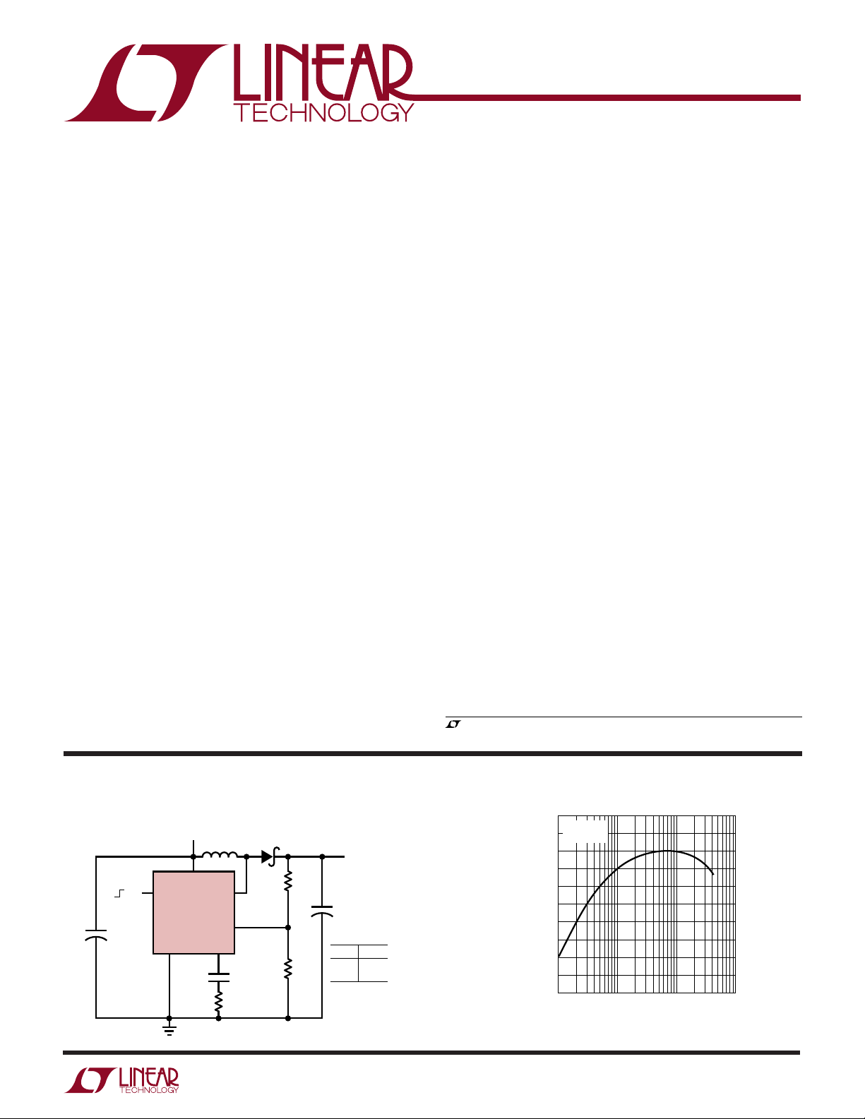
TYPICAL APPLICATIO
5V-to-12V Boost Converter
5V
L1*
MBRS120T3
22µH
5
V
4
ON
OFF
+
C1**
22µF
IN
S/S
LT1373
GND
6, 7
8
V
SW
2
FB
V
C
1
C2
0.01µF
R3
5k
U
12V Output Efficiency
100
D1
†
V
OUT
R1
215k
1%
R2
24.9k
1%
LT1373 • TA01
12V
+
C4**
22µF
†
MAX I
OUT
L1
I
OUT
0.3A
15µH
0.35A
22µH
SUMIDA CD75-220KC (22µH) OR
*
COILCRAFT D03316-153 (15µH)
**
AVX TPSD226M025R0200
VIN = 5V
f = 250kHz
90
80
70
EFFICIENCY (%)
60
50
1
10 100 1000
OUTPUT CURRENT (mA)
LT1373 • TA02
1
Page 2
LT1373
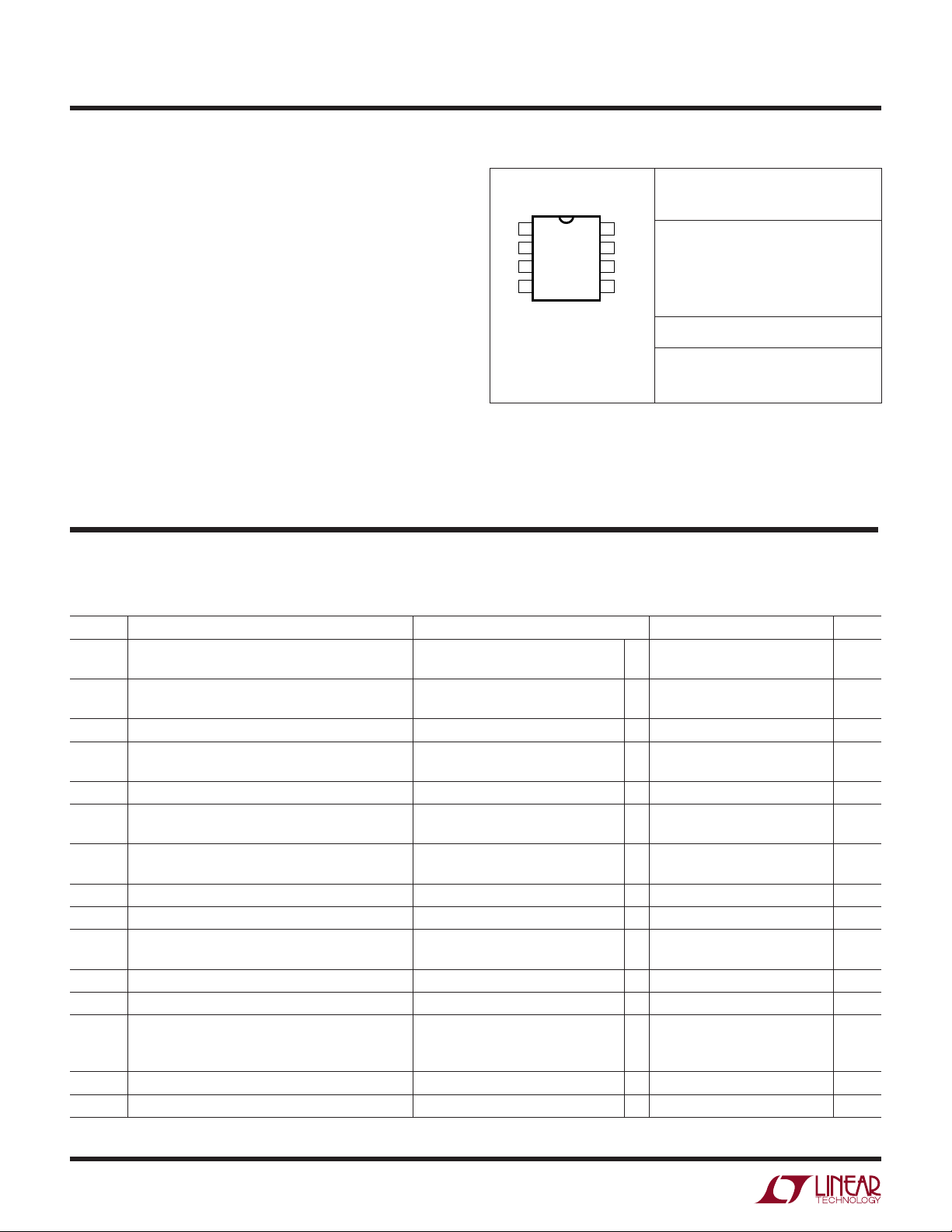
PACKAGE/ORDER I FOR ATIO
UU
W
WWWU
ABSOLUTE AXI U RATI GS
(Note 1)
Supply Voltage ....................................................... 30V
Switch Voltage
LT1373 ............................................................... 35V
LT1373HV .......................................................... 42V
S/S Pin Voltage....................................................... 30V
Feedback Pin Voltage (Transient, 10ms) .............. ±10V
Feedback Pin Current........................................... 10mA
Negative Feedback Pin Voltage
(Transient, 10ms)............................................. ±10V
Operating Junction Temperature Range
Commercial ........................................ 0°C to 125°C*
Industrial ......................................... – 40°C to 125°C
Short Circuit ......................................... 0°C to 150°C
Storage Temperature Range ................ –65°C to 150°C
Lead Temperature (Soldering, 10 sec)................. 300°C
ORDER PART
TOP VIEW
V
1
C
FB
2
NFB
3
S/S
4
N8 PACKAGE
8-LEAD PDIP
T
JMAX
T
JMAX
Consult factory for Military grade parts.
*Units shipped prior to Date Code 9552 are rated at 100°C maximum
operating temperature.
= 125°C, θ
= 125°C, θ
8-LEAD PLASTIC SO
JA
JA
V
8
SW
GND
7
GND S
6
V
5
IN
S8 PACKAGE
= 100°C/ W (N8)
= 120°C/ W (S8)
LT1373CN8
LT1373HVCN8
LT1373CS8
LT1373HVCS8
NUMBER
LT1373IN8
LT1373HVIN8
LT1373IS8
LT1373HVIS8
S8 PART MARKING
1373
1373I
1373H
1373HI
ELECTRICAL CHARACTERISTICS
The ● denotes specifications which apply over the full operating temperature range, otherwise specifications are at TA = 25°C.
VIN = 5V, VC = 0.6V, VFB = V
SYMBOL PARAMETER CONDITIONS MIN TYP MAX UNITS
V
REF
I
FB
V
NFB
I
NFB
g
m
A
V
f Switching Frequency 2.7V ≤ VIN ≤ 25V 225 250 275 kHz
Reference Voltage Measured at Feedback Pin 1.230 1.245 1.260 V
Feedback Input Current VFB = V
Reference Voltage Line Regulation 2.7V ≤ VIN ≤ 25V, VC = 0.8V ● 0.01 0.03 %/V
Negative Feedback Reference Voltage Measured at Negative Feedback Pin –2.51 –2.45 –2.39 V
Negative Feedback Input Current V
Negative Feedback Reference Voltage 2.7V ≤ VIN ≤ 25V, VC = 0.8V ● 0.01 0.05 %/V
Line Regulation
Error Amplifier Transconductance ∆IC = ±5µA 250 375 500 µmho
Error Amplifier Source Current VFB = V
Error Amplifier Sink Current VFB = V
Error Amplifier Clamp Voltage High Clamp, VFB = 1V 1.70 1.95 2.30 V
Error Amplifier Voltage Gain 250 V/V
VC Pin Threshold Duty Cycle = 0% 0.8 1 1.25 V
Maximum Switch Duty Cycle ● 90 95 %
Switch Current Limit Blanking Time 340 500 ns
, VSW, S/S and NFB pins open, unless otherwise noted.
REF
V
= 0.8V ● 1.225 1.245 1.265 V
C
REF
Feedback Pin Open, V
= V
NFB
NFR
– 150mV, VC = 1.5V ● 25 50 90 µA
REF
+ 150mV, VC = 1.5V ● 850 1500 µA
REF
Low Clamp, V
0°C ≤ T
–40°C ≤ T
FB
≤ 125°C ● 210 250 290 kHz
J
≤ 0°C (I Grade) 200 290 kHz
J
= 0.8V ● –2.55 –2.45 –2.35 V
C
= 1.5V 0.25 0.40 0.52 V
50 150 nA
● 275 nA
● –12 –7 –2 µA
● 150 600 µmho
2
Page 3
LT1373
TEMPERATURE (°C)
–50
1.8
INPUT VOLTAGE (V)
2.0
2.2
2.4
2.6
050
100
150
LT1373 • G03
2.8
3.0
–25 25
75
125
ELECTRICAL CHARACTERISTICS
The ● denotes specifications which apply over the full operating temperature range, otherwise specifications are at TA = 25°C.
VIN = 5V, VC = 0.6V, VFB = V
SYMBOL PARAMETER CONDITIONS MIN TYP MAX UNITS
BV Output Switch Breakdown Voltage LT1373 ● 35 47 V
V
SAT
Output Switch “On” Resistance ISW = 1A ● 0.5 0.85 Ω
, VSW, S/S and NFB pins open, unless otherwise noted.
REF
LT1373HV
0°C ≤ T
–40°C ≤ T
≤ 125°C ● 42 47 V
J
≤ 0°C (I Grade) 40 V
J
I
LIM
Switch Current Limit Duty Cycle = 50% ● 1.5 1.9 2.7 A
Duty Cycle = 80% (Note 2)
∆I
∆I
IN
SW
Supply Current Increase During Switch On-Time 10 20 mA/A
Control Voltage to Switch Current 2A/V
Transconductance
Minimum Input Voltage ● 2.4 2.7 V
I
Q
Supply Current 2.7V ≤ VIN ≤ 25V ● 1 1.5 mA
Shutdown Supply Current 2.7V ≤ VIN ≤ 25V, V
0°C ≤ T
–40°C ≤ T
≤ 125°C ● 12 30 µA
J
≤ 0°C (I Grade) 50 µA
J
S/S
≤ 0.6V
Shutdown Threshold 2.7V ≤ VIN ≤ 25V ● 0.6 1.3 2 V
Shutdown Delay ● 5 12 100 µs
S/S Pin Input Current 0V ≤ V
≤ 5V ● –10 15 µA
S/S
Synchronization Frequency Range ● 300 340 kHz
Note 1: Absolute Maximum Ratings are those values beyond which the life
of the device may be impaired.
Note 2: For duty cycles (DC) between 50% and 90%, minimum
guaranteed switch current is given by I
UW
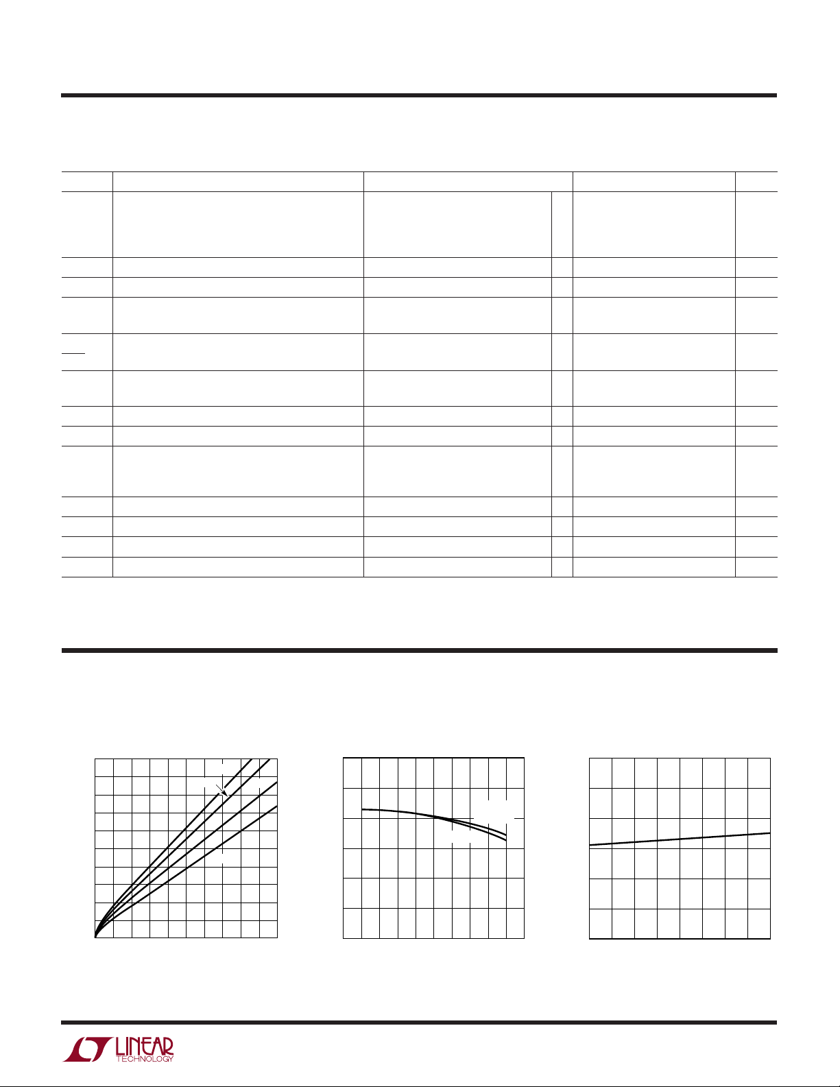
TYPICAL PERFOR A CE CHARACTERISTICS
● 1.3 1.7 2.5 A
= 0.667 (2.75 – DC).
LIM
SWITCH SATURATION VOLTAGE (V)
Switch Saturation Voltage
vs Switch Current
1.0
0.9
0.8
0.7
0.6
0.5
0.4
0.3
0.2
0.1
0
0.2
0.4
0
0.6
SWITCH CURRENT (A)
0.8
100°C
1.0
1.2
150°C
–55°C
1.4
1.6
25°C
1.8
LT1373 • G01
2.0
Switch Current Limit
vs Duty Cycle
3.0
2.5
2.0
1.5
1.0
SWITCH CURRENT LIMIT (A)
0.5
0
20 40 60 80
DUTY CYCLE (%)
–55°C
25°C AND
125°C
LT1373 • G02
Minimum Input Voltage
vs Temperature
10010030 50 70 90
3
Page 4
LT1373
TEMPERATURE (°C)
–50
0
TRANSCONDUCTANCE (µmho)
200
500
0
50
75
LT1373 • G09
100
400
300
–25 25
100
125
150
gm =
∆I (V
C
)
∆V (FB)
TEMPERATURE (°C)
–50
–20
NEGATIVE FEEDBACK INPUT CURRENT (µA)
–12
–14
0
0
50
75
LT1373 • G12
–16
–18
–4
–6
–2
–8
–10
–25 25
100
125
150
V
NFB
= V
NFR
UW
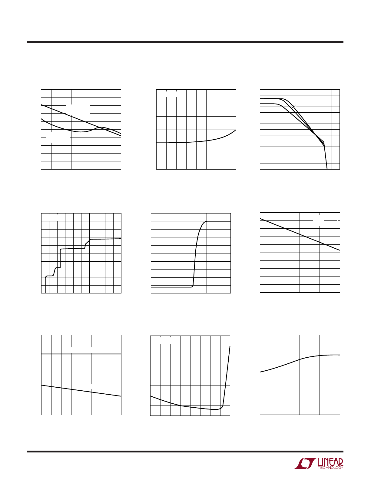
TYPICAL PERFOR A CE CHARACTERISTICS
Shutdown Delay and Threshold
vs Temperature
20
18
SHUTDOWN DELAY (µs)
16
14
12
10
8
6
4
2
0
–50
SHUTDOWN
–25 25
SHUTDOWN
THRESHOLD
DELAY
0
50
TEMPERATURE (°C)
75
S/S Pin Input Current
vs Voltage
5
VIN = 5V
4
3
2
1
0
–1
–2
–3
S/S PIN INPUT CURRENT (µA)
–4
–5
1
2
08
–1
S/S PIN VOLTAGE (V)
5
3
4
Minimum Synchronization
Voltage vs Temperature
)
3.0
f
0
SYNC
–50
= 330kHz
050
–25 25
TEMPERATURE (°C)
P-P
SHUTDOWN THRESHOLD (V)
2.5
2.0
1.5
1.0
0.5
MINIMUM SYNCHRONIZATION VOLTAGE (V
100
75
125
LT1373 • G05
150
100
125
LT1373 • G04
150
2.0
1.8
1.6
1.4
1.2
1.0
0.8
0.6
0.4
0.2
0
Switching Frequency
vs Feedback Pin Voltage
110
100
90
80
70
60
50
40
30
20
SWITCHING FREQUENCY (% OF TYPICAL)
6
7
9
LT1373 • G07
10
0.2
0.3
0.1 0.9
0
FEEDBACK PIN VOLTAGE (V)
0.4
0.5
0.6
0.7
0.8
1.0
LT1373 • G08
Error Amplifier Output Current
vs Feedback Pin Voltage
100
–25
–50
ERROR AMPLIFIER OUTPUT CURRENT (µA)
–75
75
50
25
0
125°C
–0.3 –0.2
FEEDBACK PIN VOLTAGE (V)
25°C
–55°C
V
–0.1 0.1
REF
Error Amplifier Transconductance
vs Temperature
LT1373 • G06
2.4
2.2
2.0
1.8
1.6
1.4
1.2
PIN VOLTAGE (V)
C
1.0
V
0.8
0.6
0.4
4
VC Pin Threshold and High
Clamp Voltage vs Temperature
VC HIGH CLAMP
VC THRESHOLD
–50
–25 25
0
TEMPERATURE (°C)
50
75
100
125
LT1373 • G10
150
Feedback Input Current
vs Temperature
400
VFB = V
–25
REF
0
50
25
TEMPERATURE (°C)
350
300
250
200
150
100
FEEDBACK INPUT CURRENT (nA)
50
0
–50
Negative Feedback Input
Current vs Temperature
75
100
125
LT1373 • G11
150
Page 5
LT1373
U
UU
PI FU CTIO S
VC (Pin 1): Compensation Pin. The VC pin is used for
frequency compensation, current limiting and soft start. It
is the output of the error amplifier and the input of the
current comparator. Loop frequency compensation can be
performed with an RC network connected from the V
to ground.
FB (Pin 2): T
he feedback pin is used for positive output
voltage sensing and oscillator frequency shifting. It is the
inverting input to the error amplifier. The noninverting
input of this amplifier is internally tied to a 1.245V
reference. Load on the FB pin should not exceed 100µA
when the NFB pin is used. See Applications Information.
NFB (Pin 3): The negative feedback pin is used for negative
output voltage sensing. It is connected to the inverting
input of the negative feedback amplifier through a 400k
source resistor.
S/S (Pin 4): Shutdown and Synchronization Pin. The S/S
pin is logic level compatible. Shutdown is active low and
the shutdown threshold is typically 1.3V. For normal
operation, pull the S/S pin high, tie it to V
or leave it
IN
C
pin
floating. To synchronize switching, drive the S/S pin between 300kHz and 340kHz.
V
(Pin 5): Input Supply Pin. Bypass VIN with 10µF or
IN
more. The part goes into undervoltage lockout when V
IN
drops below 2.5V. Undervoltage lockout stops switching
and pulls the V
pin low.
C
GND S (Pin 6): The ground sense pin is a “clean” ground.
The internal reference, error amplifier and negative feedback amplifier are referred to the ground sense pin. Connect it to ground. Keep the ground path connection to the
output resistor divider and the V
compensation network
C
free of large ground currents.
GND (Pin 7): The ground pin is the emitter connection of
the power switch and has large currents flowing through it.
It should be connected directly to a good quality ground
plane.
V
(Pin 8): The switch pin is the collector of the power
SW
switch and has large currents flowing through it. Keep the
traces to the switching components as short as possible to
minimize radiation and voltage spikes.
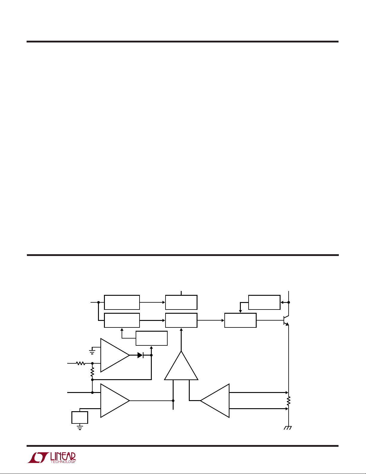
BLOCK DIAGRA
S/S
FEEDBACK
NFB
FB
400k
200k
1.245V
REF
GND SENSE
W
SHUTDOWN
DELAY AND RESET
SYNC
+
NEGATIVE
AMP
–
–
ERROR
AMP
+
250kHz
OSC
5:1 FREQUENCY
SHIFT
V
IN
LOW DROPOUT
2.3V REG
LOGIC DRIVER
COMP
CURRENT
AMP
V
C
AV ≈ 6
SW
ANTI-SAT
SWITCH
+
0.08Ω
–
GND LT1373 • BD
5
Page 6
LT1373
OPERATIO
U
The LT1373 is a current mode switcher. This means that
switch duty cycle is directly controlled by switch current
rather than by output voltage. Referring to the Block
Diagram, the switch is turned “On” at the start of each
oscillator cycle. It is turned “Off” when switch current
reaches a predetermined level. Control of output voltage
is obtained by using the output of a voltage sensing error
amplifier to set current trip level. This technique has
several advantages. First, it has immediate response to
input voltage variations, unlike voltage mode switchers
which have notoriously poor line transient response.
Second, it reduces the 90° phase shift at mid-frequencies
in the energy storage inductor. This greatly simplifies
closed-loop frequency compensation under widely varying input voltage or output load conditions. Finally, it
allows simple pulse-by-pulse current limiting to provide
maximum switch protection under output overload or
short conditions. A low dropout internal regulator provides a 2.3V supply for all internal circuitry. This low
dropout design allows input voltage to vary from 2.7V to
25V with virtually no change in device performance. A
250kHz oscillator is the basic clock for all internal timing.
It turns “On” the output switch via the logic and driver
circuitry. Special adaptive anti-sat circuitry detects onset
of saturation in the power switch and adjusts driver
current instantaneously to limit switch saturation. This
minimizes driver dissipation and provides very rapid
turn-off of the switch.
A 1.245V bandgap reference biases the positive input of
the error amplifier. The negative input of the amplifier is
brought out for positive output voltage sensing. The error
amplifier has nonlinear transconductance to reduce out-
put overshoot on start-up or overload recovery. When
the feedback voltage exceeds the reference by 40mV,
error amplifier transconductance increases ten times,
which reduces output overshoot. The feedback input also
invokes oscillator frequency shifting, which helps protect components during overload conditions. When the
feedback voltage drops below 0.6V, the oscillator frequency is reduced 5:1. Lower switching frequency allows
full control of switch current limit by reducing minimum
switch duty cycle.
Unique error amplifier circuitry allows the LT1373 to
directly regulate negative output voltages. The negative
feedback amplifier’s 400k source resistor is brought out
for negative output voltage sensing. The NFB pin regulates
at –2.45V while the amplifier output internally drives the
FB pin to 1.245V. This architecture, which uses the same
main error amplifier, prevents duplicating functions and
maintains ease of use. (Consult Linear Technology Marketing for units that can regulate down to –1.25V.)
The error signal developed at the amplifier output is
brought out externally. This pin (VC) has three different
functions. It is used for frequency compensation, current
limit adjustment and soft starting. During normal regulator operation this pin sits at a voltage between 1V (low
output current) and 1.9V (high output current). The error
amplifier is a current output (gm) type, so this voltage can
be externally clamped for lowering current limit. Likewise, a capacitor coupled external clamp will provide soft
start. Switch duty cycle goes to zero if the VC pin is pulled
below the control pin threshold, placing the LT1373 in an
idle mode.
WUUU
APPLICATIO S I FOR ATIO
Positive Output Voltage Setting
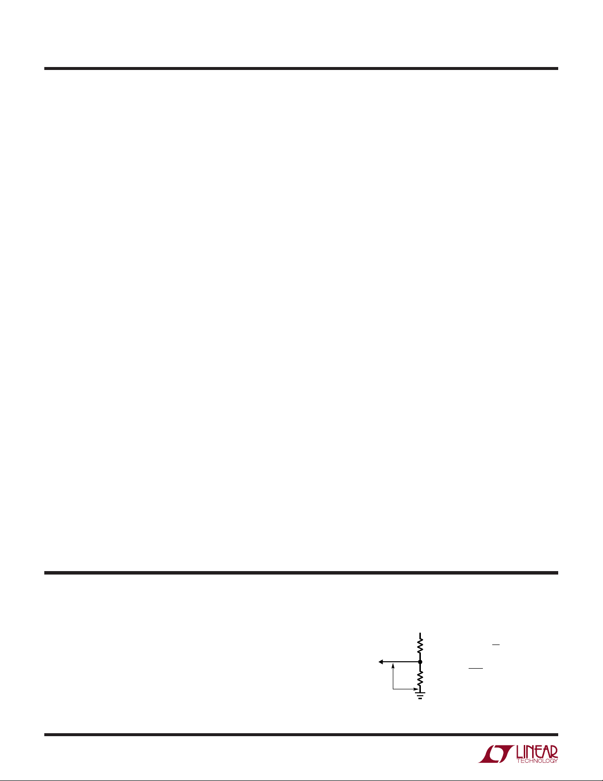
The LT1373 develops a 1.245V reference (V
) from the
REF
FB pin to ground. Output voltage is set by connecting the
FB pin to an output resistor divider (Figure 1). The FB pin
bias current represents a small error and can usually be
ignored for values of R2 up to 25k. The suggested value for
R2 is 24.9k. The NFB pin is normally left open for positive
output applications.
6
V
OUT
= V
V
R1
OUT
FB
PIN
V
REF
Figure 1. Positive Output Resistor Divider
R1 = R2
R2
R1
1 +
REF
()
R2
V
OUT
– 1
()
1.245
LT1373 • F01
Page 7
WUUU
APPLICATIO S I FOR ATIO
LT1373
Negative Output Voltage Setting
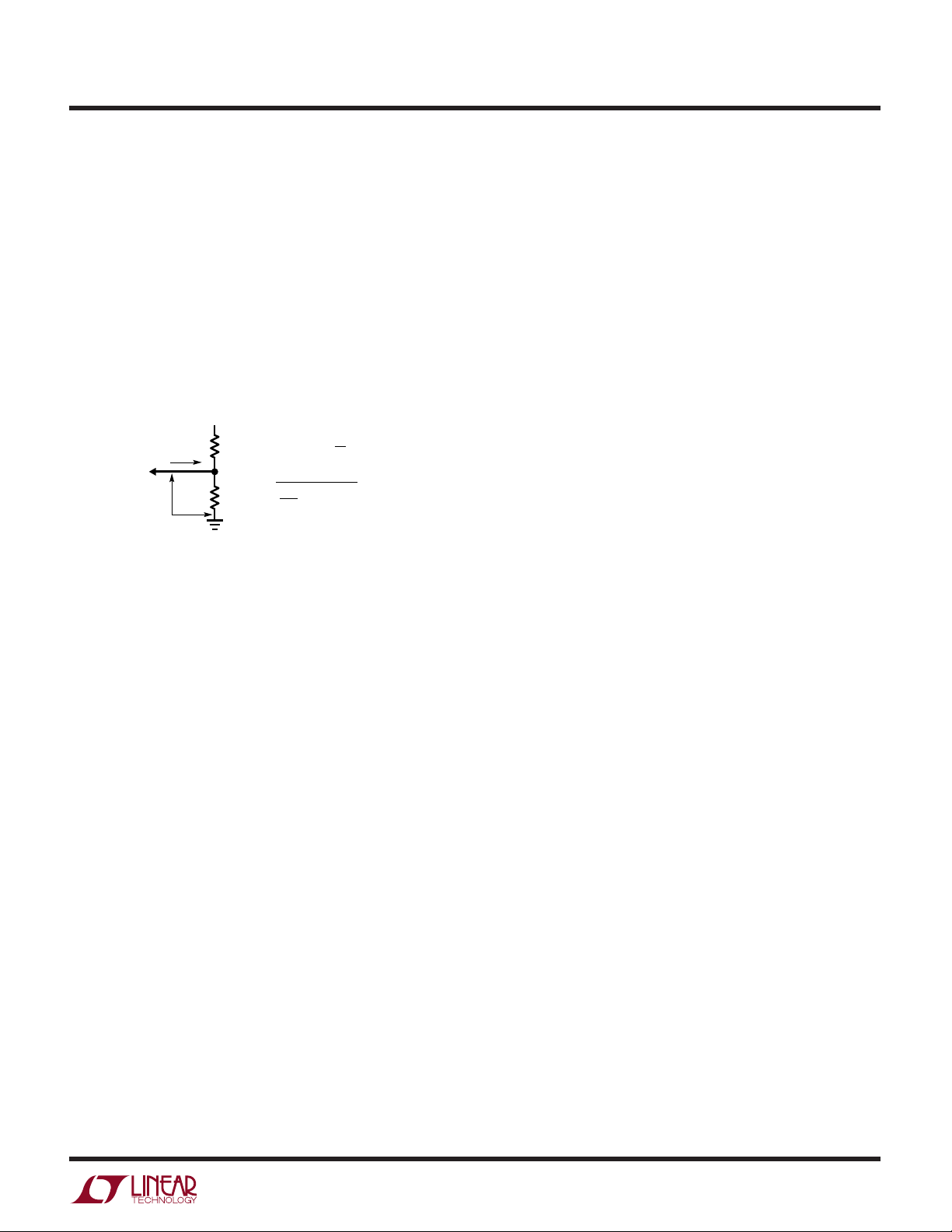
The LT1373 develops a –2.45V reference (V
) from the
NFR
NFB pin to ground. Output voltage is set by connecting the
NFB pin to an output resistor divider (Figure 2). The –7µA
NFB pin bias current (I
) can cause output voltage errors
NFB
and should not be ignored. This has been accounted for in
the formula in Figure 2. The suggested value for R2 is
2.49k. The FB pin is normally left open for negative output
applications. See Dual Polarity Output Voltage Sensing for
limitations of FB pin loading when using the NFB pin.
–V
OUT
= V
–V
R1
I
NFB
PIN
NFB
V
NFR
Figure 2. Negative Output Resistor Divider
OUT
V
R1 =
R2
2.45
()
R2
R1
+ I
NFB
()
R2
– 2.45
OUT
+ (7 • 10–6)
(R1)1 +
NFB
LT1373 • F02
Dual Polarity Output Voltage Sensing
Certain applications benefit from sensing both positive
and negative output voltages. One example is the Dual
Output Flyback Converter with Overvoltage Protection
circuit shown in the Typical Applications section. Each
output voltage resistor divider is individually set as described above. When both the FB and NFB pins are used,
the LT1373 acts to prevent either output from going
beyond its set output voltage. For example in this application, if the positive output were more heavily loaded than
the negative, the negative output would be greater and
would regulate at the desired set-point voltage. The positive output would sag slightly below its set-point voltage.
This technique prevents either output from going unregulated high at no load. Please note that the load on the FB
pin should not exceed 100µA when the NFB pin is used.
This situation occurs when the resistor dividers are used
at both FB
and
NFB. True load on FB is not the full divider
current unless the positive output is shorted to ground.
See Dual Output Flyback Converter application.
Shutdown and Synchronization
The dual function S/S pin provides easy shutdown and
synchronization. It is logic level compatible and can be
pulled high, tied to VIN or left floating for normal operation.
A logic low on the S/S pin activates shutdown, reducing
the part’s supply current to 12µA. Typical synchronization
range is from 1.05 and 1.8 times the part’s natural switching frequency, but is only guaranteed between 300kHz and
340kHz. A 12µs resetable shutdown delay network guar-
antees the part will not go into shutdown while receiving
a synchronization signal.
Caution should be used when synchronizing above
330kHz because at higher sync frequencies the amplitude of the internal slope compensation used to prevent
subharmonic switching is reduced. This type of
subharmonic switching only occurs when the duty cycle
of the switch is above 50%. Higher inductor values will
tend to eliminate problems.
Thermal Considerations
Care should be taken to ensure that the worst-case input
voltage and load current conditions do not cause excessive die temperatures. The packages are rated at 120°C/W
for SO (S8) and 130°C/W for PDIP (N8).
Average supply current (including driver current) is:
IIN = 1mA + DC (ISW/60 + ISW • 0.004)
ISW = switch current
DC = switch duty cycle
Switch power dissipation is given by:
PSW = (ISW)2 • RSW • DC
RSW = output switch “On” resistance
Total power dissipation of the die is the sum of supply
current times supply voltage plus switch power:
P
D(TOTAL)
= (IIN • VIN) + P
SW
Choosing the Inductor
For most applications the inductor will fall in the range of
10µH to 50µH. Lower values are chosen to reduce physical
size of the inductor. Higher values allow more output
current because they reduce peak current seen by the
power switch which has a 1.5A limit. Higher values also
reduce input ripple voltage, and reduce core loss.
When choosing an inductor you might have to consider
maximum load current, core and copper losses, allowable
7
Page 8
LT1373
WUUU
APPLICATIO S I FOR ATIO
component height, output voltage ripple, EMI, fault current in the inductor, saturation, and of course, cost. The
following procedure is suggested as a way of handling
these somewhat complicated and conflicting requirements.
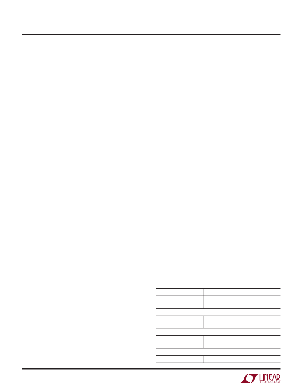
1. Assume that the average inductor current (for a boost
converter) is equal to load current times V
OUT/VIN
and
decide whether or not the inductor must withstand
continuous overload conditions. If average inductor
current at maximum load current is 0.5A, for instance,
a 0.5A inductor may not survive a continuous 1.5A
overload condition. Also, be aware that boost converters are not short-circuit protected, and that under
output short conditions, inductor current is limited only
by the available current of the input supply.
2. Calculate peak inductor current at full load current to
ensure that the inductor will not saturate. Peak current
can be significantly higher than output current, especially with smaller inductors and lighter loads, so don’t
omit this step. Powered iron cores are forgiving because they saturate softly, whereas ferrite cores saturate abruptly. Other core materials fall in between
somewhere. The following formula assumes continuous mode operation, but it errors only slightly on the
high side for discontinuous mode, so it can be used for
all conditions.
V
I
= I
PEAK
V
IN
OUT
= minimum input voltage
OUT
•
V
IN
V
IN (VOUT – VIN
+
2(f)(L)(V
OUT
)
)
f = 250kHz switching frequency
inductor gets too hot, wire insulation will melt and cause
turn-to-turn shorts). Keep in mind that all good things
like high efficiency, low profile and high temperature
operation will increase cost, sometimes dramatically.
5. After making an initial choice, consider the secondary
things like output voltage ripple, second sourcing, etc.
Use the experts in the Linear Technology application
department if you feel uncertain about the final choice.
They have experience with a wide range of inductor
types and can tell you about the latest developments in
low profile, surface mounting, etc.
Output Capacitor
The output capacitor is normally chosen by its effective
series resistance (ESR), because this is what determines
output ripple voltage. At 500kHz, any polarized capacitor
is essentially resistive. To get low ESR takes
volume
, so
physically smaller capacitors have high ESR. The ESR
range for typical LT1373 applications is 0.05Ω to 0.5Ω. A
typical output capacitor is an AVX type TPS, 22µF at 25V,
with a guaranteed ESR less than 0.2Ω. This is a “D” size
surface mount solid tantalum capacitor. TPS capacitors
are specially constructed and tested for low ESR, so they
give the lowest ESR for a given volume. To further reduce
ESR, multiple output capacitors can be used in parallel.
The value in microfarads is not particularly critical and
values from 22µF to greater than 500µF work well, but you
cannot cheat mother nature on ESR. If you find a tiny 22µF
solid tantalum capacitor, it will have high ESR and output
ripple voltage will be terrible. Table 1 shows some typical
solid tantalum surface mount capacitors.
3. Decide if the design can tolerate an “open” core geometry like a rod or barrel, which have high magnetic field
radiation, or whether it needs a closed core like a toroid
to prevent EMI problems. One would not want an open
core next to a magnetic storage media for instance!
This is a tough decision because the rods or barrels are
temptingly cheap and small, and there are no helpful
guidelines to calculate when the magnetic field radiation will be a problem.
4. Start shopping for an inductor which meets the requirements of core shape, peak current (to avoid saturation),
average current (to limit heating), and fault current, (if the
8
Table 1. Surface Mount Solid Tantalum Capacitor
ESR and Ripple Current
E CASE SIZE ESR (MAX Ω) RIPPLE CURRENT (A)
AVX TPS, Sprague 593D 0.1 to 0.3 0.7 to 1.1
AVX TAJ 0.7 to 0.9 0.4
D CASE SIZE
AVX TPS, Sprague 593D 0.1 to 0.3 0.7 to 1.1
AVX TAJ 0.9 to 2.0 0.36 to 0.24
C CASE SIZE
AVX TPS 0.2 (Typ) 0.5 (Typ)
AVX TAJ 1.8 to 3.0 0.22 to 0.17
B CASE SIZE
AVX TAJ 2.5 to 10 0.16 to 0.08
Page 9

WUUU
APPLICATIO S I FOR ATIO
LT1373
Many engineers have heard that solid tantalum capacitors
are prone to failure if they undergo high surge currents.
This is historically true and type TPS capacitors are
specially tested for surge capability, but surge ruggedness
is not a critical issue with the
tantalum capacitors fail during very high
which do not occur at the output of regulators. High
discharge
dead shorted, do not harm the capacitors.
Single inductor boost regulators have large RMS ripple
current in the output capacitor, which must be rated to
handle the current. The formula to calculate this is:
Output Capacitor Ripple Current (RMS)
I
Input Capacitors
The input capacitor of a boost converter is less critical due
to the fact that the input current waveform is triangular,
and does not contain large squarewave currents as is
found in the output capacitor. Capacitors in the range of
10µF to 100µF with an ESR (effective series resistance) of
0.3Ω or less work well up to a full 1.5A switch current.
Higher ESR capacitors may be acceptable at low switch
currents. Input capacitor ripple current for boost converter is:
I
f = 250kHz switching frequency
The input capacitor can see a very high surge current when
a battery or high capacitance source is connected “live”,
and solid tantalum capacitors can fail under this condition.
Several manufacturers have developed a line of solid
tantalum capacitors specially tested for surge capability
(AVX TPS series, for instance), but even these units may
fail if the input voltage approaches the maximum voltage
rating of the capacitor. AVX recommends derating capacitor voltage by 2:1 for high surge applications. Ceramic and
surges, such as when the regulator output is
RIPPLE
RIPPLE
(RMS) = I
= I
0.3(V
=
IN
(f)(L)(V
OUT
OUT
)(V
OUT
OUT
output
DC
1 – DC
V
OUT – VIN
V
– VIN)
)
capacitor. Solid
turn-on
IN
surges,
aluminum electrolytic capacitors may also be used and
have a high tolerance to turn-on surges.
Ceramic Capacitors
Higher value, lower cost ceramic capacitors are now
becoming available in smaller case sizes. These are tempting for switching regulator use because of their very low
ESR. Unfortunately, the ESR is so low that it can cause
loop stability problems. Solid tantalum capacitor ESR
generates a loop “zero” at 5kHz to 50kHz that is instrumental in giving acceptable loop phase margin. Ceramic capacitors remain capacitive to beyond 300kHz and usually
resonate with their ESL before ESR becomes effective.
They are appropriate for input bypassing because of their
high ripple current ratings and tolerance of turn-on surges.
Linear Technology plans to issue a Design Note on the use
of ceramic capacitors in the near future.
Output Diode
The suggested output diode (D1) is a 1N5818 Schottky or
its Motorola equivalent, MBR130. It is rated at 1A average
forward current and 30V reverse voltage. Typical forward
voltage is 0.42V at 1A. The diode conducts current only
during switch-off time. Peak reverse voltage for boost
converters is equal to regulator output voltage. Average
forward current in normal operation is equal to output
current.
Frequency Compensation
Loop frequency compensation is performed on the output
of the error amplifier (VC pin) with a series RC network. The
main pole is formed by the series capacitor and the output
impedance (≈1MΩ) of the error amplifier. The pole falls in
the range of 5Hz to 30Hz. The series resistor creates a
“zero” at 2kHz to 10kHz, which improves loop stability and
transient response. A second capacitor, typically one tenth
the size of the main compensation capacitor, is sometimes
used to reduce the switching frequency ripple on the V
pin. VC pin ripple is caused by output voltage ripple
attenuated by the output divider and multiplied by the error
amplifier. Without the second capacitor, VC pin ripple is:
VC Pin Ripple =
1.245(V
RIPPLE
V
OUT
)(gm)(RC)
C
9
Page 10
LT1373
WUUU
APPLICATIO S I FOR ATIO
V
= output ripple (V
RIPPLE
P-P
)
gm = error amplifier transconductance (≈375µmho)
RC = series resistor on VC pin
V
= DC output voltage
OUT
To prevent irregular switching, VC pin ripple should be
kept below 50mV
. Worst-case VC pin ripple occurs at
P-P
maximum output load current and will also be increased if
poor quality (high ESR) output capacitors are used. The
addition of a 0.001µF capacitor on the VC pin reduces
switching frequency ripple to only a few millivolts. A low
value for RC will also reduce VC pin ripple, but loop phase
margin may be inadequate.
Switch Node Considerations
For maximum efficiency, switch rise and fall time are made
as short as possible. To prevent radiation and high frequency resonance problems, proper layout of the components connected to the switch node is essential. B field
(magnetic) radiation is minimized by keeping output diode, switch pin and output bypass capacitor leads as short
as possible. E field radiation is kept low by minimizing the
length and area of all traces connected to the switch pin.
A ground plane should always be used under the switcher
circuitry to prevent interplane coupling.
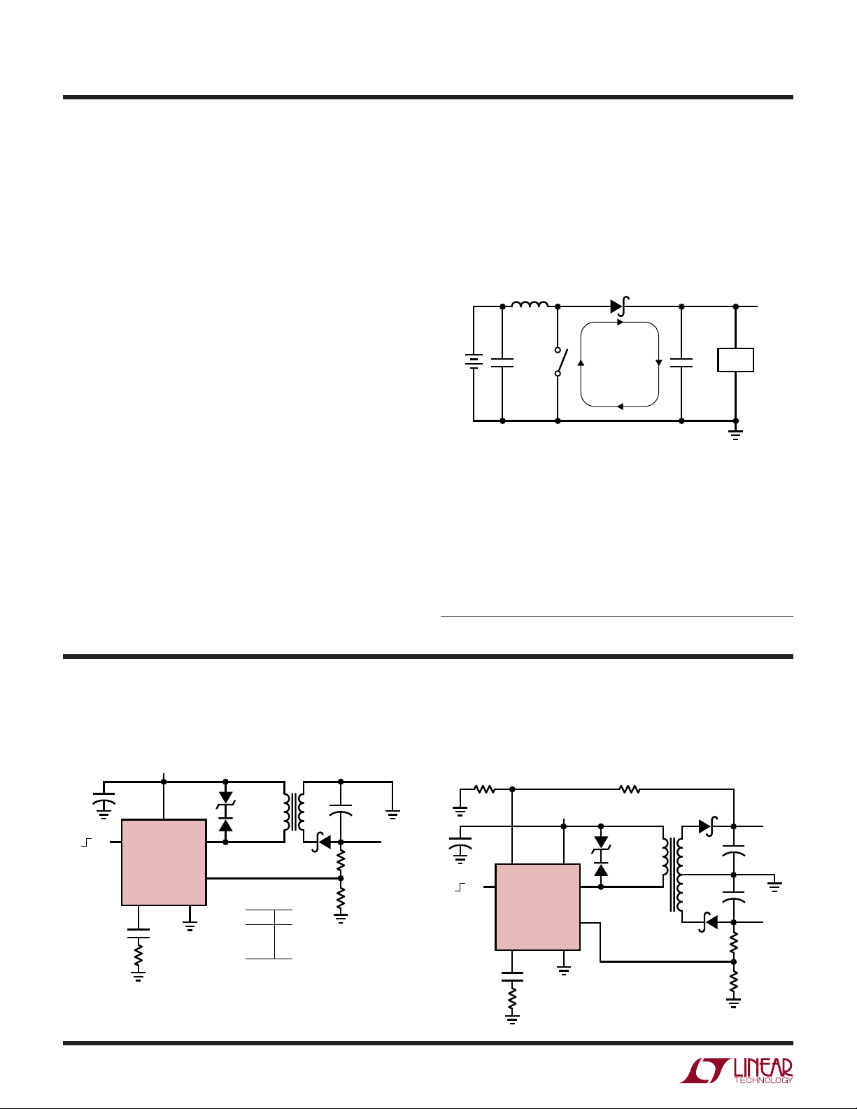
The high speed switching current path is shown schematically in Figure 3. Minimum lead length in this path is
essential to ensure clean switching and low EMI. The path
including the switch, output diode and output capacitor is
the only one containing nanosecond rise and fall times.
Keep this path as short as possible.
SWITCH
L1
NODE
V
IN
HIGH
FREQUENCY
CIRCULATING
PATH
LOAD
V
OUT
LT1373 • F03
Figure 3
More Help
For more detailed information on switching regulator
circuits, please see AN19. Linear Technology also offers a
computer software program, SwitcherCADTM, to assist in
designing switching converters. In addition, our applications department is always ready to lend a helping hand.
SwitcherCAD is a trademark of Linear Technology Corporation.
U
TYPICAL APPLICATIONS N
Positive-to-Negative Converter with Direct Feedback
V
IN
OFF
+
ON
4
C1
22µF
2.7V TO 16V
S/S
LT1373
V
C
1
R1
5k
5
V
IN
C2
0.01µF
D2
P6KE-15A
D3
1N4148
8
V
SW
3
NFB
GND
6, 7
*COILTRONICS CTX20-2 (407) 241-7876
†
214
•
MBRS130LT3
MAX I
OUT
V
I
IN
OUT
3V
0.3A
5V
0.5A
9V
0.75A
T1*
•
3
D1
Dual Output Flyback Converter with Overvoltage Protection
R2
275k
1%
+
C3
47µF
+
†
R2
2.55k
1%
R3
2.49k
1%
–V
OUT
–5V
LT1373 • TA03
OFF
ON
C1
100µF
4
S/S
FB
V
C
1
V
IN
4.75V TO 13V
52
V
IN
V
SW
LT1373
NFB
GND
6, 7
C2
0.01µF
R3
5k
*DALE LPE-4841-100MB (605) 665-9301
R1
302.6k
1%
MBRS140T3
T1*
2, 3
5
+
4
8
+
1
6, 7
•
•
•
MBRS140T3
P6KE-20A
1N4148
8
3
C3
47µF
C4
47µF
R4
12.4k
1%
R5
2.49k
1%
V
OUT
15V
–V
OUT
–15V
LT1373 • TA04
10
Page 11
TYPICAL APPLICATIO S
V
IN
5V
C1
22µF
10V
*
**
U
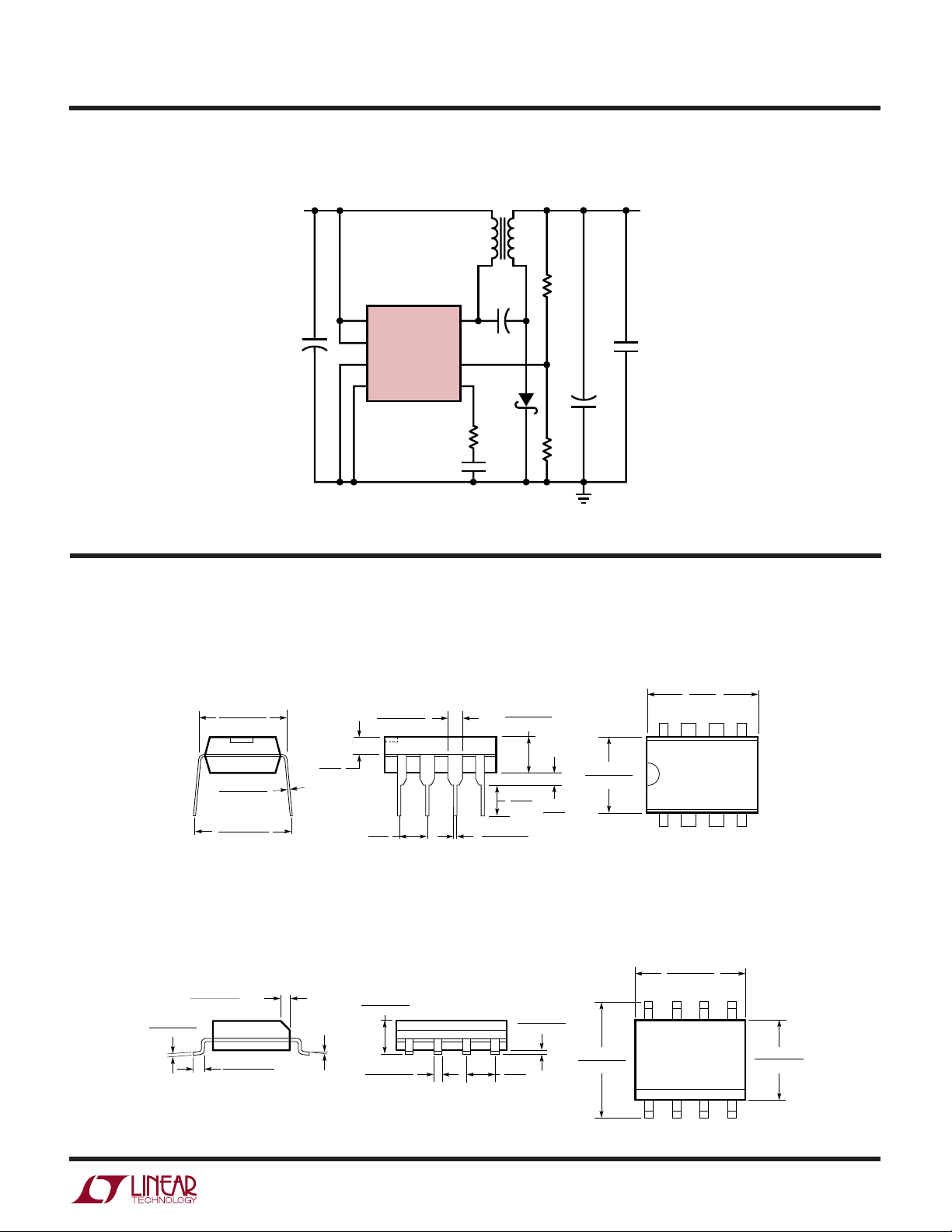
Low Ripple 5V to –3V “Cuk”† Converter
L1*
2
••
C2
47µF
5
V
4
7
6
IN
S/S
GND
GND S
LT1373
+
SUMIDA CLS62-100L
MOTOROLA MBR0520LT3
†
PATENTS MAY APPLY
V
NFB
SW
V
C
16V
8
+
3
1
D1**
R4
5k
C4
0.01µF
LT1373
V
OUT
C3
47µF
16V
–3V
250mA
C6
0.1µF
LT1373 • TA05
3
41
R1
1k
1%
+
R2
5.49k
1%
PACKAGE DESCRIPTION
0.300 – 0.325
(7.620 – 8.255)
0.065
(1.651)
0.009 – 0.015
(0.229 – 0.381)
+0.035
0.325
–0.015
+0.889
8.255
()
–0.381
*THESE DIMENSIONS DO NOT INCLUDE MOLD FLASH OR PROTRUSIONS.
MOLD FLASH OR PROTRUSIONS SHALL NOT EXCEED 0.010 INCH (0.254mm)
0.010 – 0.020
(0.254 – 0.508)
0.008 – 0.010
(0.203 – 0.254)
*
DIMENSION DOES NOT INCLUDE MOLD FLASH. MOLD FLASH
SHALL NOT EXCEED 0.006" (0.152mm) PER SIDE
**
DIMENSION DOES NOT INCLUDE INTERLEAD FLASH. INTERLEAD
FLASH SHALL NOT EXCEED 0.010" (0.254mm) PER SIDE
× 45°
0.016 – 0.050
(0.406 – 1.270)
TYP
0°– 8° TYP
U
Dimensions in inches (millimeters) unless otherwise noted.
N8 Package
8-Lead PDIP (Narrow 0.300)
(LTC DWG # 05-08-1510)
0.045 – 0.065
(1.143 – 1.651)
0.100
(2.54)
BSC
0.130 ± 0.005
(3.302 ± 0.127)
0.125
(3.175)
MIN
0.018 ± 0.003
(0.457 ± 0.076)
0.020
(0.508)
MIN
0.255 ± 0.015*
(6.477 ± 0.381)
S8 Package
8-Lead Plastic Small Outline (Narrow 0.150)
(LTC DWG # 05-08-1610)
0.053 – 0.069
(1.346 – 1.752)
0.014 – 0.019
(0.355 – 0.483)
TYP
0.004 – 0.010
(0.101 – 0.254)
0.050
(1.270)
BSC
0.228 – 0.244
(5.791 – 6.197)
0.400*
(10.160)
MAX
876
1234
0.189 – 0.197*
(4.801 – 5.004)
7
8
1
2
6
3
5
N8 1098
5
0.150 – 0.157**
(3.810 – 3.988)
4
SO8 1298
Information furnished by Linear Technology Corporation is believed to be accurate and reliable.
However, no responsibility is assumed for its use. Linear Technology Corporation makes no representation that the interconnection of circuits as described herein will not infringe on existing patent rights.
11
Page 12
LT1373
TYPICAL APPLICATIO S
U
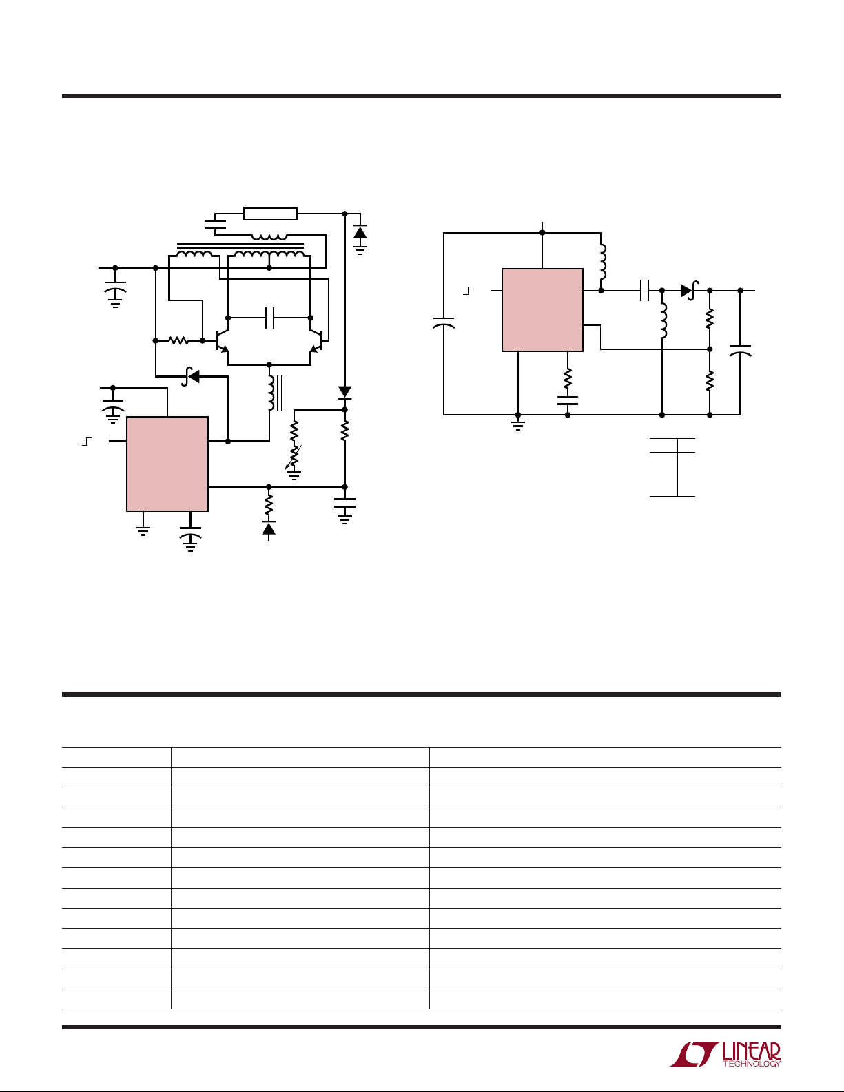
90% Efficient CCFL Supply
C2
27pF
V
IN
4.5V
+
TO 30V
2.7V TO
5.5V
OFF
C1 = WIMA MKP-20
L1 = COILCRAFT D03316-104
Q1, Q2 = ZETEX ZTX849 OR ROHM 2SC5001
T1 = COILTRONICS CTX 110609
* = 1% FILM RESISTOR
DO NOT SUBSTITUTE COMPONENTS
COILTRONICS (407) 241-7876
COILCRAFT (708) 639-6400
ON
10µF
330Ω
1N5818
+
2.2µF
S/S
GND
5
V
IN
LT1373
V
SW
V
FB
V
C
16, 7
+
5mA MAX
LAMP
10
T1
12345
C1
0.1µF
Q1
84
2
2µF
OPTIONAL REMOTE
DIMMING
CCFL BACKLIGHT APPLICATION CIRCUITS
CONTAINED IN THIS DATA SHEET ARE
COVERED BY U.S. PATENT NUMBER 5408162
AND OTHER PATENTS PENDING
L1
100µH
22k
1N4148
Q2
562Ω*
20k
DIMMING
D2
1N4148
10k
0.1µF
LT1372 • TA06
D1
1N4148
Two Li-Ion Cells to 5V SEPIC Conveter
V
IN
4V TO 9V
FB
1
R1
5k
8
2
C4
0.01µF
•
L1A
33µH
C2
2.2µF
MBRS130LT3
•
L1B
33µH
†
MAX I
OUT
I
OUT
0.45A
0.55A
0.65A
0.72A
D1
†
V
OUT
+
5V
C3
100µF
10V
LT1373 • TA07
R2
75k
1%
R3
24.9k
1%
V
IN
4V
5V
7V
9V
5
V
S/S
GND
LT1373
6, 7
IN
V
SW
V
C
4
ON
OFF
C1
+
33µF
20V
C1 = AVX TPSD 336M020R0200
C2 = TOKIN 1E225ZY5U-C203-F
C3 = AVX TPSD 107M010R0100
L1 = COILTRONICS CTX33-2, SINGLE
INDUCTOR WITH TWO WINDINGS
RELATED PARTS
PART NUMBER DESCRIPTION COMMENTS
LT1172 100kHz 1.25A Boost Switching Regulator Also for Flyback, Buck and Inverting Configurations
LTC®1265 13V 1.2A Monolithic Buck Converter Includes PMOS Switch On-Chip
LT1302 Micropower 2A Boost Converter Converts 2V to 5V at 600mA
LT1308A/LT1308B 600kHz 2A Switch DC/DC Converter 5V at 1A from a Single Li-Ion Cell
LT1370 500kHz High Efficiency 6A Boost Converter 6A, 0.065Ω Internal Switch
LT1372 500kHz 1.5A Boost Switching Regulator Also Regulates Negative Flyback Outputs
LT1374 4.5A, 500kHz Step-Down Converter 4.5A, 0.07Ω Internal Switch
LT1376 500kHz 1.5A Buck Switching Regulator Handles Up to 25V Inputs
LT1377 1MHz 1.5A Boost Switching Regulator Only 1MHz Integrated Switching Regulator Available
LT1613 1.4MHz Switching Regulator in 5-Lead SOT-23 5V at 200mA from 4.4V Input
LT1615 Micropower Step-Up DC/DC in 5-Lead SOT-23 20µA IQ, 36V, 350mA Switch
LT1949 600kHz, 1A Switch PWM DC/DC Converter 1.1A, 0.5Ω, 30V Internal Switch, VIN as Low as 1.5V
1373fb LT/TP 0200 2K REV B • PRINTED IN THE USA
LINEAR TECHNOLOGY CORPORATION 1995
12
Linear Technology Corporation
1630 McCarthy Blvd., Milpitas, CA 95035-7417
(408) 432-1900 ● FAX: (408) 434-0507
●
www.linear-tech.com
 Loading...