

Page 1
FEATURES
■
Input Common Mode Range Includes Both Rails
■
Output Swings Rail-to-Rail
■
Low Input Offset Voltage: 150µV
■
High Common Mode Rejection Ratio: 90dB
■
High A
■
Low Input Bias Current: 10nA
■
Wide Supply Range: 1.8V to ±15V
■
Low Supply Current: 375µA per Amplifier
■
High Output Drive: 30mA
■
400kHz Gain-Bandwidth Product
■
Slew Rate: 0.13V/µs
■
Stable for Capacitive Loads up to 1000pF
: >1V/µV Driving 10kΩ Load
VOL
U
APPLICATIONS
■
Rail-to-Rail Buffer Amplifiers
■
Low Voltage Signal Processing
■
Supply Current Sensing at Either Rail
■
Driving A/D Converters
, LTC and LT are registered trademarks of Linear Technology Corporation.
LT1366/LT1367
LT1368/LT1369
Dual and Quad Precision
Rail-to-Rail Input and Output
Op Amps
U
DESCRIPTION
The LT®1366/LT1367/LT1368/LT1369 are dual and quad
bipolar op amps which combine rail-to-rail input and
output operation with precision specifications. These op
amps maintain their characteristics over a supply range of
1.8V to 36V. Operation is specified for 3V, 5V and ±15V
supplies. Input offset voltage is typically 150µV, with an
open-loop gain A
Common mode rejection is typically 90dB over the full railto-rail input range, and supply rejection is 110dB.
The LT1366/LT1367 have conventional compensation
which assures stability for capacitive loads of 1000pF or
less. The LT1368/LT1369 have compensation that
requires a 0.1µF output capacitor, which improves the
amplifier’s supply rejection and reduces output impedance at high frequencies. The output capacitor’s filtering
action reduces high frequency noise, which is beneficial
when driving A/D converters.
The LT1366/LT1368 are available in plastic 8-pin PDIP and
8-lead SO packages with the standard dual op amp pinout.
The LT1367/LT1369 feature the standard quad pinout,
which is available in a plastic 14-lead SO package. These
devices can be used as plug-in replacements for many
standard op amps to improve input/output range and
precision.
of 1 million while driving a 10k load.
VOL
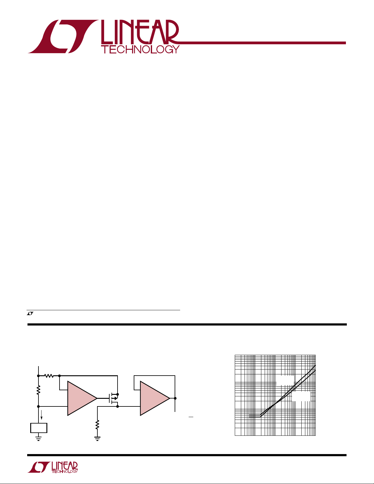
TYPICAL APPLICATION
Positive Supply Rail Current Sense
V
CC
R1
200Ω
LOAD
Rs
0.2Ω
I
LOAD
–
1/2 LT1366
+
R2
20k
Q1
TP0610L
U
–
1/2 LT1366
+
VO = I
= I
LOAD
LOAD
• RS
• 20Ω
R2
(
R1
1366 TA01
Output Saturation Voltage vs Load Current
1000
100
S
– V
OUT
V
10
)
SATURATION VOLTAGE (mV)
1
0.001 0.1 1 10
0.01
LOAD CURRENT (mA)
POSITIVE
RAIL
NEGATIVE
RAIL
1366 TA02
1
Page 2
LT1366/LT1367
LT1368/LT1369
WW
W
U
ABSOLUTE MAXIMUM RATINGS
Total Supply Voltage (V+ to V–) ............................. 36V
Input Current ..................................................... ±15mA
Output Short-Circuit Duration (Note 1)........ Continuous
Operating Temperature Range .............. –40°C to 85°C
U
W
U
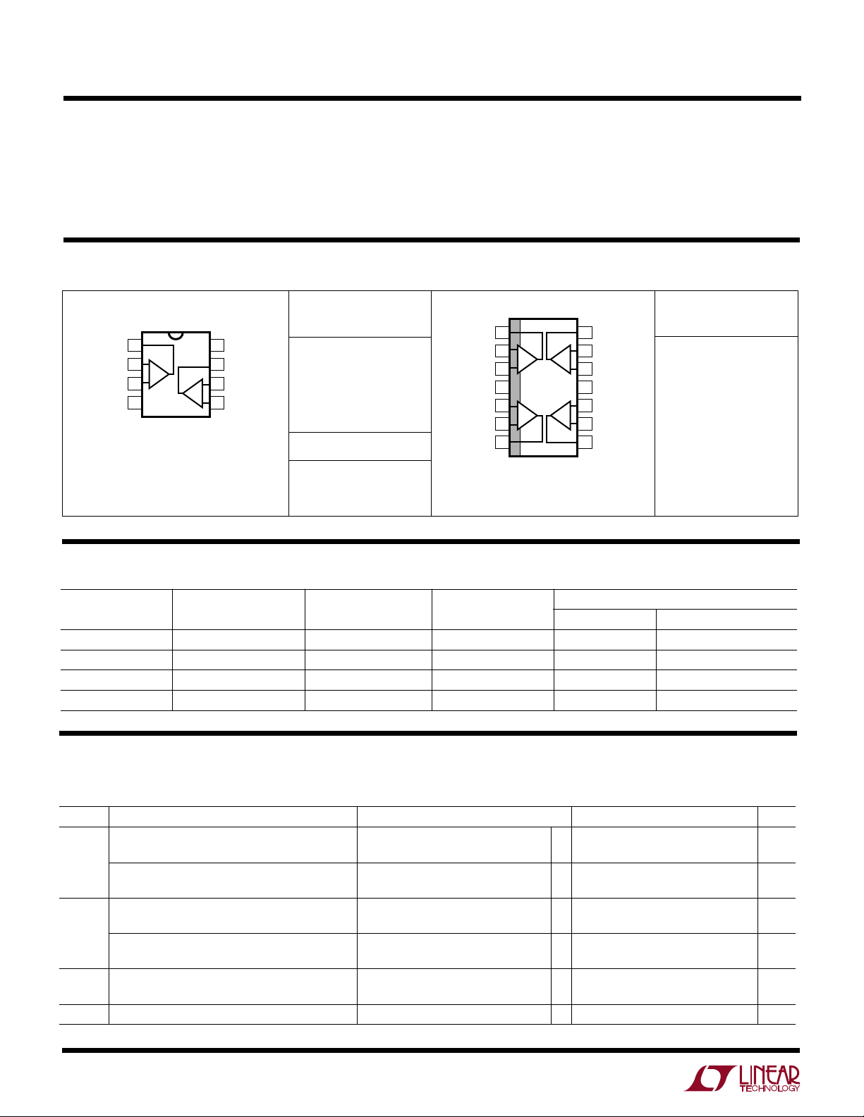
PACKAGE/ORDER INFORMATION
TOP VIEW
OUT A
1
– IN A
2
+IN A
T
T
A
3
–
V
4
N8 PACKAGE
8-LEAD PDIP
S8 PACKAGE
8-LEAD PLASTIC SO
= 150°C, θJA = 130°C/ W (N8)
JMAX
= 150°C, θJA = 190°C/ W (S8)
JMAX
V+
8
7
OUT B
6
–IN B
B
5
+IN B
ORDER PART
NUMBER
LT1366CN8
LT1366CS8
LT1368CN8
LT1368CS8
S8 PART MARKING
1366
1368
Junction Temperature.......................................... 150°C
Storage Temperature Range ................ – 65°C to 150°C
Lead Temperature (Soldering, 10 sec)................. 300°C
ORDER PART
NUMBER
LT1367CS
LT1369CS
1
OUT A
2
–IN A
3
+IN A
+
4
V
5
+IN B
6
–IN B
7
OUT B
14-LEAD PLASTIC SO
T
JMAX
TOP VIEW
14
A
B
S PACKAGE
= 150°C, θJA = 150°C/ W
13
D
12
11
10
C
9
8
OUT D
–IN D
+IN D
–
V
+IN C
– IN C
OUT C
U
AVAILABLE OPTIO S
MAX VOS (25°C)
PRODUCT NUMBER NUMBER OF OP AMPS LOAD CAPACITANCE AT VS = 5V, 0V PLASTIC (N) SURFACE MOUNT(S)
LT1366 2 OpF < CL < 1000pF 475µV LT1366CN8 LT1366CS8
LT1367 4 OpF < CL < 1000pF 800µV LT1367CS
LT1368 2 CL = 0.1µF 475µV LT1368CN8 LT1368CS8
LT1369 4 CL = 0.1µF 800µV LT1369CS
ORDER PART NUMBER
ELECTRICAL CHARACTERISTICS
TA = 25°C, VS = 5V, 0V, VCM = 2.5V, VO = 2.5V, unless otherwise noted.
SYMBOL PARAMETER CONDITIONS MIN TYP MAX UNITS
V
∆V
I
∆I
OS
B
B
Input Offset Voltage (LT1366/LT1368) VCM = V
Input Offset Voltage (LT1367/LT1369) VCM = V
Input Offset Voltage Shift (LT1366/LT1368) VCM = VEE to V
OS
Input Offset Voltage Match (Channel to Channel) V
Input Offset Voltage Shift (LT1367/LT1369) VCM = VEE to V
Input Offset Voltage Match (Channel to Channel) V
Input Bias Current VCM = V
Input Bias Current Shift VCM = VEE to V
V
CM
V
CM
CM
CM
V
CM
CC
= V
EE
CC
= V
EE
= VEE, V
= VEE, V
CC
= V
EE
150 475 µV
150 475 µV
150 800 µV
150 700 µV
CC
(Notes 3, 4) 250 700 µV
CC
CC
(Notes 3, 4) 250 1600 µV
CC
0 10 35 nA
–35 –10 0 nA
CC
150 400 µV
150 650 µV
20 70 nA
2
Page 3
LT1366/LT1367
LT1368/LT1369
ELECTRICAL CHARACTERISTICS
TA = 25°C, VS = 5V, 0V, VCM = 2.5V, VO = 2.5V, unless otherwise noted.
SYMBOL PARAMETER CONDITIONS MIN TYP MAX UNITS
I
OS
∆I
OS
e
n
i
n
C
IN
A
VOL
CMRR Common Mode Rejection Ratio (LT1366/LT1368) VCM = VEE to V
PSRR Power Supply Rejection Ratio VS = 2.0V to 12V, VCM = VO = 0.5V 90 105 dB
V
OL
V
OH
I
SC
I
S
GBW Gain-Bandwidth Product (LT1366/LT1367) AV = 1000 0.4 MHz
t
S
Input Offset Current VCM = V
= V
V
CM
Input Offset Current Shift VCM = V
Input Bias Current Match (Channel to Channel) VCM = V
VCM = V
CC
EE
to V
EE
CC
(Note 3) 0 1 12 nA
CC
(Note 3) 0 1 12 nA
EE
112nA
0.3 12 nA
112nA
Input Noise Voltage Density f = 1kHz 29 nV/√Hz
Input Noise Current Density f = 1kHz 0.07 pA/√Hz
Input Capacitance 12 pF
Large-Signal Voltage Gain VO = 50mV to 4.8V, RL = 10k 250 2000 V/mV
81 90 dB
77 90 dB
CMRR Match (Channel to Channel) V
= VEE to V
CM
Common Mode Rejection Ratio (LT1367/LT1369) VCM = VEE to V
CMRR Match (Channel to Channel) V
PSRR Match (Channel to Channel) (Note 3) V
= VEE to V
CM
= 2.0V to 12V, VCM = VO = 0.5V 84 100 dB
S
CC
(Note 3) 75 90 dB
CC
CC
(Note 3) 71 90 dB
CC
Output Voltage Swing LOW No Load 6 12 mV
I
= 0.5mA 40 70 mV
SINK
= 2.5mA 110 200 mV
I
SINK
Output Voltage Swing HIGH No Load V
= 0.5mA V
I
SOURCE
= 2.5mA V
I
SOURCE
– 0.012 V
CC
– 0.100 V
CC
– 0.250 V
CC
– 0.004 V
CC
– 0.050 V
CC
– 0.150 V
CC
Short-Circuit Current (Note 1) ±15 ±30 mA
Supply Current per Amplifier 340 520 µA
Gain-Bandwidth Product (LT1368/LT1369) A
Settling Time (LT1366/LT1367) AV = 1, V
= 1000 0.16 MHz
V
= 4V to 0.1% 30 µs
STEP
0°C < TA < 70°C, VS = 5V, 0V, VCM = 2.5V, VO = 2.5V, unless otherwise noted.
SYMBOL PARAMETER CONDITIONS MIN TYP MAX UNITS
V
OS
Input Offset Voltage (LT1366/LT1368) VCM = V
= V
V
CM
Input Offset Voltage (LT1367/LT1369) VCM = V
= V
V
CM
CC
EE
CC
EE
● 200 575 µV
● 200 575 µV
● 200 950 µV
● 200 900 µV
VOS TC Input Offset Voltage Drift (Note 2) ● 26µV/°C
∆V
I
B
∆I
B
I
OS
∆IOSInput Offset Current Shift VCM = V
Input Offset Voltage Shift (LT1366/LT1368) VCM = VEE to V
OS
Input Offset Voltage Match (Channel to Channel) V
Input Offset Voltage Shift (LT1367/LT1369) VCM = VEE to V
Input Offset Voltage Match (Channel to Channel) V
Input Bias Current VCM = V
Input Bias Current Shift VCM = VEE to V
Input Offset Current VCM = V
Input Bias Current Match (Channel to Channel) VCM = V
= VEE, V
CM
= VEE, V
CM
CC
VCM = V
EE
CC
= V
V
CM
EE
to V
EE
(Note 3) ● 0215nA
CC
= V
V
CM
(Note 3) ● 0115nA
EE
CC
(Notes 3, 4) ● 250 900 µV
CC
CC
(Notes 3, 4) ● 250 1900 µV
CC
CC
CC
● 200 425 µV
● 200 675 µV
● 0 15 45 nA
● –45 –10 0 nA
● 25 90 nA
● 215nA
● 115nA
● 215nA
3
Page 4
LT1366/LT1367
LT1368/LT1369
ELECTRICAL CHARACTERISTICS
0°C < TA < 70°C, VS = 5V, 0V, VCM = 2.5V, VO = 2.5V, unless otherwise noted.
SYMBOL PARAMETER CONDITIONS MIN TYP MAX UNITS
A
VOL
CMRR Common Mode Rejection Ratio (LT1366/LT1368) VCM = VEE to V
PSRR Power Supply Rejection Ratio VS = 2.3V to 12V, VCM = VO = 0.5V ● 88 105 dB
V
OL
V
OH
I
SC
I
S
Large-Signal Voltage Gain VO = 50mV to 4.8V, RL = 10k ● 250 2000 V/mV
● 80 87 dB
● 77 87 dB
CMRR Match (Channel to Channel) VCM = VEE to V
Common Mode Rejection Ratio (LT1367/LT1369) VCM = VEE to V
CMRR Match (Channel to Channel) V
PSRR Match (Channel to Channel) (Note 3) V
= VEE to V
CM
= 2.3V to 12V, VCM = VO = 0.5V ● 82 100 dB
S
CC
(Note 3) ● 74 87 dB
CC
CC
(Note 3) ● 71 87 dB
CC
Output Voltage Swing LOW No Load ● 914mV
= 0.5mA ● 45 80 mV
I
SINK
= 2.5mA ● 120 230 mV
I
SINK
Output Voltage Swing HIGH No Load ● V
I
= 0.5mA ● V
SOURCE
= 2.5mA ● V
I
SOURCE
– 0.014 V
CC
– 0.110 V
CC
– 0.300 V
CC
– 0.005 V
CC
– 0.055 V
CC
– 0.180 V
CC
Short-Circuit Current (Note 1) ● ±12.5 mA
Supply Current per Amplifier ● 385 540 µA
TA = 25°C, VS = 3V, 0V, VCM = 1.5V, VO = 1.5V, unless otherwise noted.
SYMBOL PARAMETER CONDITIONS MIN TYP MAX UNITS
V
OS
∆V
I
B
∆I
B
I
OS
∆I
OS
A
VOL
CMRR Common Mode Rejection Ratio (LT1366/LT1368) VCM = VEE to V
V
OL
V
OH
I
SC
I
S
Input Offset Voltage (LT1366/LT1368) VCM = V
Input Offset Voltage (LT1367/LT1369) VCM = V
Input Offset Voltage Shift (LT1366/LT1368) VCM = VEE to V
OS
Input Offset Voltage Match (Channel to Channel) V
Input Offset Voltage Shift (LT1367/LT1369) VCM = VEE to V
Input Offset Voltage Match (Channel to Channel) V
Input Bias Current VCM = V
Input Bias Current Shift VCM = VEE to V
Input Offset Current VCM = V
Input Offset Current Shift VCM = V
Input Bias Current Match (Channel to Channel) VCM = V
= V
V
CM
= V
V
CM
= VEE, V
CM
= VEE, V
CM
VCM = V
= V
V
CM
= V
V
CM
CC
EE
CC
EE
CC
(Notes 3, 4) 250 700 µV
CC
CC
(Notes 3, 4) 250 1700 µV
CC
CC
EE
CC
CC
EE
to V
EE
CC
(Note 3) 0 1 12 nA
CC
(Note 3) 0 1 12 nA
EE
0 10 35 nA
–35 –10 0 nA
150 475 µV
150 475 µV
150 850 µV
150 750 µV
150 400 µV
150 650 µV
20 70 nA
1.0 12 nA
0.3 12 nA
112nA
Large-Signal Voltage Gain VO = 50mV to 2.8V, RL = 10k 250 1500 V/mV
77 86 dB
73 86 dB
CMRR Match (Channel to Channel) V
= VEE to V
CM
Common Mode Rejection Ratio (LT1367/LT1369) VCM = VEE to V
CMRR Match (Channel to Channel) VCM = VEE to V
CC
(Note 3) 71 86 dB
CC
CC
(Note 3) 67 86 dB
CC
Output Voltage Swing LOW No Load 6 12 mV
= 0.5mA 40 70 mV
I
SINK
= 2.5mA 110 200 mV
I
SINK
Output Voltage Swing HIGH No Load V
= 0.5mA V
I
SOURCE
= 2.5mA V
I
SOURCE
– 0.012 V
CC
– 0.100 V
CC
– 0.250 V
CC
– 0.004 V
CC
– 0.050 V
CC
– 0.150 V
CC
Short-Circuit Current (Note 1) ±10 ±20 mA
Supply Current per Amplifier 330 500 µA
4
Page 5
LT1366/LT1367
LT1368/LT1369
ELECTRICAL CHARACTERISTICS
0°C < TA < 70°C, VS = 3V, 0V, VCM = 1.5V, VO = 1.5V, unless otherwise noted.
SYMBOL PARAMETER CONDITIONS MIN TYP MAX UNITS
V
OS
∆V
VOS TC Input Offset Voltage Drift (Note 2) ● 26µV/°C
I
B
∆I
B
I
OS
∆IOSInput Offset Current Shift VCM = V
A
VOL
CMRR Common Mode Rejection Ratio (LT1366/LT1368) VCM = VEE to V
V
OL
V
OH
I
SC
I
S
Input Offset Voltage (LT1366/LT1368) VCM = V
Input Offset Voltage (LT1367/LT1369) VCM = V
Input Offset Voltage Shift (LT1366/LT1368) VCM = VEE to V
OS
Input Offset Voltage Match (Channel to Channel) V
Input Offset Voltage Shift (LT1367/LT1369) VCM = VEE to V
Input Offset Voltage Match (Channel to Channel) V
Input Bias Current VCM = V
Input Bias Current Shift VCM = VEE to V
Input Offset Current VCM = V
Input Bias Current Match (Channel to Channel) VCM = V
CC
= V
V
CM
EE
CC
VCM = V
EE
= VEE, V
CM
= VEE, V
CM
CC
= V
V
CM
EE
CC
V
= V
CM
EE
to V
EE
(Note 3) ● 0215nA
CC
= V
V
CM
(Note 3) ● 0115nA
EE
CC
(Notes 3, 4) ● 250 900 µV
CC
CC
(Notes 3, 4) ● 250 1900 µV
CC
CC
CC
● 200 575 µV
● 200 575 µV
● 200 950 µV
● 200 900 µV
● 200 425 µV
● 200 675 µV
● 0 15 45 nA
● –45 –10 0 nA
● 25 90 nA
● 215nA
● 115nA
● 215nA
Large-Signal Voltage Gain VO = 50mV to 2.8V, RL = 10k ● 150 1500 V/mV
● 76 83 dB
● 72 83 dB
CMRR Match (Channel to Channel) V
= VEE to V
CM
Common Mode Rejection Ratio (LT1367 /LT1369) VCM = VEE to V
CMRR Match (Channel to Channel) V
= VEE to V
CM
CC
(Note 3) ● 70 83 dB
CC
CC
(Note 3) ● 66 83 dB
CC
Output Voltage Swing LOW No Load ● 914mV
= 0.5mA ● 45 80 mV
I
SINK
I
= 2.5mA ● 120 230 mV
SINK
Output Voltage Swing HIGH No Load ● V
= 0.5mA ● V
I
SOURCE
= 2.5mA ● V
I
SOURCE
– 0.014 V
CC
– 0.110 V
CC
– 0.300 V
CC
– 0.005 V
CC
– 0.055 V
CC
– 0.180 V
CC
Short-Circuit Current (Note 1) ● ±10 mA
Supply Current per Amplifier ● 375 520 µA
5
Page 6
LT1366/LT1367
LT1368/LT1369
ELECTRICAL CHARACTERISTICS
TA = 25°C, VS = ±15V, VCM = 0V, VO = 0V, unless otherwise noted.
SYMBOL PARAMETER CONDITIONS MIN TYP MAX UNITS
V
OS
∆V
I
B
∆I
B
I
OS
∆I
OS
C
IN
A
VOL
SR Slew Rate (LT1366/LT1367) AV = –1, RL = Open, VO = ±10V, 0.13 V/µs
CMRR Common Mode Rejection Ratio (LT1366/LT1368) VCM = VEE to V
PSRR Power Supply Rejection Ratio VS = ±5V to ±15V 90 110 dB
V
OL
V
OH
I
SC
I
S
Input Offset Voltage (LT1366/LT1368) VCM = V
Input Offset Voltage (LT1367/LT1369) VCM = V
Input Offset Voltage Shift (LT1366/LT1368) VCM = VEE to V
OS
Input Offset Voltage Match (Channel to Channel) V
Input Offset Voltage Shift (LT1367/LT1369) VCM = VEE to V
Input Offset Voltage Match (Channel to Channel) V
Input Bias Current VCM = V
Input Bias Current Shift VCM = VEE to V
Input Offset Current VCM = V
Input Offset Current Shift VCM = V
Input Bias Current Match (Channel to Channel) VCM = V
V
CM
V
CM
CM
CM
V
CM
V
CM
V
CM
CC
= V
EE
CC
= V
EE
= VEE, V
= VEE, V
= V
= V
= V
CC
(Notes 3, 4) 300 1300 µV
CC
CC
(Notes 3, 4) 300 2000 µV
CC
CC
EE
CC
CC
EE
to V
EE
CC
(Note 3) 0 1 12 nA
CC
(Note 3) 0 1 12 nA
EE
0 10 35 nA
–35 –10 0 nA
200 700 µV
200 700 µV
200 1000 µV
200 900 µV
150 500 µV
150 650 µV
20 70 nA
1.0 12 nA
0.3 12 nA
112nA
Input Capacitance 7.1 pF
Large-Signal Voltage Gain VO = –14.7V to 14.7V, RL = 10k 1000 10000 V/mV
= –10V to 10V, RL = 2k 500 10000 V/mV
V
O
Channel Separation VO = –10V to 10V, RL = 2k 120 135 dB
Measured at V
= ±5V
O
Slew Rate (LT1368/LT1369) AV = –1, RL = Open, VO = ±10V, 0.065 V/µs
Measured at V
CMRR Match (Channel to Channel) V
= VEE to V
CM
Common Mode Rejection Ratio (LT1367/LT1369) VCM = VEE to V
CMRR Match (Channel to Channel) V
= VEE to V
CM
= ±5V
O
CC
(Note 3) 89 106 dB
CC
CC
(Note 3) 87 106 dB
CC
95 106 dB
93 106 dB
PSRR Match (Channel to Channel) VS = ±5V to ±15V (Note 3) 84 105 dB
Output Voltage Swing LOW No Load V
= 0.5mA V
I
SINK
= 10mA V
I
SINK
Output Voltage Swing HIGH No Load V
= 0.5mA V
I
SOURCE
= 10mA V
I
SOURCE
– 0.012 V
CC
– 0.100 V
CC
– 0.800 V
CC
+ 0.006 V
EE
+ 0.040 V
EE
+ 0.240 V
EE
– 0.004 V
CC
– 0.050 V
CC
– 0.400 V
CC
EE
EE
EE
Short-Circuit Current (Note 1) ±30 ±75 mA
Supply Current per Amplifier 370 550 µA
+ 0.012 V
+ 0.070 V
+ 0.500 V
6
Page 7

LT1366/LT1367
LT1368/LT1369
ELECTRICAL CHARACTERISTICS
0°C < TA < 70°C, VS = ±15V, VCM = 0V, VO = 0V, unless otherwise noted.
SYMBOL PARAMETER CONDITIONS MIN TYP MAX UNITS
V
OS
∆V
VOS TC Input Offset Voltage Drift (Note 2) ● 28µV/°C
I
B
∆I
B
I
OS
∆IOSInput Offset Current Shift VCM = V
A
VOL
CMRR Common Mode Rejection Ratio (LT1366/LT1368) VCM = VEE to V
PSRR Power Supply Rejection Ratio VS = ±5V to ±15V ● 80 105 dB
V
OL
V
OH
I
SC
I
S
The ● denotes specifications that apply over the full operating temperature
range.
Note 1: Applies to short circuits to ground for all split supplies and for
single supplies less than 20V. Short circuits to either supply for supplies
greater than 20V total may permanently damage the part. A heat sink may
be required to keep the junction temperature below the absolute maximum
rating when the output is shorted indefinitely.
Input Offset Voltage (LT1366/LT1368) VCM = V
Input Offset Voltage (LT1367/LT1369) VCM = V
Input Offset Voltage Shift (LT1366/LT1368) VCM = VEE to V
OS
Input Offset Voltage Match (Channel to Channel) V
Input Offset Voltage Shift (LT1367/LT1369) VCM = VEE to V
Input Offset Voltage Match (Channel to Channel) V
Input Bias Current VCM = V
Input Bias Current Shift VCM = VEE to V
Input Offset Current VCM = V
Input Bias Current Match (Channel to Channel) VCM = V
CC
= V
V
CM
EE
CC
VCM = V
EE
= VEE, V
CM
= VEE, V
CM
CC
= V
V
CM
EE
CC
V
= V
CM
EE
to V
EE
(Note 3) ● 0215nA
CC
= V
V
CM
(Note 3) ● 0115nA
EE
CC
(Notes 3, 4) ● 300 1500 µV
CC
CC
(Notes 3, 4) ● 300 2300 µV
CC
CC
CC
● 250 850 µV
● 250 850 µV
● 250 1150 µV
● 250 1000 µV
● 200 525 µV
● 200 750 µV
● 0 15 45 nA
● –45 –10 0 nA
● 25 90 nA
● 215nA
● 115nA
● 215nA
Large-Signal Voltage Gain VO = –14.7V to 14.7V, RL = 10k ● 750 6000 V/mV
= –10V to 10V, RL = 2k ● 500 6000 V/mV
V
O
Channel Separation VO = –10V to 10V, RL = 2k ● 110 135 dB
● 95 103 dB
● 92 103 dB
CMRR Match (Channel to Channel) V
= VEE to V
CM
Common Mode Rejection Ratio (LT1367/LT1369) VCM = VEE to V
CMRR Match (Channel to Channel) VCM = VEE to V
PSRR Match (Channel to Channel) V
= ±5V to ±15V (Note 3) ● 75 100 dB
S
CC
(Note 3) ● 89 103 dB
CC
CC
(Note 3) ● 86 103 dB
CC
Output Voltage Swing LOW No Load ● VEE + 0.009 VEE + 0.014 V
= 0.5mA ● VEE + 0.045 VEE + 0.080 V
I
SINK
= 10mA ● VEE + 0.300 VEE + 0.600 V
I
SINK
Output Voltage Swing HIGH No Load ● V
= 0.5mA ● V
I
SOURCE
= 10mA ● V
I
SOURCE
– 0.014 V
CC
– 0.11 V
CC
– 0.95 V
CC
– 0.005 V
CC
– 0.055 V
CC
– 0.500 V
CC
Short-Circuit Current (Note 1) ● ±30 mA
Supply Current per Amplifier ● 415 575 µA
Note 2: This parameter is not 100% tested.
Note 3: Matching parameters are the difference between amplifiers A and
D and between B and C on the LT1367/LT1369; between the two amplifiers
on the LT1366/LT1368.
Note 4: Input offset voltage match is the difference in offset voltage
between amplifiers measured at both V
= VEE and VCM = VCC.
CM
7
Page 8

LT1366/LT1367
LOAD CURRENT (mA)
0.001
SATURATION VOLTAGE (mV)
100
1000
0.01 0.1 1 10
LT1366 TPC09
10
1
TA = 85°C
TA = –55°C
TA = 25°C
INPUT OFFSET VOLTAGE (µV)
–350
20
25
30
–150 50
LT1366 TPC01
15
10
–250
–50 150 350250
5
0
PERCENT OF UNITS (%)
N-PACKAGE
V
S
= 5V, 0V
V
CM
= 0V TO 5V
COMMON MODE VOLTAGE (V)
INPUT BIAS CURRENT (nA)
10
20
LT1366 TPC06
0
–10
–20
0
2
4
5
15
–5
–15
56
–1–2
1
3
VS = 5V, 0V
TA = –55°C
TA = 125°C
TA = 25°C
LT1368/LT1369
W
U
TYPICAL PERFORMANCE CHARACTERISTICS
(The data presented here applies to the LT1366/LT1367/LT1368/LT1369 unless otherwise noted.)
PNP Stage V
Distribution
OS
(LT1366/LT1368)
30
N-PACKAGE
= 5V, 0V
V
S
25
= 0V
V
CM
20
15
10
PERCENT OF UNITS (%)
5
0
–350
–250
–50 150 350250
–150 50
INPUT OFFSET VOLTAGE (µV)
Supply Current vs Temperature
500
400
300
200
100
SUPPLY CURRENT PER AMPLIFIER (µA)
0
–20–35 –5 25 55 85
–50
VS = ±15V
10
TEMPERATURE (°C)
VS = 5V, 0V
40
LT1366 TPC03
70
LT1366 TPC04
100
NPN Stage V
Distribution
OS
(LT1366/LT1368)
30
N-PACKAGE
= 5V, 0V
V
S
25
= 5V
V
CM
20
15
10
PERCENT OF UNITS (%)
5
0
–350
–250
–50 150 350250
–150 50
INPUT OFFSET VOLTAGE (µV)
Supply Current vs Supply Voltage
600
500
400
300
200
100
SUPPLY CURRENT PER AMPLIFIER (µA)
0
0
TA = 125°C
TA = 25°C
TA = –55°C
412
8
TOTAL SUPPLY VOLTAGE (V)
20 36
16
∆VOS-Shift Between PNP and NPN
Stages (LT1366/LT1368)
LT1366 TPC02
Input Bias Current vs
Common Mode Voltage
28
32
24
LT1366 TPC05
50
40
30
20
10
0
–10
–20
INPUT BIAS CURRENT (nA)
–30
–40
–50
–50
8
Input Bias Current
vs Temperature
VS = 5V, 0V, VCM = 5V
VS = ±15V, VCM = 15V
VS = 5V, 0V, VCM = 0V
VS = ±15V, VCM = –15V
–20–35 –5 25 55 85
10
TEMPERATURE (°C)
40
70
LT1366 TPC07
100
Output Saturation Voltage vs
Load Current (Output HIGH)
1000
100
10
SATURATION VOLTAGE (mV)
1
0.001
0.01 0.1 1 10
LOAD CURRENT (mA)
Output Saturation Voltage vs
Load Current (Output LOW)
TA = 85°C
TA = 25°C
TA = –55°C
LT1366 TPC08
Page 9

W
FREQUENCY (Hz)
–20
VOLTAGE GAIN (dB)
0
10
30
50
1k 100k 1M 10M
LT1366 TPC15
–40
–50
10k
20
–10
–30
40
0
40
60
100
140
–40
–60
80
20
–20
120
PHASE SHIFT (DEG)
GAIN
PHASE
VS = ±2.5V
C
L
= 0.1µF
FREQUENCY (Hz)
1
40
50
60
70
10 100 1000
LT1366 TPC12
30
20
0
10
VS = 5V, 0V
VCM = 4V
VCM = 2.5V
NOISE VOLTAGE nV/√Hz
U
TYPICAL PERFORMANCE CHARACTERISTICS
(The data presented here applies to the LT1366/LT1367/LT1368/LT1369 unless otherwise noted.)
0.1Hz to 10Hz
Minimum Supply Voltage
200
150
TA = 70°C
Output Voltage Noise
VS = ±2.5V
= 0V
V
CM
LT1366/LT1367
LT1368/LT1369
Noise Voltage Spectrum
100
50
0
CHANGE IN OFFSET VOLTAGE (µV)
NONFUNCTIONAL
1
TA = 85°C
2
TOTAL SUPPLY VOLTAGE (V)
Noise Current Spectrum
0.8
0.7
0.6
0.5
CURRENT NOISE (pA/√Hz)
0.4
0.3
0.2
0.1
0
1
VCM = 2.5V
VCM = 4V
10 100 1000
FREQUENCY (Hz)
TA = 25°C
TA = –55°C
3
5
4
LT1366 TPC10
VS = 5V, 0V
LT1366 TPC13
70
60
50
40
30
20
10
VOLTAGE GAIN (dB)
0
–10
–20
–30
OUTPUT VOLTAGE (200nV/DIV)
TIME (1s/DIV)
LT1366 TPC11
Gain and Phase Shift vs
Frequency (LT1366/LT1367)
VS = ±2.5V
PHASE
GAIN
1k 100k 1M 10M
10k
FREQUENCY (Hz)
LT1366 TPC14
140
120
100
PHASE SHIFT (DEG)
80
60
40
20
0
–20
–40
–60
Gain and Phase Shift vs
Frequency (LT1368/LT1369)
CMRR vs Frequency
(LT1366 and LT1367)
120
110
100
90
80
70
60
50
40
30
COMMON-MODE REJECTION RATIO (dB)
20
1k 100k 1M
10k
FREQUENCY (Hz)
VS = ±2.5V
LT1366 TPC16
PSRR vs Frequency
(LT1366/LT1367)
120
100
80
60
40
20
POWER SUPPLY REJECTION RATIO (dB)
NEGATIVE SUPPLY
0
1k 100k 1M
POSITIVE SUPPLY
10k
FREQUENCY (Hz)
VS = ±2.5V
LT1366 TPC17
PSRR vs Frequency
(LT1368/LT1369)
120
100
80
60
40
20
POWER SUPPLY REJECTION RATIO (dB)
NEGATIVE SUPPLY
0
1k 100k 1M
POSITIVE SUPPLY
10k
FREQUENCY (Hz)
VS = ±2.5V
LT1366 TPC18
9
Page 10

LT1366/LT1367
LOAD CURRENT (mA)
–10
0
OVERSHOOT (%)
10
20
30
40
50
60
–5 0 5 10
LT1366 TPC24
CL = 0.22µF
VS = ±15V
A
V
= 1
CL = 0.1µF
CL = 0.047µF
V
IN(P-P)
(V)
0.01
THD + NOISE (%)
0.1
1
10
0234
0.001
1
5
LT1366 TPC27
f = 1kHz
R
L
= 10k
(ALL CURVES)
V
S
= ±1.5V
A
V
= 1
V
S
= ±1.5V
A
V
= –1
VS = ±2.5V
A
V
= 1
VS = ±2.5V
A
V
= –1
LT1368/LT1369
W
U
TYPICAL PERFORMANCE CHARACTERISTICS
(The data presented here applies to the LT1366/LT1367/LT1368/LT1369 unless otherwise noted.)
Gain-Bandwidth and Phase
Margin vs Supply Voltage
(LT1366/LT1367)
500
450
400
350
300
250
200
FREQUENCY (kHz)
150
100
50
0
0
5
GBW
PHASE MARGIN
15 20
10
SUPPLY VOLTAGE (V)
25
30
LT1366 TPC19
60
54
48
42
36
30
24
18
12
6
0
PHASE MARGIN (DEG)
Channel Separation vs Frequency
–50
VS = ±15V
–60
–70
–80
–90
–100
–110
–120
CHANNEL SEPARATION (dB)
–130
–140
–150
= ±1V
V
OUT
= 2k
R
L
10 1k 10k
P-P
LT1368/LT1369
100
FREQUENCY (Hz)
LT1366/LT1367
LT1366 TPC20
20
15
10
5
0
–5
INPUT VOLTAGE (µV)
–10
–15
–20
–20
Open-Loop Gain
–15
–10
–5
OUTPUT VOLTAGE (V)
RL = 2k
RL = 10k
0
5
VS = ±15V
10
15
LT1366 TPC21
20
Capacitive Load Handling
(LT1366/LT1367)
80
VS = 5V, 0V
70
60
50
40
30
OVERSHOOT (%)
20
10
0
10 1k 10k 100k
AV = 1
100
CAPACITIVE LOAD (pF)
Slew Rate vs Supply Voltage Warm-Up Drift vs Time
0.20
AV = –1
0.18
0.16
0.14
SLEW RATE (V/µs)
0.12
0.10
0
10
8
412
TOTAL SUPPLY VOLTAGE (V)
20 36
16
AV = 5
24
AV = 10
LT1366 TPC22
28
LT1366 TPC25
Overshoot vs Load Current
(LT1368/LT1369)
60
VS = ±2.5V
= 1
A
V
50
40
CL = 0.047µF
30
OVERSHOOT (%)
20
10
0
–10
–5 0 5 10
LOAD CURRENT (mA)
CL = 0.22µF
CL = 0.1µF
LT1366 TPC23
Overshoot vs Load Current
(LT1368/LT1369)
THD + Noise vs
Peak-to-Peak Voltage
80
60
40
20
0
–20
–40
CHANGE IN OFFSET VOLTAGE (µV)
–60
32
–80
15
0
S8 PACKAGE
= ±15V
V
S
S8 PACKAGE
= ±2.5V
V
S
N8 PACKAGE
= ±2.5V
V
S
N8 PACKAGE
= ±15V
V
S
30
45
TIME AFTER POWER-UP (SEC)
90
75
60
105
120
135
LT1366 TPC26
150
Page 11

W
U
TYPICAL PERFORMANCE CHARACTERISTICS
(The data presented here applies to the LT1366/LT1367/LT1368/LT1369 unless otherwise noted.)
LT1366/LT1367
LT1368/LT1369
Large-Signal Response
THD + Noise vs Frequency
1
VS = ±1.5V
= 2V
IN
= 10k
L
P-P
0.1 1 10
FREQUENCY (kHz)
V
R
0.1
THD + NOISE (%)
0.01
0.001
0.01
AV = 1
= –1
A
V
LT1366 TPC28
U
WUU
(LT1366/LT1367)
0V
5V/DIV
VS = ±15V 100µs/DIV
UNITY-GAIN
APPLICATIONS INFORMATION
Rail-to-Rail Operation
The LT1366 family differs from conventional op amps in
the design of both the input and output stages. Figure 1
shows a simplified schematic of the amplifier. The input
stage consists of two differential amplifiers, a PNP stage
Q1/Q2 and an NPN stage Q3/Q4, which are active over
Small-Signal Response
(LT1366/LT1367)
5mV/DIV
LT1366 TPC29
VS = ±15V 2µs/DIV
UNITY-GAIN
LT1366 TPC30
different portions of the input common mode range.
Lateral devices are used in both input stages, eliminating
the need for clamps across the input pins. Each input stage
is trimmed for offset voltage. A complementary output
configuration (Q23 through Q26) is employed to create an
output stage with rail-to-rail swing. The amplifier is fabri-
– 300mV
+
V
D7
Q24
Q23
–
V
C1
C2
V
Q25
OUT
+
Q26
D8
LT1366 FO1
Q17
Q19
Q20
D6
Q21
–
V
+
V
Q22
D5D4
I1
Q5
–
V
+
IN
–
IN
Q12
+
V
–
V
Q3 Q4
Q6
Q1 Q2
D1
D3
D2
Q10
Q11
–
V
+
V
Q7
Q8
C
C
Q15
Q14
Q9
Q13
D7
Q16
+
V
Q18
Figure 1. LT1366 Simplified Schematic Diagram
11
Page 12

LT1366/LT1367
COMMON MODE VOLTAGE RELATIVE TO
POSITIVE SUPPLY (mV)
–500
0
INPUT BIAS CURRENT (nA)
20
40
60
80
–300 –100 V
S
LT1366 F02
100
100
110
90
70
50
30
10
300 500
T = –55°C
T = 25°C
T = 85°C
T = 70°C
MEASURED AS A
FOLLOWER
–
+
LT1368/LT1369
U
WUU
APPLICATIONS INFORMATION
cated on Linear Technology’s proprietary complementary
bipolar process, which ensures very similar DC and AC
characteristics for the output devices Q24 and Q26.
A simple comparator Q5 steers current from current
source I1 between the two input stages. When the input
common mode voltage VCM is near the negative supply,
Q5 is reverse biased, and I1 becomes the tail current for
the PNP differential pair Q1/Q2. At the other extreme,
when VCM is within about 1.3V from the positive supply,
Q5 diverts I1 to the current mirror D3/Q6, which furnishes
the tail current for the NPN differential pair Q3/Q4.
The collector currents of the two input pairs are combined
in the second stage, consisting of Q7 through Q11. Most
of the voltage gain in the amplifier is contained in this
stage. Differential amplifier Q14/Q15 buffers the output of
the second stage, converting the output voltage to differential currents. The differential currents pass through
current mirrors D4/Q17 and D5/Q16, and are converted to
differential voltages by Q18 and Q19. These voltages are
also buffered and applied to the output Darlington pairs
Q23/Q24 and Q25/Q26. Capacitors C1 and C2 form local
feedback loops around the output devices, lowering the
output impedance at high frequencies.
When overdriven, the amplifier draws input current that
exceeds the normal input bias current. Figures 2 and 3
show some typical overdrive currents as a function of
input voltage. The input current must be less than 1mA of
positive overdrive or less than 7mA of negative overdrive,
for the phase reversal protection to work properly. When
the amplifier is severely overdriven, an external resistor
should be used to limit the overdrive current. In addition
to overdrive protection, the amplifier is protected against
ESD strokes up to 4kV on all pins.
Input Offset Voltage
Since the amplifier has two input stages, the input offset
voltage changes depending upon which stage is active.
The input offsets are random, but bounded voltages.
When the amplifier switches between stages, offset voltages may go up, down, or remain flat; but will not exceed
the guaranteed limits. This behavior is illustrated in three
distribution plots of input offset voltage in the Typical
Performance Characteristics section.
Overdrive Protection
Two circuits prevent the output from reversing polarity
when the input voltage exceeds the common mode range.
When the noninverting input exceeds the positive supply
by approximately 300mV, the clamp transistor Q12 (Figure 1) turns on, pulling the output of the second stage low,
which forces the output high. For inputs below the negative supply, diodes D1 and D2 turn on, overcoming the
saturation of the input pair Q1/Q2.
12
Figure 2. Input Bias Current vs Common Mode Voltage
0
MEASURED AS A FOLLOWER
–10
+
–20
–30
–40
–50
–60
–70
–80
INPUT BIAS CURRENT (nA)
–90
–100
–110
–
T = –55°C T = 25°C
T = 85°C
–800
–600 –400
COMMON MODE VOLTAGE RELATIVE TO
NEGATIVE SUPPLY (mV)
–200
T = 70°C
V
S
200
LT1366 F03
Figure 3. Input Bias Current vs Common Mode Voltage
Page 13

LT1366/LT1367
CS/SHDN
CH0
CH1
GND
V
CC
(REF)
CLK
D
OUT
D
IN
LTC1288
–
+
–
+
TO µP
1µF
0.1µF
0.1µF
0.1µF
V
CC
V
0
V
1
1/2 LT1368
1/2 LT1368
LT1366 FO5
LT1368/LT1369
U
WUU
APPLICATIONS INFORMATION
Improved Supply Rejection in the LT1368/LT1369
The LT1368/LT1369 are variations of the LT1366/LT1367
offering greater supply rejection and lower high frequency
output impedance. The LT1368/LT1369 require a 0.1µF
load capacitance for compensation. The output capacitance forms a filter, which reduces pickup from the supply
and lowers the output impedance. This additional filtering
is helpful in mixed analog/digital systems with common
supplies, or systems employing switching supplies. Filtering also reduces high frequency noise, which may be
beneficial when driving A/D converters.
+
V
(AC)
100mV/DIV
Figure 4 shows the outputs of the LT1366/LT1368 perturbed by a 200mV
50kHz square wave added to the
P-P
positive supply. The LT1368’s power supply rejection is
about ten times greater than that of the LT1366 at 50kHz.
Note the 5-to-1 scale change in the output voltage traces.
The tolerance of the external compensation capacitor is
not critical. The plots of Overshoot vs Load Current in the
Typical Performance Characteristics section illustrate the
effect of a capacitive load.
+
V
(AC)
100mV/DIV
V
OUT
100mV/DIV
2µs/DIV LT1366 F04a
Figure 4a. LT1366 Power Supply Rejection Test
U
TYPICAL APPLICATIONS
Buffering A/D Converters
Figure 5 shows the LT1368 driving an LTC®1288
2-channel micropower A/D Converter (ADC). The LTC1288
can accommodate voltage references and input signals
equal to the supply rails. The sampling nature of this ADC
eliminates the need for an external sample-and-hold, but
may call for a drive amplifier because of the ADC’s 12µs
settling requirement. The LT1368’s rail-to-rail operation
and low input offset voltage make it well-suited for low
power, low frequency A/D applications. Either the LT1366
or LT1368 could be used for this application. However, for
low frequencies (f < 1kHz) the LT1368 provides better
supply rejection.
V
OUT
20mV/DIV
2µs/DIV LT1366 F04b
Figure 4b. LT1368 Power Supply Rejection Test
Figure 5. 2-Channel Low Power A/D Converter
13
Page 14

LT1366/LT1367
LT1368/LT1369
U
TYPICAL APPLICATIONS
Precision Low Dropout Regulator
Microprocessors and complex digital circuits frequently
specify tight control of power supply characteristics. The
circuit shown in Figure 6 provides a precise 3.6V, 1A
output from a minimum 3.8V input voltage. The circuit's
nominal operating voltage is 4.75V ±5%. The voltage
reference and resistor ratios determine output voltage
accuracy, while the LT1366’s high gain enforces 0.2% line
and load regulation. Quiescent current is about 1mA and
does not change appreciably with supply or load. All
components are available in surface mount packages.
The regulator’s main loop consists of A1 and a logic level
FET, Q1. The output is fed back to the op amp’s positive
input because of the phase inversion through Q1. The
regulator’s frequency response is limited by Q1’s roll-off
and the phase lead introduced by the output capacitor’s
effective series resistance (ESR). Two pole-zero networks
compensate for these effects. The pole formed with R5
and C2 rolls off the gain set with the feedback network,
while the pole formed with R7 and C3 rolls off A1’s gain
directly, which is the dominant influence on settling time.
The zeros formed with R6 and C2, and R8 and C3 provide
phase boost near the unity-gain crossover, which in-
creases the regulator’s phase margin. Although not directly part of the compensation, R9 decouples the op
amp’s output from Q1’s large gate capacitance.
A second loop provides a foldback current limit. A2
compares the sense voltage across R1 with 50mV referenced to the positive rail. When the sense voltage exceeds
the reference, A2’s output drives Q1’s gate positive via A1.
In current limit, the output voltage collapses and the
current limit LED (D1) turns on causing about 30mV to
drop across R3. A2 regulates Q1’s drain current so that the
deficit between the 50mV reference and the voltage across
R3 is made up across the sense resistor. The reduced
sense voltage is 20mV, which sets the current limit to
about 400mA. As the supply voltage increases, the voltage
across R3 increases, and the current limit folds back to a
lower level. The current limit loop deactivates when the
load current drops below the regulated output current.
When the supply turns on rapidly, C1 bypasses the fold
back circuit allowing the regulator to start-up into a heavy
load.
Q1 does not require a heat sink. When mounted on a type
FR4 PC board, Q1 has a thermal resistance of 50°C/W. At
1.4W worst case dissipation, Q1 can operate up to 80°C.
C4
1µF
1% METAL FILM
*
SET R
**
MIN
R8
10k
R7
13k
2k
–
A1
1/2 LT1366
+
LT1004-1.2
BASED ON LOAD CHARACTERISTICS
R5*
20k
4.75V TO 3.6V LDO AT 1A
Figure 6. Precision 3.6V, 1A Low Dropout Regulator
R6
6.2k
C3
6.8nF
38.5k*
C2
6.8nF
R9
100Ω
R
1k
MIN
= 4.75V ±5%
V
IN
+
**
R1
0.05Ω
Q1
Si9433DY
1.5k
C
LOAD
10µF
R3
20Ω
V
AT 1A
OUT
C1
10µF
+
= 3.6V
+
+
R2
50mV
2k
–
R4
10k
D1
Q2
2N3904
23.2k
C5
47µF
–
A2
1/2 LT1366
+
0.1µF
D2
1N4148
5k
LT1366 F06
14
Page 15

U
TYPICAL APPLICATIONS
LT1366/LT1367
LT1368/LT1369
High-Side Current Source
The wide-compliance current source shown in Figure 7
takes advantage of the LT1366’s ability to measure small
signals near the positive supply rail. The LT1366 adjusts
Q1’s gate voltage to force the voltage across the sense
resistor (R
) to equal the voltage from the supply to
SENSE
the potentiometer’s wiper. A rail-to-rail op amp is needed
because the voltage across the sense resistor must drop
to zero when the divided reference voltage is set to zero.
Q2 acts as a constant current sink to minimize error in the
reference voltage when the supply voltage varies.
LT1004-1.2
V
CC
–
1/2 LT1366
R
10k
P
40k
Q2
2N4340
+
5V < VCC < 30V
0A < I
LOAD
0mA < I
Figure 7. High-Side Current Source
R
SENSE
0.2Ω
1k
0.0033µF
100Ω
I
LOAD
< 1A AT VCC = 5V
< 160mA AT VCC = 30V
LOAD
Q1
MTP23P06
LT1366 F07
The circuit can operate over a wide supply range
(5V < VCC < 30V). At low input voltage, circuit operation is
limited by the MOSFET’s gate drive requirements. At high
input voltage, circuit operation is limited by the LT1366’s
absolute maximum ratings and the output power requirements.
The circuit delivers 1A at 200mV of sense voltage. With a
5V input supply, the power dissipation is 5W. For operation at 70°C ambient temperature, the MOSFET’s heat sink
must have a thermal resistance of:
θHS = θ
JA SYSTEM
– θ
JC FET
= (125°C – 70°C)/5W – 1.25°C/W
= 11°C/W –1.25°C/W
= 9.75°C/W
which is easily achievable with a small heat sink. Input
voltages greater than 5V require the use of a larger heat
sink or a reduction of the output current.
The circuit’s supply regulation is about 0.03%/V. The
output impedance is equal to the MOSFET’s output impedance multiplied by the op amp’s open-loop gain. Degradations in current-source compliance occur when the voltage across the MOSFET’s on-resistance and the sense
resistor drops below the voltage required to maintain the
desired output current. This condition occurs when
[V
CC
– V
OUT
] < [I
LOAD
• (R
SENSE
+ RON)].
Single Supply, 1kHz, 4th Order Butterworth Filter
An LT1367 is used in Figure 8 to form a 4th order
Butterworth filter. The filter is a simplified state variable
architecture consisting of two cascaded 2nd order sections. Each section uses the 360 degree phase shift around
R1*
29.5k
V
IN
3.3V
*1% RESISTORS
C1
–
A1
1/4 LT1367
+
10k
10,000pF
29.5k*
10k
R2*
8.6k
1µF
10,000pF
–
A2
1/4 LT1367
+
C2
10,000pF
10,000pF
11.8k*
–
A3
1/4 LT1367
+
21.5k*
–
A4
1/4 LT1367
+
11.8k*
Figure 8. 4-Pole 1kHz, 3.3V Single Supply, State Variable Filter Using the LT1367
V
OUT
LT1366 F08
15
Page 16

LT1366/LT1367
LT1368/LT1369
U
TYPICAL APPLICATIONS
the 2 op amp loop to create a negative summing junction
at A1’s positive input1. The circuit has low sensitivities for
center frequency and Q, which are set with the following
equations:
2
ω
= 1/(R1 • C1 • R2 • C2)
0
where,
10k
+
V
2
–
1/2 LT1366
3
V
IN
+
1
SIGNAL AMP
V
OUT
R1 = 1/(ω0 • Q • C1) and R2 = Q/(ω0 • C2).
The DC bias applied to A2 and A4, half supply, is not
needed when split supplies are available. The circuit
swings rail-to-rail in the passband making it an excellent
anti-aliasing filter for ADCs. The amplitude response is flat
to 1kHz then rolls off at 80dB/decade.
1
James Hahn, “State Variable Filter Trims Predecessor’s Component Count,”
21, 1982.
0
–20
–40
GAIN (dB)
–60
–80
100
GAIN
FREQUENCY (Hz)
PHASE
1k 10k
1366 F09
Electronics,
180
144
108
72
36
0
–36
–72
–108
–144
–180
April
PHASE (DEG)
1M
5
7
22pF
1M
1/2 LT1366
+
CANCELLATION AMP
6
–
1366 F10
Figure 10. Input Bias Current Cancellation
V
CC
RP
10k
+
1/2 LT1366
–
R
L
1366 F11
Figure 9. Frequency Response of 4th Order Butterworth Filter
16
Figure 11. Rail-to-Rail Potentiometer Buffer
Page 17

PACKAGE DESCRIPTION
U
Dimensions in inches (millimeters) unless otherwise noted.
N8 Package
8-Lead PDIP (Narrow 0.300)
(LTC DWG # 05-08-1510)
0.400*
(10.160)
MAX
0.255 ± 0.015*
(6.477 ± 0.381)
876
5
LT1366/LT1367
LT1368/LT1369
12
0.300 – 0.325
(7.620 – 8.255)
0.065
(1.651)
0.009 – 0.015
(0.229 – 0.381)
+0.035
0.325
–0.015
+0.889
8.255
()
–0.381
*THESE DIMENSIONS DO NOT INCLUDE MOLD FLASH OR PROTRUSIONS.
MOLD FLASH OR PROTRUSIONS SHALL NOT EXCEED 0.010 INCH (0.254mm)
TYP
0.100 ± 0.010
(2.540 ± 0.254)
0.045 – 0.065
(1.143 – 1.651)
3
4
0.130 ± 0.005
(3.302 ± 0.127)
0.125
(3.175)
MIN
0.018 ± 0.003
(0.457 ± 0.076)
0.020
(0.508)
MIN
N8 1197
17
Page 18

LT1366/LT1367
LT1368/LT1369
PACKAGE DESCRIPTION
U
Dimensions in inches (millimeters) unless otherwise noted.
S8 Package
8-Lead Plastic Small Outline (Narrow 0.150)
(LTC DWG # 05-08-1610)
0.189 – 0.197*
(4.801 – 5.004)
7
8
5
6
0.228 – 0.244
(5.791 – 6.197)
0.010 – 0.020
(0.254 – 0.508)
0.008 – 0.010
(0.203 – 0.254)
*
DIMENSION DOES NOT INCLUDE MOLD FLASH. MOLD FLASH
SHALL NOT EXCEED 0.006" (0.152mm) PER SIDE
**
DIMENSION DOES NOT INCLUDE INTERLEAD FLASH. INTERLEAD
FLASH SHALL NOT EXCEED 0.010" (0.254mm) PER SIDE
× 45°
0°– 8° TYP
0.016 – 0.050
0.406 – 1.270
0.053 – 0.069
(1.346 – 1.752)
0.014 – 0.019
(0.355 – 0.483)
0.150 – 0.157**
(3.810 – 3.988)
1
3
2
4
0.004 – 0.010
(0.101 – 0.254)
0.050
(1.270)
TYP
SO8 0996
18
Page 19

PACKAGE DESCRIPTION
U
Dimensions in inches (millimeters) unless otherwise noted.
S Package
14-Lead Plastic Small Outline (Narrow 0.150)
(LTC DWG # 05-08-1610)
0.337 – 0.344*
(8.560 – 8.738)
13
12
14
11 10
9
LT1366/LT1367
LT1368/LT1369
8
0.228 – 0.244
(5.791 – 6.197)
0.010 – 0.020
(0.254 – 0.508)
0.008 – 0.010
(0.203 – 0.254)
*
DIMENSION DOES NOT INCLUDE MOLD FLASH. MOLD FLASH
SHALL NOT EXCEED 0.006" (0.152mm) PER SIDE
**
DIMENSION DOES NOT INCLUDE INTERLEAD FLASH. INTERLEAD
FLASH SHALL NOT EXCEED 0.010" (0.254mm) PER SIDE
× 45°
0° – 8° TYP
0.016 – 0.050
0.406 – 1.270
0.053 – 0.069
(1.346 – 1.752)
0.014 – 0.019
(0.355 – 0.483)
0.150 – 0.157**
(3.810 – 3.988)
1
3
2
4
5
0.050
(1.270)
TYP
7
6
0.004 – 0.010
(0.101 – 0.254)
S14 0695
Information furnished by Linear Technology Corporation is believed to be accurate and reliable.
However, no responsibility is assumed for its use. Linear Technology Corporation makes no representation that the interconnection of its circuits as described herein will not infringe on existing patent rights.
19
Page 20

LT1366/LT1367
LT1368/LT1369
TYPICAL APPLICATION
GUARD
U
Instrumentation Amplifier
+
V
0.1µF
+
1/4
LT1367
10M
A1A
–
R
F
102k
10k
100k
+
INPUTS
200Ω
1/4
LT1367
A1B
10M
R
G
11.3k
+
–
+
LT1367
A1C
–
1/4
OUTPUT
–
R
G
102k
11.3k
R
F
10k 100k
1366 TA03
GUARD
GAIN = 10 1 + = 100
BW = 30kHz
RF
()
R
G
10M
–
1/4
LT1367
A1D
+
22pF
RELATED PARTS
PART DESCRIPTION COMMENTS
LT1078/LT1079 Dual/Quad 55µA Max, Single Supply, Precision Op Amps Input/Output Common Mode Includes Ground, 70µV V
and 2.5µV/°C Drift (Max), 200kHz GBW, 0.07V/µs Slew Rate
LTC1152 Rail-to-Rail Input, Rail-to-Rail Output, Zero-Drift Amplifier High DC Accuracy, 10µV V
GBW, 1V/µs Slew Rate, Supply Current 2.2mA (Max),
Single Supply, Can Be Configured for C-LoadTM Operation
LT1178/LT1179 Dual/Quad 17µA Max, Single Supply, Precision Op Amps Input/Output Common Mode Includes Ground, 70µV V
and 4µV/°C Drift (Max), 85kHz GBW, 0.04V/µs Slew Rate
LT1211/LT1212 Dual/Quad 14MHz, 7V/µs, Single Supply, Precision Op Amps Input Common Mode Includes Ground, 275µV V
6µV/°C Drift (Max), Supply Current 1.8mA per Op Amp (Max)
LT1495/LT1496 1.5µA, Rail-to-Rail Input/Output Dual/Quad 375µV V
, 2µV/°C Drift (Max), “Over-the-Top” Input
OS(MAX)
C-Load is a trademark of Linear Technology Corporation
, 100nV/°C Drift, 1MHz
OS(MAX)
OS(MAX)
OS(MAX)
OS(MAX)
and
20
Linear Technology Corporation
1630 McCarthy Blvd., Milpitas, CA 95035-7417 ● (408) 432-1900
FAX: (408) 434-0507
●
TELEX: 499-3977 ● www.linear-tech.com
1366fa LT/TP 0298 REV A 2K • PRINTED IN USA
LINEAR TECHNOLOGY CORPORATION 1995
 Loading...