

Page 1
FEATURES
■
70MHz Gain Bandwidth
■
1000V/µs Slew Rate
■
7.5mA Maximum Supply Current
■
9nV/√Hz Input Noise Voltage
■
Unity-Gain Stable
■
C-LoadTM Op Amp Drives All Capacitive Loads
■
1.5mV Maximum Input Offset Voltage
■
2µA Maximum Input Bias Current
■
350nA Maximum Input Offset Current
■
50mA Minimum Output Current
■
±7.5V Minimum Output Swing into 150Ω
■
4.5V/mV Minimum DC Gain, RL=1k
■
50ns Settling Time to 0.1%, 10V Step
■
0.06% Differential Gain, AV=2, RL=150Ω
■
0.04° Differential Phase, AV=2, RL=150Ω
■
Specified at ±2.5V, ±5V, and ±15V
U
APPLICATIO S
■
Wideband Amplifiers
■
Buffers
■
Active Filters
■
Video and RF Amplification
■
Cable Drivers
■
Data Acquisition Systems
LT1363
70MHz, 1000V/µs Op Amp
U
DESCRIPTIO
The LT1363 is a high speed, very high slew rate operational amplifier with excellent DC performance. The LT1363
features reduced supply current, lower input offset voltage, lower input bias current and higher DC gain than
devices with comparable bandwidth. The circuit topology
is a voltage feedback amplifier with the slewing characteristics of a current feedback amplifier. The amplifier is a
single gain stage with outstanding settling characteristics
which makes the circuit an ideal choice for data acquisition
systems. The output drives a 150Ω load to ±7.5V with
±15V supplies and to ±3.4V on ±5V supplies. The amplifier
is also capable of driving any capacitive load which makes
it useful in buffer or cable driver applications.
The LT1363 is a member of a family of fast, high performance amplifiers using this unique topology and
employing Linear Technology Corporation’s advanced
bipolar complementary processing. For dual and quad
amplifier versions of the LT1363 see the LT1364/1365
data sheet. For 50MHz amplifiers with 4mA of supply
current per amplifier see the LT1360 and LT1361/1362
data sheets. For lower supply current amplifiers with
bandwidths of 12MHz and 25MHz see the LT1354 through
LT1359 data sheets. Singles, duals, and quads of each
amplifier are available.
, LTC and LT are registered trademarks of Linear Technology Corporation.
C-Load is a trademark of Linear Technology Corporation
TYPICAL APPLICATIO
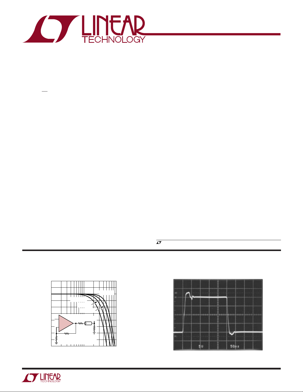
Cable Driver Frequency Response
2
0
VS = ±2.5V
–2
GAIN (dB)
–4
–6
–8
1
IN
+
LT1363
–
510Ω
VS = ±5V
75Ω
510Ω
FREQUENCY (MHz)
VS = ±10V
OUT
75Ω
10
U
AV = –1 Large-Signal Response
VS = ±15V
100
1363 TA02
1363 TA01
1
Page 2
LT1363
1
2
3
4
8
7
6
5
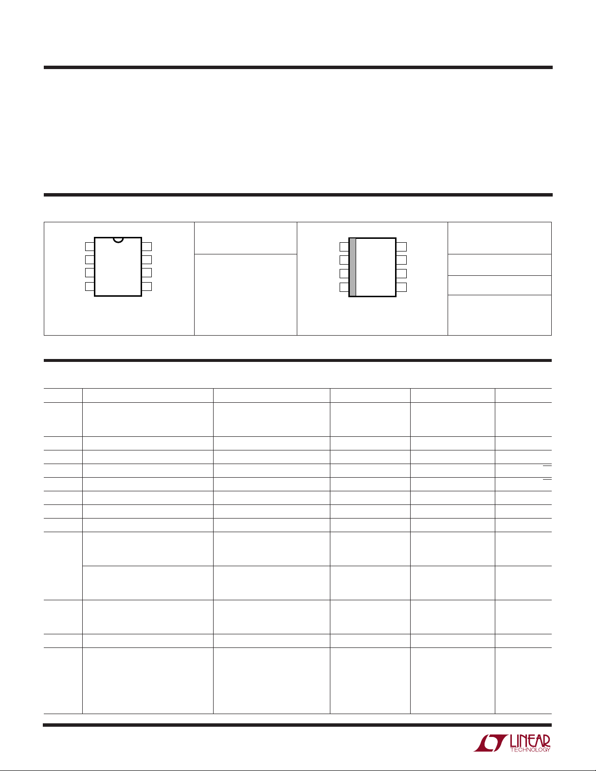
TOP VIEW
NULL
–IN
+IN
V
–
NULL
V
+
V
OUT
NC
N8 PACKAGE
8-LEAD PDIP
1
2
3
4
8
7
6
5
TOP VIEW
NULL
V
+
V
OUT
NC
NULL
–IN
+IN
V
–
S8 PACKAGE
8-LEAD PLASTIC SO
WW
W
ABSOLUTE MAXIMUM RATINGS
U
(Note 1)
Total Supply Voltage (V+ to V–) ............................... 36V
Differential Input Voltage
(Transient Only) (Note 2)................................... ±10V
Input Voltage ............................................................±V
Output Short-Circuit Duration (Note 3)............ Indefinite
U
W
PACKAGE/ORDER INFORMATION
ORDER PART
NUMBER
= 150°C, θJA = 130°C/ W
JMAX
Consult factory for Industrial and Military grade parts.
Operating Temperature Range (Note 8) ...–40°C to 85°C
Specified Temperature Range (Note 9)....–40°C to 85°C
Maximum Junction Temperature (See Below)
S
Plastic Package ................................................150°C
Storage Temperature Range ..................–65°C to 150°C
Lead Temperature (Soldering, 10 sec).................. 300°C
U
ORDER PART
NUMBER
LT1363CS8LT1363CN8
S8 PART MARKING
1363
T
= 150°C, θJA = 190°C/ WT
JMAX
T
ELECTRICAL CHARACTERISTICS
SYMBOL PARAMETER CONDITIONS V
V
OS
I
OS
I
B
e
n
i
n
R
IN
C
IN
CMRR Common Mode Rejection Ratio V
PSRR Power Supply Rejection Ratio VS = ±2.5V to ±15V 90 100 dB
A
VOL
2
Input Offset Voltage (Note 4) ±15V 0.5 1.5 mV
Input Offset Current ±2.5V to ±15V 120 350 nA
Input Bias Current ±2.5V to ±15V 0.6 2.0 µA
Input Noise Voltage f = 10kHz ±2.5V to ±15V 9 nV/√Hz
Input Noise Current f = 10kHz ±2.5V to ±15V 1 pA/√Hz
Input Resistance V
Input Resistance Differential ±15V 5 MΩ
Input Capacitance ±15V 3 pF
Input Voltage Range
Input Voltage Range
Large-Signal Voltage Gain V
+
–
= ±12V ±15V 12 50 MΩ
CM
= ±12V ±15V 84 90 dB
CM
V
= ±2.5V ±5V 76 81 dB
CM
V
= ±0.5V ±2.5V 66 71 dB
CM
= ±12V, RL = 1k ±15V 4.5 9.0 V/mV
OUT
V
= ±10V, RL = 500Ω±15V 3.0 6.5 V/mV
OUT
V
= ±7.5V, RL = 150Ω±15V 2.0 3.8 V/mV
OUT
V
= ±2.5V, RL = 500Ω±5V 3.0 6.4 V/mV
OUT
V
= ±2.5V, RL = 150Ω±5V 2.0 5.6 V/mV
OUT
V
= ±1V, RL = 500Ω±2.5V 2.5 5.2 V/mV
OUT
= 25°C, V
A
= 0V unless otherwise noted.
CM
SUPPLY
±5V 0.5 1.5 mV
±2.5V 0.7 1.8 mV
±15V 12.0 13.4 V
±5V 2.5 3.4 V
±2.5V 0.5 1.1 V
±15V –13.2 –12.0 V
±5V –3.2 –2.5 V
±2.5V –0.9 –0.5 V
MIN TYP MAX UNITS
Page 3
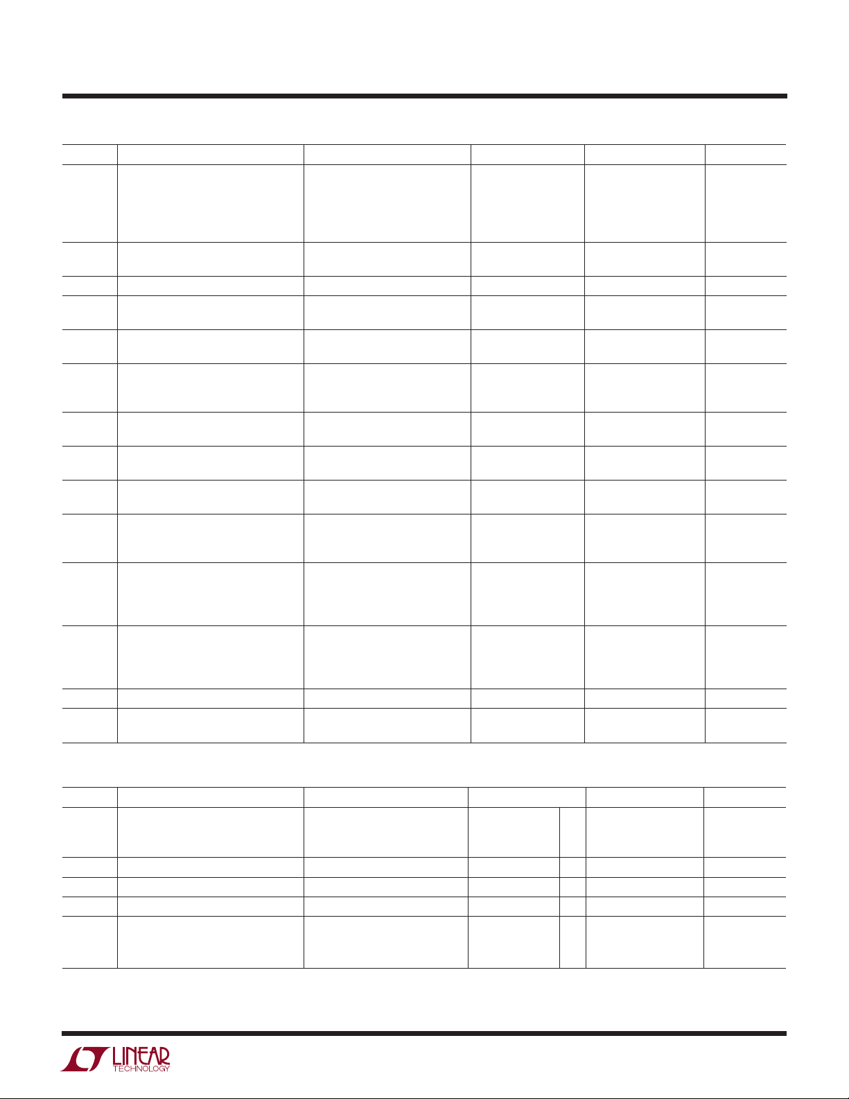
ELECTRICAL CHARACTERISTICS
T
= 25°C, V
A
= 0V unless otherwise noted.
CM
LT1363
SYMBOL PARAMETER CONDITIONS V
V
I
I
OUT
OUT
SC
Output Swing RL = 1k, V
R
= 500Ω, V
L
RL = 500Ω, V
R
= 150Ω, V
L
RL = 500Ω, V
Output Current V
Short-Circuit Current V
= ±7.5V ±15V 50 60 mA
OUT
V
= ±3.4V ±5V 23 29 mA
OUT
= 0V, V
OUT
= ±40mV ±15V 13.5 14.0 ±V
IN
= ±40mV ±15V 13.0 13.7 ±V
IN
= ±40mV ±5V 3.5 4.1 ±V
IN
= ±40mV ±5V 3.4 3.8 ±V
IN
= ±40mV ±2.5V 1.3 1.7 ±V
IN
= ±3V ±15V 70 105 mA
IN
SUPPLY
MIN TYP MAX UNITS
SR Slew Rate AV = –2, (Note 5) ±15V 750 1000 V/µs
±5V 300 450 V/µs
Full Power Bandwidth 10V Peak, (Note 6) ±15V 15.9 MHz
3V Peak, (Note 6) ±5V 23.9 MHz
GBW Gain Bandwidth f = 1MHz ±15V 70 MHz
±5V 50 MHz
±2.5V 40 MHz
tr, t
f
Rise Time, Fall Time AV = 1, 10%-90%, 0.1V ±15V 2.6 ns
±5V 3.6 ns
Overshoot AV = 1, 0.1V ±15V 36 %
±5V 23 %
Propagation Delay 50% VIN to 50% V
, 0.1V ±15V 4.6 ns
OUT
±5V 5.6 ns
t
s
Settling Time 10V Step, 0.1%, AV = –1 ±15V 50 ns
10V Step, 0.01%, A
= –1 ±15V 80 ns
V
5V Step, 0.1%, AV = –1 ±5V 55 ns
Differential Gain f = 3.58MHz, AV = 2, RL = 150Ω±15V 0.03 %
±5V 0.06 %
f = 3.58MHz, A
= 2, RL = 1k ±15V 0.01 %
V
±5V 0.01 %
Differential Phase f = 3.58MHz, AV = 2, RL = 150Ω±15V 0.10 Deg
±5V 0.04 Deg
f = 3.58MHz, A
= 2, RL = 1k ±15V 0.05 Deg
V
±5V 0.25 Deg
R
O
I
S
Output Resistance AV = 1, f = 1MHz ±15V 0.7 Ω
Supply Current ±15V 6.3 7.5 mA
±5V 6.0 7.2 mA
The ● denotes the specifications which apply over the temperature range 0°C ≤ TA ≤ 70°C, V
SYMBOL PARAMETER CONDITIONS V
V
OS
Input Offset Voltage (Note 4) ±15V ● 2.0 mV
Input VOS Drift (Note 7) ±2.5V to ±15V ● 10 13 µV/°C
I
OS
I
B
CMRR Common Mode Rejection Ratio V
Input Offset Current ±2.5V to ±15V ● 500 nA
Input Bias Current ±2.5V to ±15V ● 3 µA
= ±12V ±15V ● 82 dB
CM
= ±2.5V ±5V ● 74 dB
V
CM
V
= ±0.5V ±2.5V ● 64 dB
CM
SUPPLY
±5V
±2.5V
= 0V unless otherwise noted.
CM
MIN TYP MAX UNITS
● 2.0 mV
● 2.2 mV
3
Page 4
LT1363
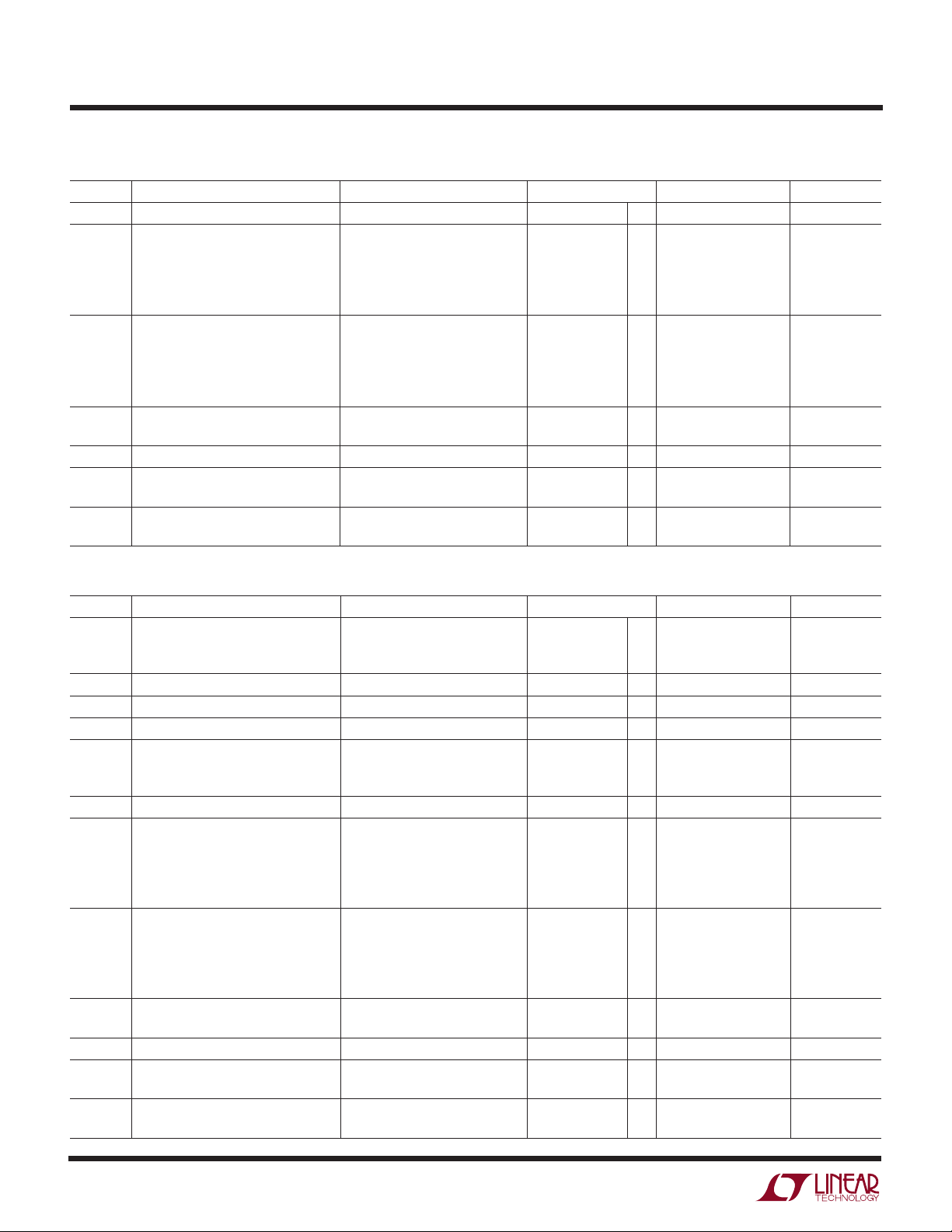
ELECTRICAL CHARACTERISTICS
0°C ≤ TA ≤ 70°C, V
SYMBOL PARAMETER CONDITIONS V
= 0V unless otherwise noted.
CM
The ● denotes the specifications which apply over the temperature range
SUPPLY
MIN TYP MAX UNITS
PSRR Power Supply Rejection Ratio VS = ±2.5V to ±15V ● 88 dB
A
V
I
I
VOL
OUT
OUT
SC
Large-Signal Voltage Gain V
= ±12V, RL = 1k ±15V ● 3.6 V/mV
OUT
V
= ±10V, RL = 500Ω±15V ● 2.4 V/mV
OUT
= ±2.5V, RL = 500Ω±5V ● 2.4 V/mV
V
OUT
= ±2.5V, RL = 150Ω±5V ● 1.5 V/mV
V
OUT
V
= ±1V, RL = 500Ω±2.5V ● 2.0 V/mV
OUT
Output Swing RL = 1k, V
= 500Ω, V
R
L
= 500Ω, V
R
L
R
= 150Ω, V
L
= 500Ω, V
R
L
Output Current V
Short-Circuit Current V
= ±12.8V ±15V ● 25 mA
OUT
= ±3.3V ±5V ● 22 mA
V
OUT
= 0V, V
OUT
= ±40mV ±15V ● 13.4 ±V
IN
= ±40mV ±15V ● 12.8 ±V
IN
= ±40mV ±5V ● 3.4 ±V
IN
= ±40mV ±5V ● 3.3 ±V
IN
= ±40mV ±2.5V ● 1.2 ±V
IN
= ±3V ±15V ● 55 mA
IN
SR Slew Rate AV = –2, (Note 5) ±15V ● 600 V/µs
±5V
I
S
Supply Current ±15V ● 8.7 mA
● 225 V/µs
±5V ● 8.4 mA
The ● denotes the specifications which apply over the temperature range –40°C ≤ TA ≤ 85°C, V
SYMBOL PARAMETER CONDITIONS V
V
OS
Input Offset Voltage (Note 4) ±15V ● 2.5 mV
SUPPLY
±5V
±2.5V
= 0V unless otherwise noted. (Note 9)
CM
MIN TYP MAX UNITS
● 2.5 mV
● 2.7 mV
Input VOS Drift (Note 7) ±2.5V to ±15V ● 10 13 µV/°C
I
OS
I
B
CMRR Common Mode Rejection Ratio V
Input Offset Current ±2.5V to ±15V ● 600 nA
Input Bias Current ±2.5V to ±15V ● 3.6 µA
= ±12V ±15V ● 82 dB
CM
V
= ±2.5V ±5V ● 74 dB
CM
= ±0.5V ±2.5V ● 64 dB
V
CM
PSRR Power Supply Rejection Ratio VS = ±2.5V to ±15V ● 87 dB
A
V
I
I
VOL
OUT
OUT
SC
Large-Signal Voltage Gain V
= ±12V, RL = 1k ±15V ● 2.5 V/mV
OUT
= ±10V, RL = 500Ω±15V ● 1.5 V/mV
V
OUT
V
= ±2.5V, RL = 500Ω±5V ● 1.5 V/mV
OUT
= ±2.5V, RL = 150Ω±5V ● 1.0 V/mV
V
OUT
= ±1V, RL = 500Ω±2.5V ● 1.3 V/mV
V
OUT
Output Swing RL = 1kΩ, V
R
= 500Ω, V
L
= 500Ω, V
R
L
= 150Ω, V
R
L
R
= 500Ω, V
L
Output Current V
Short-Circuit Current V
= ±12.7V ±15V ● 25 mA
OUT
= ±3.2V ±5V ● 21 mA
V
OUT
= 0V, V
OUT
= ±40mV ±15V ● 13.4 ±V
IN
= ±40mV ±15V ● 12.7 ±V
IN
= ±40mV ±5V ● 3.4 ±V
IN
= ±40mV ±5V ● 3.2 ±V
IN
= ±40mV ±2.5V ● 1.2 ±V
IN
= ±3V ±15V ● 50 mA
IN
SR Slew Rate AV = –2, (Note 5) ±15V ● 550 V/µs
±5V
I
S
Supply Current ±15V ● 9.0 mA
● 180 V/µs
±5V ● 8.7 mA
4
Page 5
ELECTRICAL CHARACTERISTICS
LT1363
Note 1: Absolute Maximum Ratings are those values beyond which the life
of a device may be impaired.
Note 2: Differential inputs of ±10V are appropriate for transient operation
only, such as during slewing. Large, sustained differential inputs will cause
excessive power dissipation and may damage the part. See Input
Considerations in the Applications Information section of this data sheet
for more details.
Note 3: A heat sink may be required to keep the junction temperature
below absolute maximum when the output is shorted indefinitely.
Note 4: Input offset voltage is pulse tested and is exclusive of warm-up drift.
Note 6: Full power bandwidth is calculated from the slew rate
measurement: FPBW = SR/2πV
Note 7: This parameter is not 100% tested.
Note 8: The LT1363C is guaranteed functional over the operating
temperature range of –40°C to 85°C.
Note 9: The LT1363C is guaranteed to meet specified performance from
0°C to 70°C. The LT1363C is designed, characterized and expected to
meet specified performance from –40°C to 85°C, but is not tested or QA
sampled at these temperatures. For guaranteed I-grade parts, consult the
factory.
Note 5: Slew rate is measured between ±10V on the output with ±6V input
for ±15V supplies and ±2V on the output with ±1.75V input for ±5V supplies.
W
U
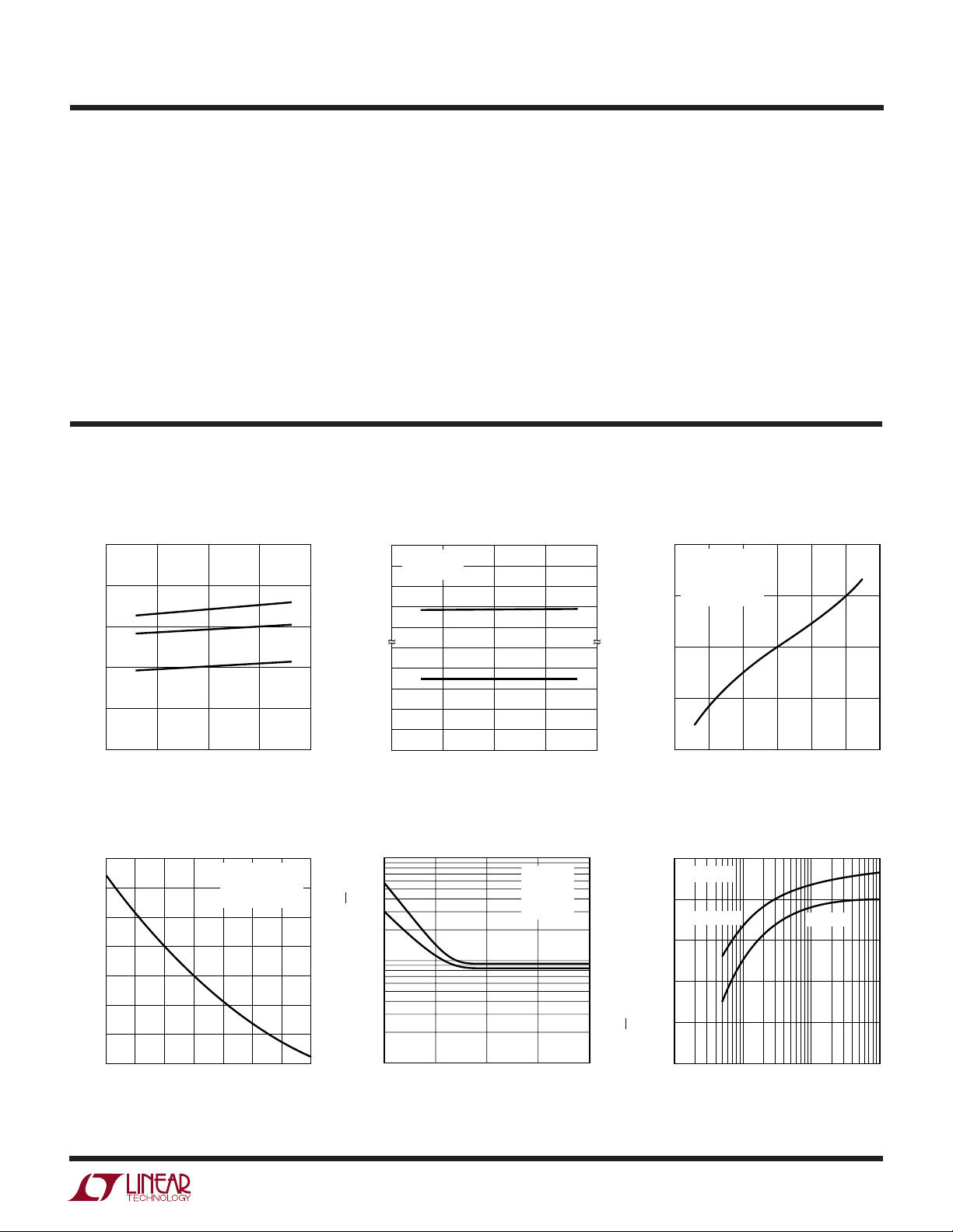
TYPICAL PERFORMANCE CHARACTERISTICS
Supply Current vs Supply Voltage
and Temperature
10
8
6
4
SUPPLY CURRENT (mA)
2
0
10501520
SUPPLY VOLTAGE (±V)
125°C
25°C
–55°C
1363 G01
Input Common Mode Range vs
Supply Voltage
+
V
TA = 25°C
–0.5
–1.0
–1.5
–2.0
2.0
1.5
COMMON MODE RANGE (V)
1.0
0.5
–
V
< 1mV
∆V
OS
SUPPLY VOLTAGE (±V)
10501520
1363 G02
.
P
Input Bias Current vs
Input Common Mode Voltage
1.0
VS = ±15V
= 25°C
T
A
+
–
I
+ I
B
I
B
0.8
0.6
0.4
INPUT BIAS CURRENT (µA)
0.2
–15 –10 0 10 155–5
B
=
————
2
INPUT COMMON MODE VOLTAGE (V)
1363 G03
Input Bias Current vs
Temperature
1.4
1.2
1.0
0.8
0.6
0.4
INPUT BIAS CURRENT (µA)
0.2
0
–50 –25 25 100 12550 750
TEMPERATURE (°C)
VS = ±15V
+
I
B
=
I
————
B
+ I
Open-Loop Gain vs
Input Noise Spectral Density
100
–
B
2
e
n
i
n
10
INPUT VOLTAGE NOISE (nV/√Hz)
1
10
1363 G04
FREQUENCY (Hz)
VS = ±15V
T
A
A
V
R
S
1k100 100k10k
= 25°C
= 101
= 100k
10
INPUT CURRENT NOISE (pA/√Hz)
1
0.1
1363 G05
Resistive Load
85
T
= 25°C
A
80
VS = ±15V
75
70
OPEN-LOOP GAIN (dB)
65
60
10
LOAD RESISTANCE (Ω)
VS = ±5V
100 10k
1k
1363 G06
5
Page 6
LT1363
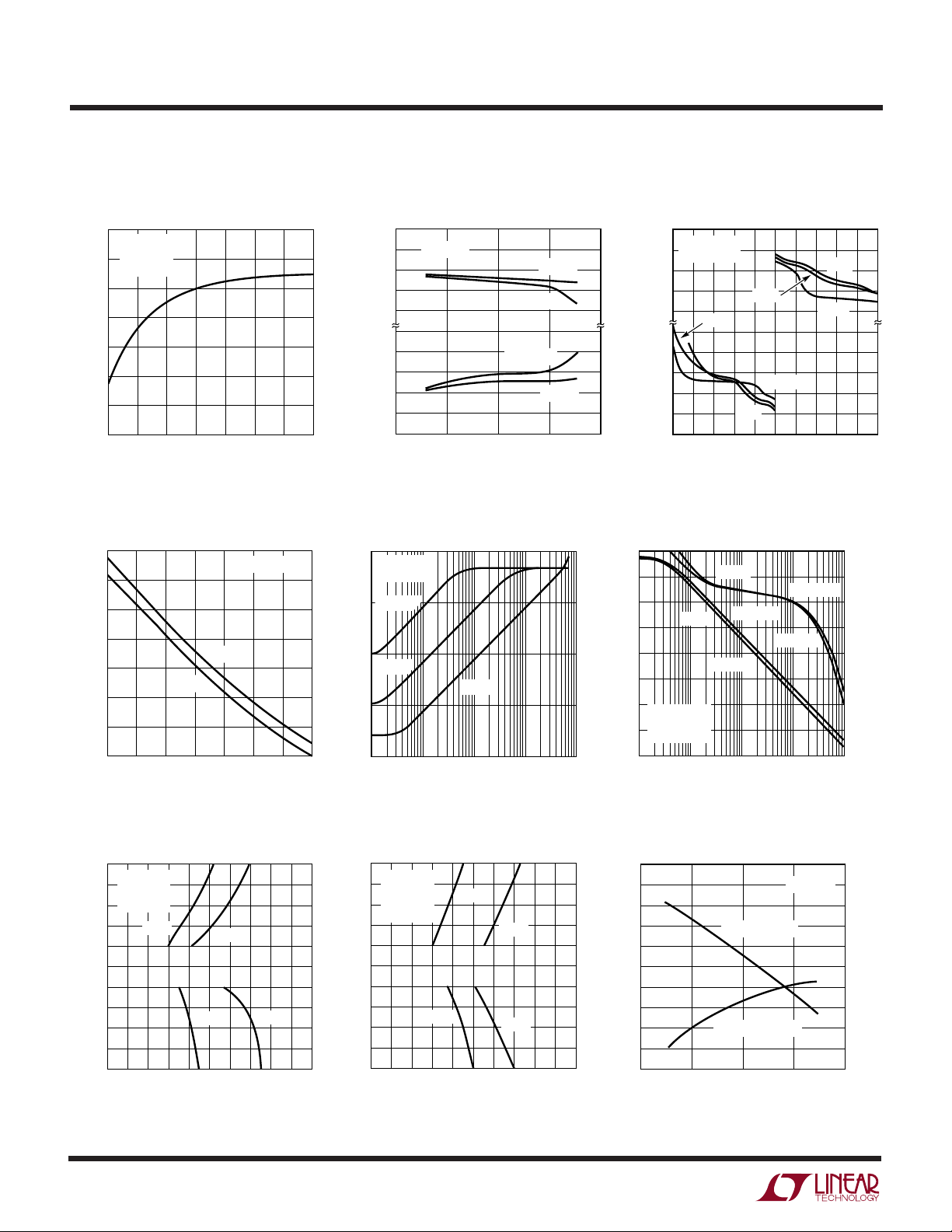
SUPPLY VOLTAGE (±V)
30
GAIN BANDWIDTH (MHz)
70
50
130
110
90
60
40
120
100
80
30
PHASE MARGIN (DEG)
38
34
50
48
44
40
36
32
46
42
10501520
1363 G15
TA = 25°C
PHASE MARGIN
GAIN BANDWIDTH
OUTPUT CURRENT (mA)
V
–
OUTPUT VOLTAGE SWING (V)
1.0
1.5
0.5
V
+
–0.5
–1.0
–1.5
2.0
–2.0
–50 –40 –10 30 40 5001020–20–30
1363 G09
VS = ±5V
V
IN
= 100mV
85°C
85°C
25°C
–40°C
–40°C
25°C
W
U
TYPICAL PERFORMANCE CHARACTERISTICS
81
RL = 1k
V
= ±12V
O
80
= ±15V
V
S
79
78
77
76
OPEN-LOOP GAIN (dB)
75
74
–50 –25 25 100 12550 750
TEMPERATURE (°C)
Output Short-Circuit Current vs
Temperature
140
130
120
110
100
90
80
OUTPUT SHORT-CIRCUIT CURRENT (mA)
70
–50 –25 25 100 12550 750
SOURCE
SINK
TEMPERATURE (°C)
VS = ±5V
1363 G07
1363 G10
Output Voltage Swing vs
Supply Voltage
+
V
–0.5
–1.0
–1.5
–2.0
2.0
1.5
OUTPUT VOLTAGE SWING (V)
1.0
0.5
V
TA = 25°C
–
Output Impedance vs
Frequency
100
VS = ±15V
= 25°C
T
A
AV = 100
10
1
AV = 10
0.1
OUTPUT IMPEDANCE (Ω)
0.01
10k
100k 100M
FREQUENCY (Hz)
RL = 1k
R
= 500Ω
L
R
= 500Ω
L
R
= 1k
L
10501520
SUPPLY VOLTAGE (±V)
1363 G08
Gain and Phase vs Frequency
70
60
50
40
30
GAIN (dB)
–10
20
10
0
10k
AV = 1
1M
10M
1363 G11
Output Voltage Swing vs
Load CurrentOpen-Loop Gain vs Temperature
PHASE
GAIN
= 25°C
T
A
= –1
A
V
R
= RG = 1k
F
100k 100M
VS = ±15V
VS = ±5V
1M
FREQUENCY (Hz)
VS = ±5V
10M
VS = ±15V
1363 G14
120
100
PHASE (DEG)
80
60
40
20
0
Settling Time vs Output Step
(Noninverting)
10
VS = ±15V
8
A
R
6
4
2
0
–2
OUTPUT STEP (V)
–4
–6
–8
–10
0 40 80 1006020
6
10
= 1
V
= 1k
L
10mV
SETTLING TIME (ns)
1mV
10mV
1mV
1363 G13
–2
OUTPUT STEP (V)
–4
–6
–8
–10
Settling Time vs Output Step
(Inverting)
VS = ±15V
8
= –1
A
R
6
C
4
2
0
0 40 80 1006020
V
= 1k
F
= 3pF
F
10mV
1mV
10mV
SETTLING TIME (ns)
1mV
Gain Bandwidth and Phase
Margin vs Supply Voltage
1363 G12
Page 7
W
U
TYPICAL PERFORMANCE CHARACTERISTICS
LT1363
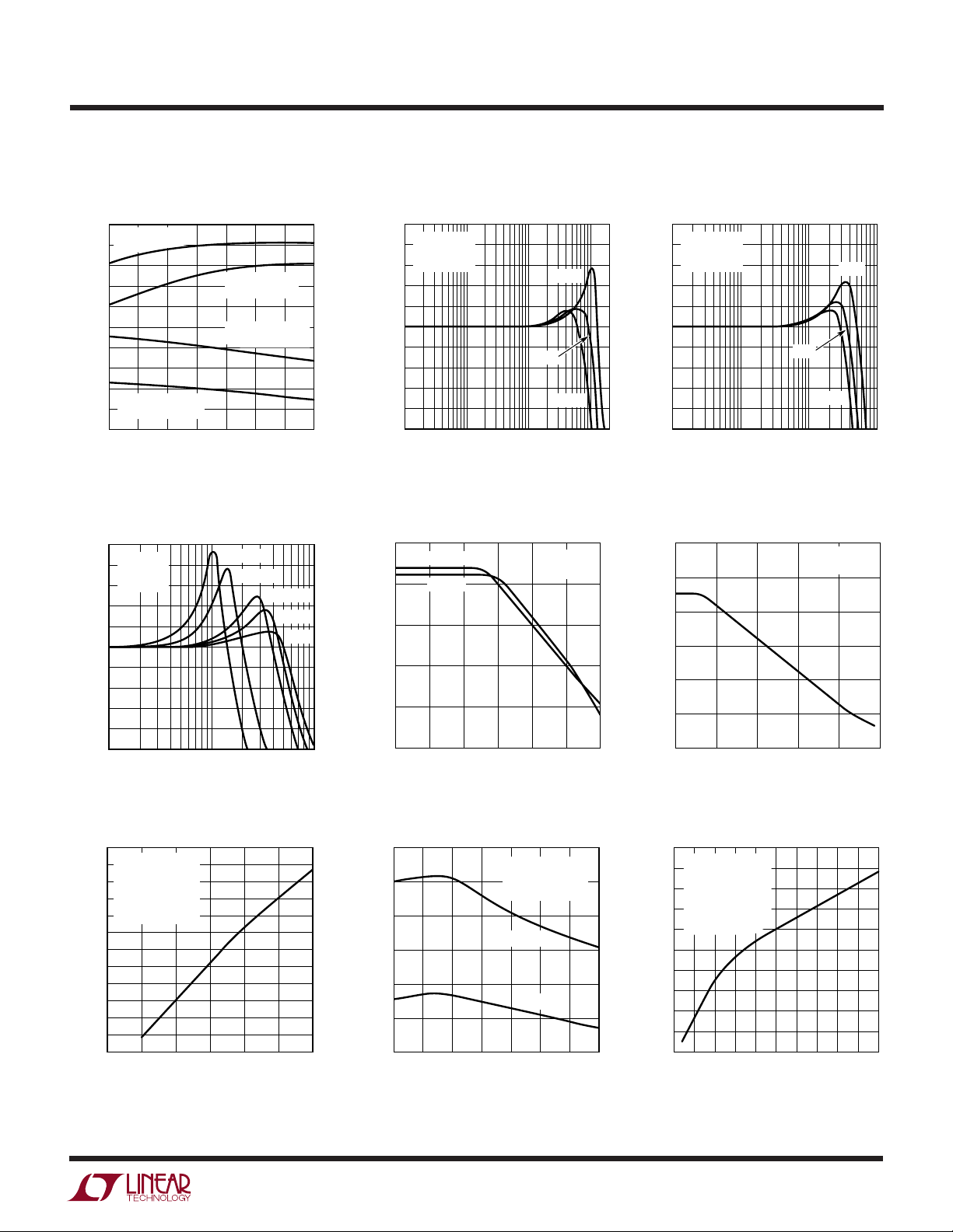
Gain Bandwidth and Phase
Margin vs Temperature
130
PHASE MARGIN
120
= ±5V
V
S
110
100
90
80
70
60
GAIN BANDWIDTH (MHz)
50
GAIN BANDWIDTH
40
= ±5V
V
S
30
–50 –25 25 100 12550 750
TEMPERATURE (°C)
Frequency Response vs
Capacitive Load
15
VS = ±15V
12
= 25°C
T
A
A
= –1
9
V
6
3
0
–3
–6
VOLTAGE MAGNITUDE (dB)
–9
–12
–15
1M
10M
FREQUENCY (Hz)
PHASE MARGIN
V
= ±15V
S
GAIN BANDWIDTH
= ±15V
V
S
C = 1000pF
C = 500pF
C = 100pF
C = 50pF
1363 G16
C = 0
1363 G19
50
45
40
PHASE MARGIN (DEG)
35
30
25
20
15
10
5
0
100M
Frequency Response vs
Supply Voltage (AV = 1)
10
T
= 25°C
A
8
= 1
A
V
= 1k
R
6
L
4
2
0
GAIN (dB)
–2
–4
–6
–8
–10
100k
1M 100M
FREQUENCY (Hz)
10M
Power Supply Rejection Ratio
vs Frequency
100
80
60
40
20
POWER SUPPLY REJECTION RATIO (dB)
0
+PSRR
–PSRR
100k 1M1k 10k100 10M 100M
FREQUENCY (Hz)
±15V
±5V
±2.5V
VS = ±15V
= 25°C
T
A
1363 G17
1363 G20
Frequency Response vs
Supply Voltage (AV = –1)
5
T
= 25°C
A
4
= –1
A
V
= RG = 1k
R
3
F
2
1
0
GAIN (dB)
–1
–2
–3
–4
–5
100k
1M 100M
FREQUENCY (Hz)
±5V
10M
Common Mode Rejection Ratio
vs Frequency
120
100
80
60
40
20
COMMON-MODE REJECTION RATIO (dB)
0
1k 100M10M1M100k10k
FREQUENCY (Hz)
±2.5V
VS = ±15V
T
= 25°C
A
±15V
1363 G18
1363 G21
Slew Rate vs Supply Voltage Slew Rate vs Input LevelSlew Rate vs Temperature
2400
2200
2000
1800
1600
1400
1200
1000
800
SLEW RATE (V/µs)
600
400
200
0
015105
TA = 25°C
A
= –1
V
= RG = 1k
R
F
SR+ + SR
SR =
—————
2
SUPPLY VOLTAGE (±V)
–
1363 G22
1400
1200
1000
800
600
SLEW RATE (V/µs)
400
200
–50 –25 25 100 12550 750
TEMPERATURE (°C)
A
= –2
V
SR = —————
V
= ±15V
S
V
SR+ + SR
2
= ±5V
S
–
1363 G23
2000
1800
1600
1400
1200
1000
SLEW RATE (V/µS)
800
600
400
200
0
TA = 25°C
= ±15V
V
S
A
= –1
V
= RG = 1k
R
F
SR+ + SR
SR =
—————
0 8 16 2012421018146
–
2
INPUT LEVEL (V
P-P
)
1363 G24
7
Page 8
LT1363
W
U
TYPICAL PERFORMANCE CHARACTERISTICS
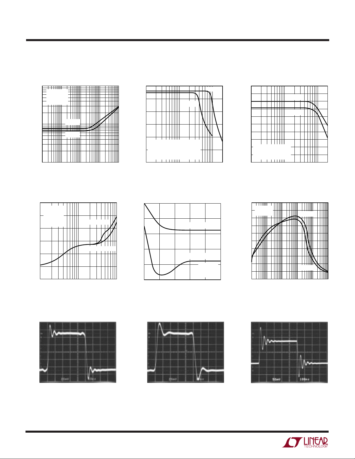
Total Harmonic Distortion
vs Frequency
0.01
TA = 25°C
= 3V
V
O
RMS
RL = 500Ω
0.001
TOTAL HARMONIC DISTORTION (%)
0.0001
10
AV = –1
AV = 1
100 100k
1k
FREQUENCY (Hz)
2nd and 3rd Harmonic Distortion
vs Frequency
–40
VS = ±15V
= 2V
V
O
–50
–60
–70
–80
HARMONIC DISTORTION (dB)
–90
–100
100k 200k 400k
P-P
RL = 500Ω
= 2
A
V
3RD HARMONIC
2ND HARMONIC
1M 2M 4M
FREQUENCY (Hz)
10k
1363 G25
1363 G28
10M
Undistorted Output Swing vs
Frequency (±15V)
30
25
)
P-P
20
15
10
VS = ±15V
OUTPUT VOLTAGE (V
= 1k
R
L
5
= 1, 1% MAX DISTORTION
A
V
= –1, 2% MAX DISTORTION
A
V
0
100k 1M
FREQUENCY (Hz)
Differential Gain and Phase
vs Supply Voltage
DIFFERENTIAL GAIN
0.3
0.2
DIFFERENTIAL PHASE
0.1
DIFFERENTIAL PHASE (DEG)
0.0
SUPPLY VOLTAGE (V)
AV = –1
AV = 1
10M
1363 G26
AV = 2
= 150Ω
R
L
= 25°C
T
A
±10±5 ±15
1363 G29
Undistorted Output Swing vs
Frequency (±5V)
10
8
)
P-P
6
4
OUTPUT VOLTAGE (V
2
0
100k 1M
DIFFERENTIAL GAIN (%)
0.2
0.1
0
Capacitive Load Handling
100
50
OVERSHOOT (%)
0
10p
AV = –1
AV = 1
VS = ±5V
= 1k
R
L
2% MAX DISTORTION
FREQUENCY (Hz)
TA = 25°C
= ±15V
V
S
1000p 0.01µ
100p 0.1µ
CAPACITIVE LOAD (F)
10M
1363 G27
AV = –1
AV = 1
1µ
1363 G30
Small-Signal Transient
(AV = 1)
8
Small-Signal Transient
(AV = –1)
1363 TA31 1363 TA32
Small-Signal Transient
(AV = –1, CL = 200pF)
1363 TA33
Page 9
W
U
TYPICAL PERFORMANCE CHARACTERISTICS
LT1363
Large-Signal Transient
(AV = 1)
1363 TA34 1363 TA35
U
Large-Signal Transient
(AV = –1)
WUU
APPLICATIONS INFORMATION
The LT1363 may be inserted directly into AD817, AD847,
EL2020, EL2044, and LM6361 applications improving
both DC and AC performance, provided that the nulling
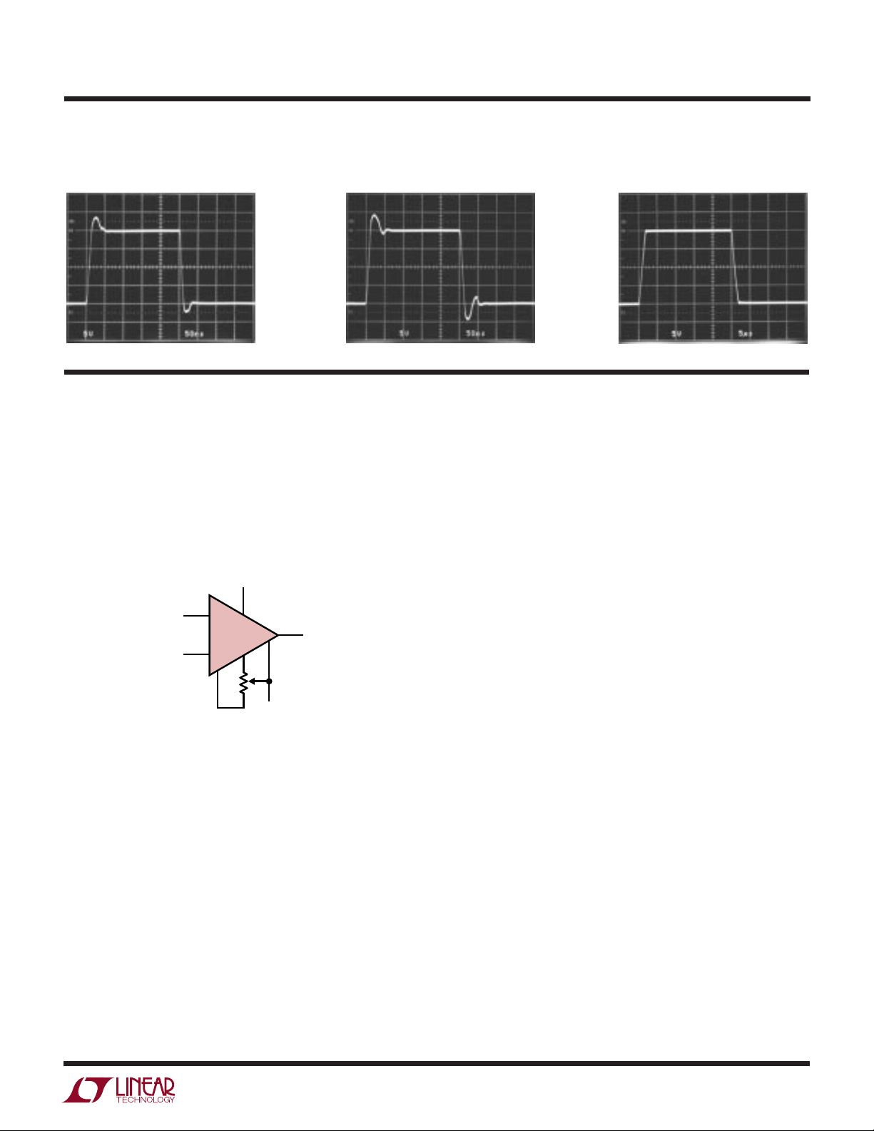
circuitry is removed. The suggested nulling circuit for the
LT1363 is shown below.
Offset Nulling
+
V
3
2
Layout and Passive Components
The LT1363 amplifier is easy to apply and tolerant of less
than ideal layouts. For maximum performance (for example fast settling time) use a ground plane, short lead
lengths, and RF-quality bypass capacitors (0.01µF to
0.1µF). For high drive current applications use low ESR
bypass capacitors (1µF to 10µF tantalum). Sockets
should be avoided when maximum frequency performance is required, although low profile sockets can
provide reasonable performance up to 50MHz. For
more details see Design Note 50.
+
–
1
LT1363
10k
7
6
4
8
–
V
1363 AI01
Large-Signal Transient
(AV = 1, CL = 10,000pF)
1363 TA36
The parallel combination of the feedback resistor and gain
setting resistor on the inverting input can combine with
the input capacitance to form a pole which can cause
peaking or oscillations. For feedback resistors greater
than 5kΩ, a parallel capacitor of value
CF > RG x CIN/R
F
should be used to cancel the input pole and optimize
dynamic performance. For unity-gain applications where
a large feedback resistor is used, CF should be greater
than or equal to CIN.
Capacitive Loading
The LT1363 is stable with any capacitive load. This is
accomplished by sensing the load induced output pole and
adding compensation at the amplifier gain node. As the
capacitive load increases, both the bandwidth and phase
margin decrease so there will be peaking in the frequency
domain and in the transient response as shown in the
typical performance curves.The photo of the small-signal
response with 200pF load shows 62% peaking. The largesignal response with a 10,000pF load shows the output
slew rate being limited to 10V/µs by the short-circuit
current. Coaxial cable can be driven directly, but for best
pulse fidelity a resistor of value equal to the characteristic
impedance of the cable (i.e., 75Ω) should be placed in
series with the output. The other end of the cable should
be terminated with the same value resistor to ground. The
response of a cable driver in a gain of 2 driving a 75Ω cable
is shown on the front page of the data sheet.
9
Page 10

LT1363
U
WUU
APPLICATIONS INFORMATION
Input Considerations
Each of the LT1363 inputs is the base of an NPN and a PNP
transistor whose base currents are of opposite polarity
and provide first-order bias current cancellation. Because
of variation in the matching of NPN and PNP beta, the
polarity of the input bias current can be positive or negative. The offset current does not depend on NPN/PNP beta
matching and is well controlled. The use of balanced
source resistance at each input is recommended for
applications where DC accuracy must be maximized.
The inputs can withstand transient differential input voltages up to 10V without damage and need no clamping or
source resistance for protection. Differential inputs, however, generate large supply currents (tens of mA) as
required for high slew rates. If the device is used with
sustained differential inputs, the average supply current
will increase, excessive power dissipation will result and
the part may be damaged. The part should not be used as
a comparator, peak detector or other open-loop application with large, sustained differential inputs. Under
normal, closed-loop operation, an increase of power dissipation is only noticeable in applications with large slewing
outputs and is proportional to the magnitude of the
differential input voltage and the percent of the time that
the inputs are apart. Measure the average supply current
for the application in order to calculate the power dissipation.
Single Supply Operation
The LT1363 is specified at ±15V, ±5V, and ±2.5V supplies,
but it is also well suited to single supply operation down
to a single 5V supply. The symmetrical input Ccmmon
mode range and output swing make the device well suited
for applications with a single supply if the the input and
output swing ranges are centered (i.e., a DC bias of 2.5V
on the input and the output). For 5V video applications
with an assymetrical swing, an offset of 2V on the input
works best.
Power Dissipation
The LT1363 combines high speed and large output drive
in a small package. Because of the wide supply voltage
range, it is possible to exceed the maximum junction
temperature under certain conditions. Maximum junction
temperature (TJ) is calculated from the ambient temperature (TA) and power dissipation (PD) as follows:
LT1363CN8: TJ = TA + (PD x 130°C/W)
LT1363CS8: TJ = TA + (PD x 190°C/W)
Worst case power dissipation occurs at the maximum
supply current and when the output voltage is at 1/2 of
either supply voltage (or the maximum swing if less than
1/2 supply voltage). Therefore P
P
Example: LT1363CS8 at 70°C, VS = ±15V, RL = 390Ω
P
T
Circuit Operation
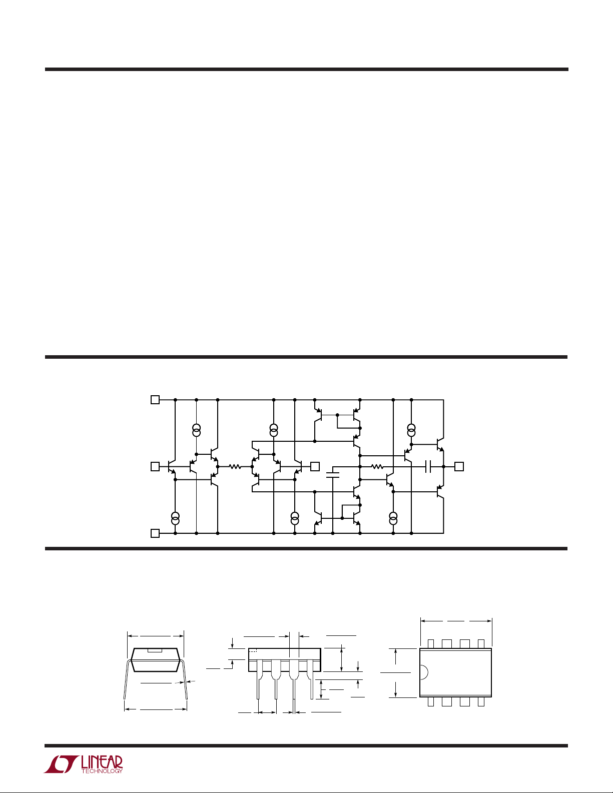
The LT1363 circuit topology is a true voltage feedback
amplifier that has the slewing behavior of a current feedback amplifier. The operation of the circuit can be understood by referring to the simplified schematic. The inputs
are buffered by complementary NPN and PNP emitter
followers which drive a 500Ω resistor. The input voltage
appears across the resistor generating currents which are
mirrored into the high impedance node. Complementary
followers form an output stage which buffers the gain
node from the load. The bandwidth is set by the input
resistor and the capacitance on the high impedance node.
The slew rate is determined by the current available to
charge the gain node capacitance. This current is the
differential input voltage divided by R1, so the slew rate is
proportional to the input. Highest slew rates are therefore
seen in the lowest gain configurations. For example, a 10V
output step in a gain of 10 has only a 1V input step,
whereas the same output step in unity gain has a 10 times
greater input step. The curve of Slew Rate vs Input Level
illustrates this relationship. The LT1363 is tested for slew
rate in a gain of –2 so higher slew rates can be expected
in gains of 1 and –1, and lower slew rates in higher gain
configurations.
= (V+ – V–)(I
DMAX
= (30V)(8.7mA) + (7.5V)2/390Ω = 405mW
DMAX
= 70°C + (405mW)(190°C/W) = 147°C
JMAX
) + (V+/2)2/R
SMAX
DMAX
is:
L
10
Page 11
LT1363
U
WUU
APPLICATIONS INFORMATION
The RC network across the output stage is bootstrapped
when the amplifier is driving a light or moderate load and
has no effect under normal operation. When driving a
capacitive load (or a low value resistive load) the network
is incompletely bootstrapped and adds to the compensation at the high impedance node. The added capacitance
slows down the amplifier which improves the phase
margin by moving the unity-gain frequency away from the
pole formed by the output impedance and the capacitive
load. The zero created by the RC combination adds phase
to ensure that even for very large load capacitances, the
total phase lag can never exceed 180 degrees (zero phase
margin) and the amplifier remains stable.
Comparison to Current Feedback Amplifiers
The LT1363 enjoys the high slew rates of Current Feedback Amplifiers (CFAs) while maintaining the characteris-
E
W
A
TI
C
W
SPL
I
IIFED S
CH
+
V
tics of a true voltage feedback amplifier. The primary
differences are that the LT1363 has two high impedance
inputs and its closed loop bandwidth decreases as the gain
increases. CFAs have a low impedance inverting input and
maintain relatively constant bandwidth with increasing
gain. The LT1363 can be used in all traditional op amp
configurations including integrators and applications such
as photodiode amplifiers and I-to-V converters where
there may be significant capacitance on the inverting
input. The frequency compensation is internal and not
dependent on the value of the feedback resistor. For CFAs,
the feedback resistance is fixed for a given bandwidth and
capacitance on the inverting input can cause peaking or
oscillations. The slew rate of the LT1363 in noninverting
gain configurations is also superior in most cases.
–IN
–
V
PACKAGE DESCRIPTION
0.300 – 0.325
(7.620 – 8.255)
0.065
(1.651)
0.009 – 0.015
(0.229 – 0.381)
+0.035
0.325
–0.015
+0.889
8.255
()
–0.381
*THESE DIMENSIONS DO NOT INCLUDE MOLD FLASH OR PROTRUSIONS.
MOLD FLASH OR PROTRUSIONS SHALL NOT EXCEED 0.010 INCH (0.254mm)
TYP
R1
500Ω
+IN
C
R
C
C
C
U
Dimension in inches (millimeters) unless otherwise noted.
N8 Package
8-Lead PDIP (Narrow 0.300)
(LTC DWG # 05-08-1510)
0.045 – 0.065
(1.143 – 1.651)
0.100
(2.54)
BSC
0.130 ± 0.005
(3.302 ± 0.127)
0.125
(3.175)
MIN
0.018 ± 0.003
(0.457 ± 0.076)
0.020
(0.508)
MIN
876
0.255 ± 0.015*
(6.477 ± 0.381)
1234
1363 SS01
0.400*
(10.160)
MAX
OUT
5
N8 1098
Information furnished by Linear Technology Corporation is believed to be accurate and reliable.
However, no responsibility is assumed for its use. Linear Technology Corporation makes no representation that the interconnection of its circuits as described herein will not infringe on existing patent rights.
11
Page 12
LT1363
TYPICAL APPLICATIONS
U
Two Op Amp Instrumentation Amplifier
R5
220Ω
R1
10k
–
V
IN
–
LT1363
+
R2
1k
R3
1k
–
LT1363
+
+
RRR
+
R
4
R
4
12213
GAIN
TRIM R5 FOR GAIN
TRIM R1 FOR COMMON-MODE REJECTION
BW = 700kHz
=
1
+
R
3
RR
23
+
()
=
+
102
R
5
PACKAGE DESCRIPTION
0.010 – 0.020
(0.254 – 0.508)
0.008 – 0.010
(0.203 – 0.254)
*
DIMENSION DOES NOT INCLUDE MOLD FLASH. MOLD FLASH
SHALL NOT EXCEED 0.006" (0.152mm) PER SIDE
**
DIMENSION DOES NOT INCLUDE INTERLEAD FLASH. INTERLEAD
FLASH SHALL NOT EXCEED 0.010" (0.254mm) PER SIDE
× 45°
0.016 – 0.050
(0.406 – 1.270)
0.053 – 0.069
(1.346 – 1.752)
0°– 8° TYP
0.014 – 0.019
(0.355 – 0.483)
2MHz, 4th Order Butterworth Filter
10k
R4
V
IN
V
OUT
1363 TA03
1.33k464Ω
220pF
464Ω
47pF
–
LT1363
+
U
Dimension in inches (millimeters) unless otherwise noted.
S8 Package
8-Lead Plastic Small Outline (Narrow 0.150)
(LTC DWG # 05-08-1610)
8
0.004 – 0.010
(0.101 – 0.254)
0.228 – 0.244
(5.791 – 6.197)
1
TYP
0.050
(1.270)
BSC
549Ω
1.13k
470pF
0.189 – 0.197*
(4.801 – 5.004)
7
2
549Ω
22pF
–
LT1363
V
OUT
+
1363 TA04
5
6
0.150 – 0.157**
(3.810 – 3.988)
3
4
SO8 1298
RELATED PARTS
PART NUMBER DESCRIPTION COMMENTS
LT1364/LT1365 Dual and Quad 70MHz, 1000V/µs Op Amps Dual and Quad Versions of LT1363
LT1360 50MHz, 800V/µs Op Amp Lower Power Version of LT1363, VOS = 1mV, IS = 4mA
LT1357 25MHz, 600V/µs Op Amp Lower Power Version of LT1363, VOS = 0.6mV, IS = 2mA
LT1812 100MHz, 750V/µs Op Amp Low Voltage, Low Power LT1363, VOS = 1.5mV, IS = 3mA
1363fa LT/TP 0400 2K REV A • PRINTED IN USA
LINEAR TECHNOLOGY CORPORATION 1994
12
Linear Technology Corporation
1630 McCarthy Blvd., Milpitas, CA 95035-7417
(408) 432-1900 ● FAX: (408) 434-0507
●
www.linear-tech.com
 Loading...