

Page 1
LT1312
Single PCMCIA
OBSOLETE:
FOR INFORMATION PURPOSES ONLY
Contact Linear Technology for Potential Replacement
FEATURES
■
Digital Selection of 0V, VCC, 12V or Hi-Z
■
120mA Output Current Capability
■
Internal Current Limiting and Thermal Shutdown
■
Automatic Switching from 3.3V to 5V
■
Powered from Unregulated 13V to 20V Supply
■
Logic Compatible with Standard PCMCIA Controllers
■
1µF Output Capacitor
■
30µA Quiescent Current in Hi-Z or 0V Mode
■
VPP Valid Status Feedback Signal
■
No VPP Overshoot
■
8-Pin SO Packaging
U
APPLICATIONS
■
Notebook Computers
■
Palmtop Computers
■
Pen-Based Computers
■
Handi-Terminals
■
Bar-Code Readers
■
Flash Memory Programming
VPP Driver/Regulator
U
DESCRIPTION
The LT®1312 is a member of Linear Technology
Corporation’s family of PCMCIA drivers/regulators. The
LT1312 provides 0V, 3.3V, 5V, 12V and Hi-Z regulated
power to the VPP pin of a PCMCIA card slot from a single
unregulated 13V to 20V supply. When used in conjunction
with a PC card interface controller, the LT1312 forms a
complete minimum component-count interface for palmtop, pen-based and notebook computers. The VPP output
voltage is selected by two logic compatible digital inputs
which interface directly with industry standard PC card
interface controllers.
Automatic 3.3V to 5V switching is provided by an internal
comparator which continuously monitors the PC card V
supply and automatically adjusts the regulated VPP output to match VCC when the VPP = VCC mode is selected.
An open-collector VPP VALID output is driven low when
VPP is in regulation at 12V.
The LT1312 is available in an 8-pin SO package.
, LTC and LT are registered trademarks of Linear Technology Corporation.
CC
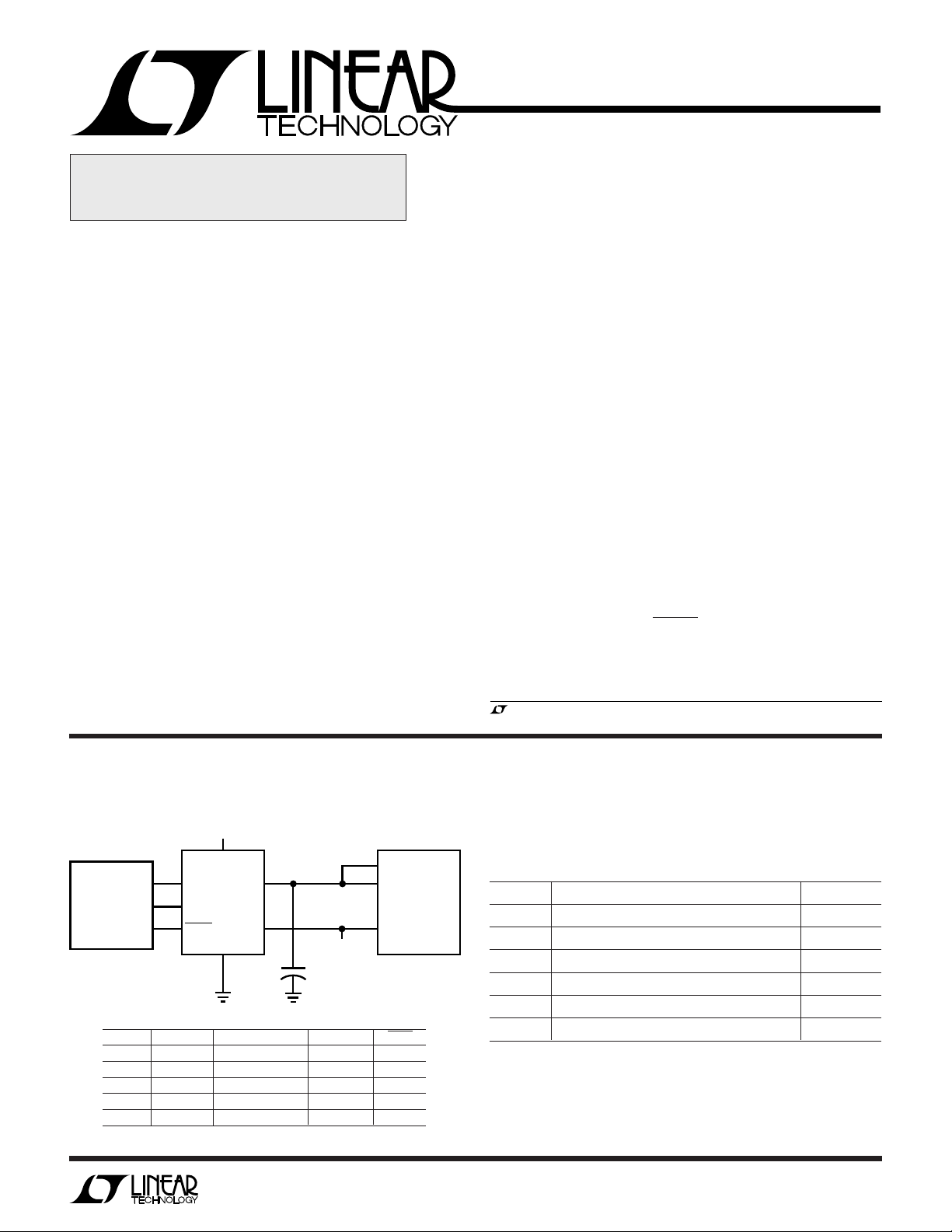
TYPICAL APPLICATION
Typical PCMCIA Single Slot VPP Driver
13V TO 20V
V
S
VPP
PCMCIA
CARD SLOT
CONTROLLER
LT1312 TRUTH TABLE
EN0 EN1 SENSE VPP
00 X 0V 1
1 0 X 12V 0
0 1 3.0V TO 3.6V 3.3V 1
0 1 4.5V TO 5.5V 5V 1
1 1 X Hi-Z 1
X = DON’T CARE
EN0
VALID SENSE
LT1312EN1
GND
OUT
+
C
1µF
TANTALUM
U
3.3V OR 5V
OUT
OUT
VPP1
VPP2
PCMCIA
CARD SLOT
V
CC
VALID
LT1312 TA1
Linear Technology PCMCIA Product Family
DEVICE DESCRIPTION PACKAGE
LT1312 SINGLE PCMCIA VPP DRIVER/REGULATOR 8-PIN SO
LT1313 DUAL PCMCIA VPP DRIVER/REGULATOR 16-PIN SO*
LTC®1314 SINGLE PCMCIA SWITCH MATRIX 14-PIN SO
LTC1315 DUAL PCMCIA SWITCH MATRIX 24-PIN SSOP
LTC1470 PROTECTED VCC 5V/3.3V SWITCH MATRIX 8-PIN SO
LTC1472 PROTECTED VCC AND VPP SWITCH MATRIX 16-PIN SO*
*NARROW BODY
1
Page 2
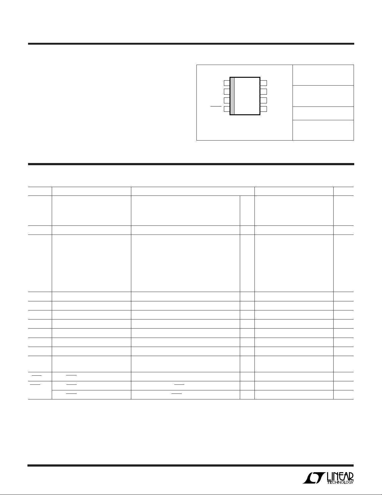
LT1312
1
2
3
4
8
7
6
5
TOP VIEW
S8 PACKAGE
8-LEAD PLASTIC SO
GND
ENO
EN1
VALID
VPP
OUT
N.C.
V
S
SENSE
WW
W
ABSOLUTE MAXIMUM RATINGS
Supply Voltage ........................................................ 22V
Digital Input Voltage ........................ 7V to (GND – 0.3V)
U
U
W
PACKAGE/ORDER INFORMATION
ORDER PART
NUMBER
U
Sense Input Voltage......................... 7V to (GND – 0.3V)
Valid Output Voltage ...................... 15V to (GND – 0.3V)
LT1312CS8
Output Short-Circuit Duration.......................... Indefinite
Operating Temperature ................................ 0°C to 70°C
S8 PART MARKING
Junction Temperature................................ 0°C to 125°C
Storage Temperature Range ..................–65°C to 150°C
T
= 125°C, θJA = 150°C/W
JMAX
1312
Lead Temperature (Soldering, 10 sec).................. 300°C
Consult factory for Industrial and Military grade parts.
ELECTRICAL CHARACTERISTICS
SYMBOL PARAMETER CONDITIONS MIN TYP MAX UNITS
VPP
OUT
I
LKG
I
S
I
LIM
V
ENH
V
ENL
I
ENH
I
ENL
V
SEN5
V
SEN3
I
SEN
V
VALID TH
I
VALID
The ● denotes the specifications which apply over the full operating
temperature range.
Output Voltage Program to 12V, I
Program to 5V, I
Program to 3.3V, I
Program to 0V, I
Output Leakage Program to Hi-Z, 0V ≤ VPP
Supply Current Program to 0V ● 30 50 µA
Program to Hi-Z
Program to 12V, No Load
Program to 5V, No Load
Program to 3.3V, No Load
Program to 12V, I
Program to 5V, I
Program to 3.3V, I
Current Limit Program to 3.3V, 5V or 12V 330 500 mA
Enable Input High Voltage ● 2.4 V
Enable Input Low Voltage ● 0.4 V
Enable Input High Current 2.4V ≤ VIN ≤ 5.5V 20 50 µA
Enable Input Low Current 0V ≤ VIN ≤ 0.4V 0.01 1 µA
VCC Sense Threshold VPP
VCC Sense Threshold VPP
VCC Sense Input Current V
VPP
VPP
VPP
Threshold Voltage Program to 12V ● 10.5 11 11.5 V
VALID
Output Drive Current Program to 12V, V
VALID
Output Leakage Current Program to 0V, V
VALID
OUT
OUT
= 5V 38 60 µA
SENSE
V
= 3.3V 18 30 µA
SENSE
VS = 13V to 20V, TA = 25°C, unless otherwise noted.
≤ 120mA (Note 1) ● 11.52 12.00 12.48 V
OUT
≤ 30mA (Note 1) ● 4.75 5.00 5.25 V
OUT
≤ 30mA (Note 1) ● 3.135 3.30 3.465 V
OUT
= –300µA 0.42 0.60 V
OUT
≤ 12V ● –10 10 µA
OUT
● 30 50 µA
● 230 360 µA
● 75 120 µA
● 55 90 µA
= 120mA ● 126 132 mA
OUT
= 30mA ● 31 33 mA
OUT
= 30mA ● 31 33 mA
OUT
= 3.3V to 5V ● 3.60 4.05 4.50 V
= 5V to 3.3V ● 3.60 4.00 4.50 V
= 0.4V 1 3.3 mA
VALID
= 12V 0.1 10 µA
VALID
Note 1: For junction temperatures greater than 110°C, a minimum load
of 1mA is recommended.
2
Page 3
W
U
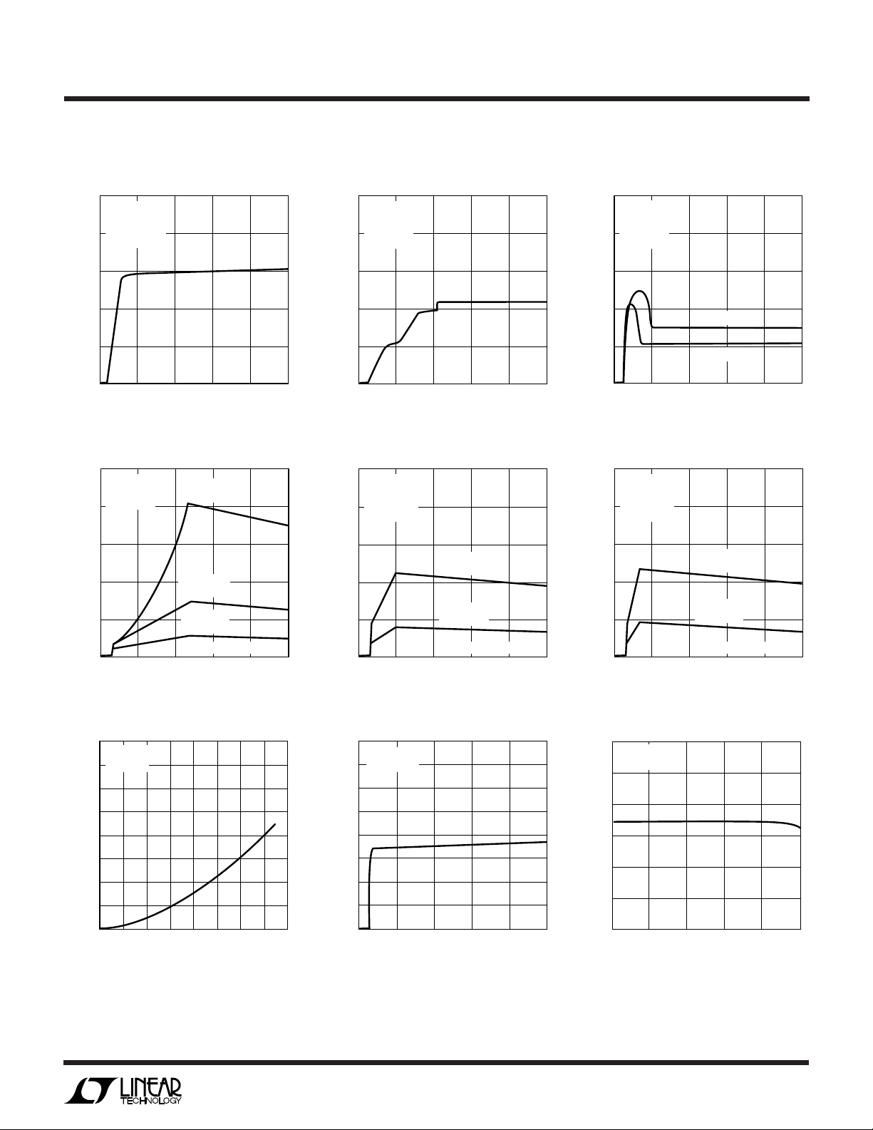
TYPICAL PERFORMANCE CHARACTERISTICS
LT1312
Quiescent Current (12V Mode)Quiescent Current (0V or Hi-Z Mode)
50
TJ = 25°C
EN0 = EN1= 0V
OR
40
EN0 = EN1= 5V
30
20
QUIESCENT CURRENT (µA)
10
0
5
0
10
SUPPLY VOLTAGE (V)
15
20
25
LT1312 G1
500
TJ = 25°C
EN0 = 5V
EN1 = 0V
400
=
∞
R
L
300
200
QUIESCENT CURRENT (µA)
100
0
5
0
SUPPLY VOLTAGE (V)
15
10
Ground Pin Current (12V Mode) Ground Pin Current (5V Mode)
10
TJ = 25°C
EN0 = 5V
EN1 = 0V
8
6
4
GROUND CURRENT (mA)
2
0
5
0
SUPPLY VOLTAGE (V)
R
L
I
= 60mA*
L
R
L
= 30mA*
I
L
*FOR VPP
10
= 100
R
L
= 120mA*
I
L
= 200
= 400
15
Ω
Ω
OUT
Ω
= 12V
20
25
LT1312 G4
2.5
TJ = 25°C
EN0 = 0V
EN1 = 5V
2.0
1.5
1.0
GROUND CURRENT (mA)
0.5
0
= 5V
V
SENSE
5
0
SUPPLY VOLTAGE (V)
R
L
I
L
R
= 500Ω
L
= 10mA*
I
L
*FOR VPP
10
= 167Ω
= 30mA*
15
OUT
= 5V
Quiescent Current (3.3V/5V Mode)
250
TJ = 25°C
EN0 = 0V
EN1 = 5V
200
=
∞
R
L
150
100
QUIESCENT CURRENT (µA)
50
20
25
LT1312 G2
0
5
0
V
= 5V
SENSE
V
= 3.3V
SENSE
15
10
SUPPLY VOLTAGE (V)
20
25
LT1312 G3
Ground Pin Current (3.3V Mode)
2.5
TJ = 25°C
EN0 = 0V
EN1 = 5V
2.0
1.5
1.0
GROUND CURRENT (mA)
0.5
20
25
LT1312 G5
0
= 3.3V
V
SENSE
= 110
Ω
R
L
I
= 30mA*
L
R
= 330
Ω
L
= 10mA*
I
L
*FOR VPP
5
0
10
SUPPLY VOLTAGE (V)
= 3.3V
OUT
15
20
25
LT1312 G6
Ground Pin Current
16
TJ = 25°C
= 15V
V
14
S
12
10
8
6
4
GROUND PIN CURRENT (mA)
2
0
0
20
60
40
OUTPUT CURRENT (mA)
Current Limit
800
TJ = 25°C
= 0V
VPP
700
600
500
400
300
200
SHORT-CIRCUIT CURRENT (mA)
100
100
80
120
140
LT1312 G7
160
OUT
0
510 20
0
INPUT VOLTAGE (V)
15
25
LT1312 G8
Current Limit
600
VS = 15V
= 0V
VPP
OUT
500
400
300
200
SHORT-CIRCUIT CURRENT (mA)
100
0
25 50 75 100
0
JUNCTION TEMPERATURE (°C)
125
LT1312 G9
3
Page 4
LT1312
TIME (ms)
–0.1 0 0.1 0.2 0.3 0.4 0.5 0.6
OUTPUT VOLTAGE
CHANGE (V)
LOAD
CURRENT (mA)
50
–0.4
0.4
LT1312 G18
100
–0.2
0
0.2
C
OUT
= 1µF
C
OUT
= 10µF
W
U
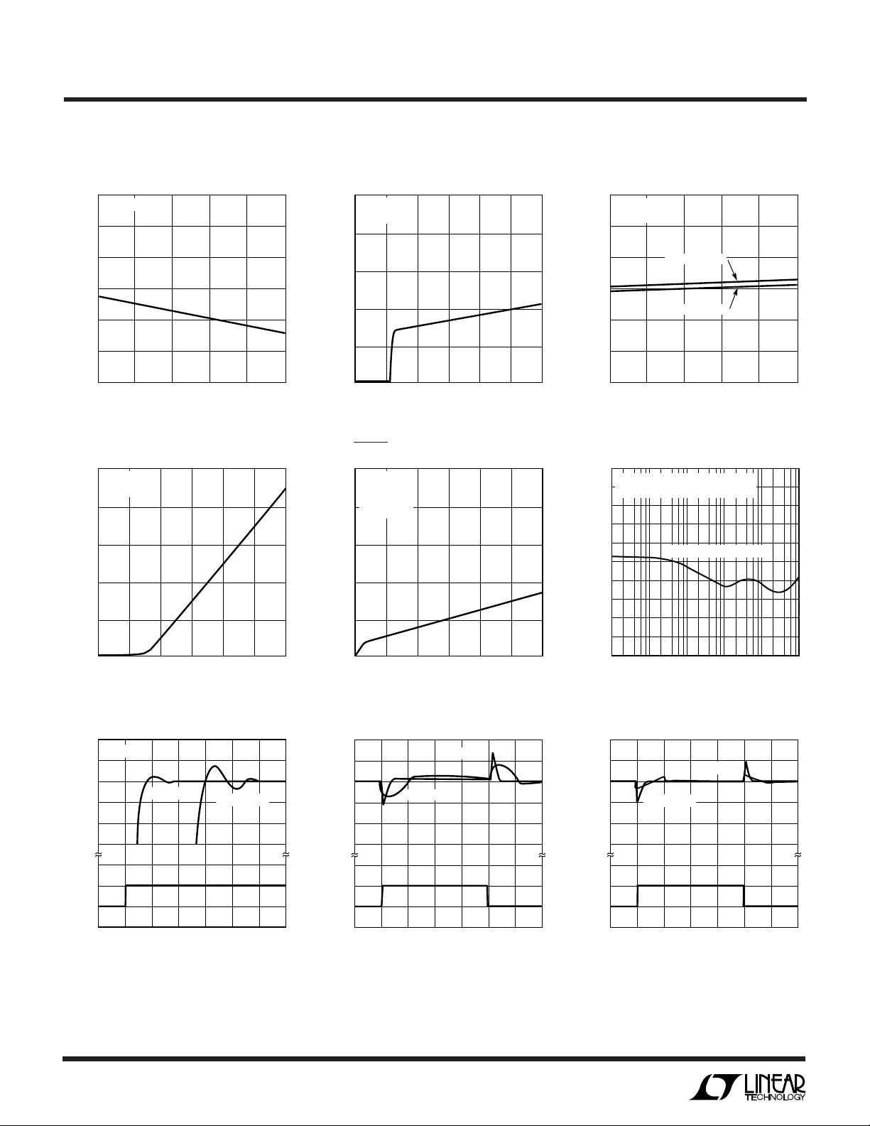
TYPICAL PERFORMANCE CHARACTERISTICS
3.0
VS = 15V
2.5
2.0
1.5
1.0
0.5
INPUT THRESHOLD VOLTAGE (V)
0
25 50 75 100
0
JUNCTION TEMPERATURE (°C)
VCC Sense Input Current
50
TJ = 25°C
V
= 15V
S
40
30
20
LT1312 G10
125
Enable Input CurrentEnable Input Threshold Voltage
50
TJ = 25°C
V
= 15V
S
40
30
20
ENABLE INPUT CURRENT (µA)
10
0
0
234
1
ENABLE INPUT VOLTAGE (V)
VALID Output Voltage
1.0
TJ = 25°C
V
= 15V
S
EN0 = 5V
0.8
EN1 = 0V
0.6
0.4
56
LT1312 G11
VCC Sense Threshold Voltage
5.5
TJ = 25°C
= 15V
V
S
5.0
4.5
4.0
3.5
SENSE THRESHOLD VOLTAGES (V)
3.0
CC
V
2.5
0
SWITCH TO 5V
SWITCH TO 3.3V
25 50 75 100
JUNCTION TEMPERATURE (°C)
Ripple Rejection (12V)
100
TJ = 25°C, 12V MODE
80
60
40
= 15V + 100mV
V
S
RIPPLE
RMS
C
= 1µF TANTALUM
OUT
125
LT1312 G12
SENSE INPUT CURRENT (µA)
CC
V
12.4
12.2
12.0
11.8
OUTPUT VOLTAGE (V)EN0 INPUT (V)
11.6
10
0
0
234
1
ENABLE INPUT VOLTAGE (V)
56
LT1312 G13
12V Turn-On Waveform
VS = 15V
C
= 1µF
OUT
5
0
–0.2 0 0.2 0.4 0.6 0.8 1.0 1.2
TIME (ms)
C
= 10µF
OUT
LT1312 G16
VALID OUTPUT VOLTAGE (V)
0.2
0
0
1.0 1.5 2.0
0.5
VALID OUTPUT CURRENT (mA)
Line Transient Response (12V)
40
20
0
–20
CHANGE (mV)
OUTPUT VOLTAGE
–40
15
SUPPLY
13
VOLTAGE (V)
–0.1 0 0.1 0.2 0.3 0.4 0.5 0.6
C
OUT
C
OUT
= 10µF
TIME (ms)
= 1µF
2.5 3.0
LT1312 G14
LT1312 G17
20
RIPPLE REJECTION RATIO (dB)
0
100 1k 10k 100k 1M
10
FREQUENCY (Hz)
Load Transient Response (12V)
LT1312 G15
4
Page 5

UUU
PIN FUNCTIONS
LT1312
Supply Pin: Power is supplied to the device through the
supply pin. The supply pin should be bypassed to ground
if the device is more than 6 inches away from the main
supply capacitor. A bypass capacitor in the range of 0.1µF
to 1µF is sufficient. The supply voltage to the LT1312 can
be loosely regulated between 13V and 20V. See Applications Information section for more detail.
VPP
Pin: This regulated output supplies power to the
OUT
PCMCIA card VPP pins which are typically tied together
at the card socket. The VPP
output is current limited
OUT
to approximately 330mA. Thermal shutdown provides a
second level of protection. A 1µF to 10µF tantalum output
capacitor is recommended. See Applications Information section for more detail on output capacitor considerations.
Input Enable Pins: The two digital input pins are high
impedance inputs with approximately 20µA input current
W
BLOCK DIAGRAM
at 2.4V. The input thresholds are compatible with CMOS
controllers and can be driven from either 5V or 3.3V
CMOS logic. ESD protection diodes limit input excursions
to 0.6V below ground.
VALID Output Pin: This pin is an open-collector NPN
output which is driven low when the VPP
pin is in
OUT
regulation, i.e., when it is above 11V. An external 51k pullup resistor is connected between this output and the same
5V or 3.3V logic supply powering the PCMCIA compatible
control logic.
VCC Sense Pin: A built-in comparator and 4V reference
automatically switches the VPP
from 5V to 3.3V de-
OUT
pending upon the voltage sensed at the PCMCIA card
socket VCC pin. The input current for this pin is approximately 30µA. For 5V only operation, connect the Sense pin
directly to ground. An ESD protection diode limits the
input voltage to 0.6V below ground.
V
S
V
CC
SENSE
EN0
EN1
+
–
4V
LOW DROPOUT
LINEAR
REGULATOR
VOLTAGE
LOGIC CONTROL
11V
VPP
OUT
VALID
+
–
LT1312 BD
5
Page 6

LT1312
U
OPERATION
The LT1312 is a programmable output voltage, lowdropout linear regulator designed specifically for PCMCIA
VPP drive applications. Input power is typically obtained
from a loosely regulated input supply between 13V and
20V (see Applications Information section for more detail
on the input power supply). The LT1312 consists of the
following blocks:
Low Dropout Voltage Linear Regulator: The heart of the
LT1312 is a PNP-based low-dropout voltage regulator
which drops the unregulated supply voltage from 13V to
20V down to 12V, 5V, 3.3V, 0V or Hi-Z depending upon the
state of the two Enable inputs and the VCC Sense input. The
regulator has built-in current limiting and thermal shutdown to protect the device, the load, and the socket
against inadvertent short circuiting to ground.
U
WUU
APPLICATIONS INFORMATION
The LT1312 is a voltage programmable linear regulator
designed specifically for PCMCIA VPP driver applications.
The device operates with very low quiescent current
(30µA) in the 0V and Hi-Z modes of operation. In the Hi-Z
mode, the output leakage current falls to 1µA. Unloaded
quiescent current rises to only 55µA and 75µA when
programmed to 3.3V and 5V respectively. In addition to
the low quiescent currents, the LT1312 incorporates several protection features which make it ideal for PCMCIA
applications. The LT1312 has built-in current limiting
(330mA) and thermal shutdown to protect the device and
the socket VPP pins against inadvertent short-circuit
conditions.
Voltage Control Logic: The LT1312 has five possible
output modes: 0V, 3.3V, 5V, 12V and Hi-Z. These five
modes are selected by the two Enable inputs and the V
Sense input as described by the Truth Table.
V
Sense Comparator: When the VCC mode is selected,
CC
the LT1312 automatically adjusts the regulated VPP output voltage to 3.3V or 5V depending upon the voltage
present at the PC card VCC supply pin. The threshold
voltage for the comparator is set at 4V and there is
approximately 50mV of hysteresis provided to ensure
clean switching between 3.3V and 5V.
VPP VALID Comparator: A voltage comparator monitors
the output voltage when the 12V mode is selected and is
driven low when the output is in regulation above 11V.
an auxiliary winding to the 5V inductor in a split 3.3V/5V
LTC1142HV power supply system. A turns ratio of 1:1.8 is
used for transformer T1 to ensure that the input voltage to
the LT1312 falls between 13V and 20V under all load
conditions. The 9V output from this additional winding is
rectified by diode D2, added to the main 5V output and
applied to the input of the LT1312. (Note that the auxiliary
winding must be phased properly as shown in Figure 1.)
The auxiliary winding is referenced to the 5V output which
provides DC current feedback from the auxiliary supply to
the main 5V section. The AC transient response is improved by returning the negative lead of C5 to the 5V
output as shown.
CC
AUXILIARY WINDING POWER SUPPLIES
Because the LT1312 provides excellent output regulation,
the input power supply may be loosely regulated. One
convenient (and economic) source of power is an auxiliary
winding on the main 5V switching regulator inductor in the
main system power supply.
LTC®1142HV Auxiliary Winding Power Supply
Figure 1 is a schematic diagram which describes how a
loosely regulated 14V power supply is created by adding
6
When the 12V output is activated by a TTL high on the
Enable line, the 5V section of the LTC1142HV is forced into
continuous mode operation. A resistor divider composed
of R2, R3 and switch Q3 forces an offset which is subtracted from the internal offset at the Sense– input (pin 14)
of the LTC1142HV. When this external offset cancels the
built-in 25mV offset, Burst Mode
and the LTC1142HV is forced into continuous mode
operation. (See the LTC1142HV data sheet for further
detail). In this mode, the 14V auxiliary supply can be
Burst Mode is a trademark of Linear Technology Corporation.
TM
operation is inhibited
Page 7

LT1312
U
WUU
APPLICATIONS INFORMATION
V
1/2 LTC1142HV
5V REG
EN0
EN1
VALID
PDRIVE
NDRIVE
SENSE
SENSE
V
IN
+
–
6.5V TO 18V
10
9
20
15
14
IN
Q1
Q2
R3
18k
Q3
VN7002
+
D3
MBRS130T3
R1
100Ω
C2
1000pF
R2
100Ω
*LPE-6562-A026 DALE (605) 665-9301
+
C1
68µF
MBRS140
R5
0.033Ω
C3
220µF
D1
22Ω
T1
1.8T
30µH*
R4
D2
MBRS140
C4
1000pF
14V AUXILIARY SUPPLY
+
C5
22µF
5V
OUTPUT
V
S
VPP
EN0
VALID SENSE
OUT
LT1312EN1
GND
TO CARD VPP PIN
0V, 3.3V, 5V, 12V OR HI-Z
+
FROM
PIN
CARD V
CC
LT1312 F1
1µF
Figure 1. Deriving 14V Power from an Auxiliary Winding on the LTC1142HV 5V Regulator
loaded without regard to the loading on the 5V output of
the LTC1142HV.
Continuous mode operation is only invoked when the
LT1312 is programmed to 12V. If the LT1312 is programmed to 0V, 3.3V or 5V, power is obtained directly
from the main power source (battery pack) through diode
D1. Again, the LT1312 output can be loaded without
regard to the loading of the main 5V output.
R4 and C4 absorb transient voltage spikes associated with
the leakage inductance inherent in T1's secondary winding
and ensure that the auxiliary supply does not exceed 20V.
Figure 2 is a graph of output voltage versus output current
for the auxiliary 14V supply shown in Figure 1. Note that
the auxiliary supply voltage is slightly higher when the 5V
output is heavily loaded. This is due to the increased
energy flowing through the main 5V inductor.
LTC1142 Auxiliary Power from the 3.3V Output
The circuit of Figure 1 can be modified for operation with
low-battery count applications (6 cell). As the input voltage falls, the 5V duty cycle increases to the point where
there is simply not enough time to transfer energy from the
5V primary to the auxiliary winding. For applications
where heavy 12V load currents exist in conjunction with
low input voltages (<6.5V), the auxiliary winding can be
derived from the 3.3V section instead of the 5V section of
the LTC1142. In this case, a transformer with a turns ratio
of 1:3.4 to 1:3.6 should be used in place of the 3.3V section
17
VIN = 8V
EN0 = HI
16
15
14
I
OUT5V
13
12
AUXILIARY OUTPUT VOLTAGE (V)
11
0.1
AUXILIARY OUTPUT CURRENT (mA)
Figure 2. LTC1142 Auxiliary Supply Voltage
= 0mA
I
= 1A
OUT5V
101 100 1000
LT1312 F2
7
Page 8

LT1312
U
WUU
APPLICATIONS INFORMATION
inductor as shown in Figure 3. MOSFET Q4 and diode D4
have been added and diode D1 is no longer used. In the
previous circuit, power is drawn directly from the batteries
through D1, when the LTC1142 is in Burst Mode operation
and the VPP pin requires 3.3V or 5V. For these lower input
voltages this technique is no longer valid as the input will
fall below the LT1312 regulator’s dropout voltage. To
correct for this situation, the additional switch Q4 forces
the switching regulator
whenever 3.3V, 5V or 12V
LINE POWERED SUPPLIES
In line operated products such as: desktop computers,
dedicated PC card readers/writers, medical equipment,
test and measurement equipment, etc., it is possible to
derive power from a relatively “raw” source such as a 5V
or 12V power supply. The 12V supply line in a desktop
computer however, is usually too “dirty” to apply directly
to the VPP pins of a PCMCIA card socket. Power supply
switching and load transients may create voltage spikes
into continuous mode operation
is selected.
on this line that may damage sensitive PCMCIA flash
memory cards if applied directly to the VPP pins.
Flash Memory Card VPP Power Considerations
PCMCIA compatible flash memory cards require tight
regulation of the 12V VPP programming supply to ensure
that the internal flash memory circuits are never subjected
to damaging conditions. Flash memory circuits are typically rated with an absolute maximum of 13.5V and VPP
must be maintained at 12V ±5% under all possible load
conditions during erase and program cycles. Undervoltage
can decrease specified flash memory reliability and overvoltage can damage the device1.
Generating 14V from 5V or 12V
It is important that the 12V VPP supply for the two VPP
lines to the card be free of voltage spikes. There should be
little or no overshoot during transitions to and from the
12V level.
1
See Application Note AP-357, “Power Supply Solutions for Flash Memory,”
Intel Corporation, 1992.
1/2 LTC1142
3.3V REG
EN0
EN1
VALID
V
PDRIVE
NDRIVE
SENSE
SENSE
Q4
VN7002
V
IN
5.4V TO 12V
24
IN
23
6
1
+
28
–
+
C1
68µF
Q1
D3
Q2
MBRS130T3
R1
100Ω
C2
1000pF
R3
18k
Q3
VN7002
R2
100Ω
+
*LPE-6582-A086 DALE (605) 665-9301
MBRS1100
T1
3.38T
22µH*
R4
0.033Ω
C3
220µF
R4
22Ω
D2
C4
1000pF
D4
18V
14V AUXILIARY SUPPLY
+
C5
22µF
3.3V
OUTPUT
Figure 3. Deriving Auxiliary 14V Power from an LTC1142 3.3V Regulator
V
S
EN0
VPP
OUT
LT1312EN1
VALID SENSE
GND
TO CARD VPP PIN
0V, 3.3V, 5V, 12V OR Hi-Z
+
1µF
FROM CARD
PIN
V
CC
LT1312 F3
8
Page 9

LT1312
V
S
EN0 VPP
OUT
LT1312
EN1
VALID SENSE
GND
+
>1µF TANTALUM
OR ALUMINUM
LT1312 F6
0.1µF
13V TO 20V
U
WUU
APPLICATIONS INFORMATION
1N5158
4
2
FB
1
1k
1µF
31
8
4
12V
5
V
IN
LT1172
3
100µH
V
SW
C
5V
+
22µF
GND V
+
Figure 4. Local 5V to 15V Boost Regulator for Line Operated Applications
100µH
+
22µF
100Ω
2
V
IN
LIM
LT1111CS8
SENSE
GND SW2
5
SW1I
1N5158
10k
1%
1k
1%
100k
1%
10k
1%
13.75V
+
100µF
V
S
EN0 VPP
VALID SENSE
13.75V
OUT
LT1312EN1
GND
+
LT1312 F4
TO CARD VPP PIN
0V, 5V, 12V OR HI-Z
1µF
+
100µF
V
S
EN0 VPP
EN1
VALID SENSE
OUT
LT1312
GND
+
LT1312 F5
TO CARD VPP PIN
0V, 5V, 12V OR HI-Z
1µF
Figure 5. Local 12V to 15V Boost Regulator for Line Operated Applications
This is easily accomplished by generating a local 14V
supply from a relatively “dirty” 5V or 12V supply as shown
in Figures 4 and 5. Precise voltage control (and further
filtering) is provided by the LT1312 driver/regulator. A
further advantage to this scheme is that it adds current
limit in series with the VPP pins to eliminate possible
damage to the card socket, the PC card, or the switching
power supply in the event of an accidental short circuit.
Output Capacitance
The LT1312 is designed to be stable with a wide range of
output capacitors. The minimum recommended value is a
1µF with an ESR of 3Ω or less. The capacitor is connected
directly between the output pin and ground as shown in
Figure 6.
For applications where space is very limited, capacitors as
low as 0.33µF can be used. Extremely low ESR ceramic
capacitors with values less than 1µF must have a 2Ω
resistor added in series with the output capacitor as shown
in shown in Figure 7.
Figure 6. Recommended >1µF Tantalum Output Capacitor
13V TO 20V
0.1µF
V
S
EN0 VPP
EN1
VALID SENSE
OUT
LT1312
GND
2Ω
0.33µF
CERAMIC
LT1312 F7
Figure 7. Using a 0.33µF to 1µF Output Capacitor
9
Page 10

LT1312
U
WUU
APPLICATIONS INFORMATION
Transient and Switching Performance
The LT1312 is designed to produce minimal overshoot with
capacitors in the range of 1µF to 10µF. Larger capacitor
values can be used with a slowing of rise and fall times.
The positive output slew rate is determined by the 330mA
current limit and the output capacitor. The rise time for a
0V to 12V transition is approximately 40µs, the rise time
for a 10µF capacitor is roughly 400µs (see the Transient
Response curves in the Typical Performance Characteristics section).
The fall time from 12V to 0V is set by the output capacitor
and an internal pull-down current source which sinks
about 30mA. This source will fully discharge a 1µF capaci-
tor in less than 1ms.
Thermal Considerations
Power dissipated by the device is the sum of two components: output current multiplied by the input-output differential voltage I
multiplied by supply voltage I
The ground pin current can be found by examining the
Ground Pin Current curves in the Typical Performance
Characteristics section.
Heat sinking, for surface mounted devices, is accomplished by using the heat spreading capabilities of the PC
board and its copper traces.
The junction temperature of the LT1312 must be limited to
125°C to ensure proper operation. Use Table 1 in conjunction with the typical performance graphs, to calculate the
power dissipation and die temperature for a particular
application and ensure that the die temperature does not
exceed 125°C under any operating conditions.
OUT
× (V
IN
– V
), and ground pin current
OUT
× VIN.
GND
Table 1. S8 Package*
COPPER AREA THERMAL RESISTANCE
TOPSIDE BACKSIDE BOARD AREA (JUNCTION-TO-AMBIENT)
2500 sq mm 2500 sq mm 2500 sq mm 120°C/W
1000 sq mm 2500 sq mm 2500 sq mm 120°C/W
225 sq mm 2500 sq mm 2500 sq mm 125°C/W
1000 sq mm 1000 sq mm 1000 sq mm 131°C/W
*Device is mounted topside.
Calculating Junction Temperature
Example: given an output voltage of 12V, an input supply
voltage of 14V, an output current of 100mA, and a
maximum ambient temperature of 50°C, what will the
maximum junction temperature be?
Power dissipated by the device will be equal to:
I
× (VS – VPP
OUT
OUT
) + (I
GND
× VIN)
where:
I
= 100mA
OUT
VIN = 14V
I
GND
at (I
= 100mA, VIN = 14V) = 5mA
OUT
so,
PD = 100mA × (14V – 12V) + (5mA × 15V) = 0.275W
Using Table 1, the thermal resistance will be in the range
of 120°C/W to 131°C/W depending upon the copper area.
So the junction temperature rise above ambient will be
less than or equal to:
0.275W × 131°C/W = 36°C
The maximum junction temperature will then be equal to
the junction temperature rise above ambient plus the
maximum ambient temperature or:
10
T
= 50°C + 36°C = 86°C.
JMAX
Page 11

U
TYPICAL APPLICATIONS
V
LOGIC
LT1312
Single Slot Interface to CL-PD6710
13V TO 20V
V
CC
A_VPP_PGM
A_VPP_V
VPP_VALID
CIRRUS LOGIC
CL-PD6710
A_V
A_V
51K
CC
5V
_5
CC
_3
CC
Si9430DY OR
MMSF3P02HD
3.3V
V
S
EN0
VPP
LT1312
EN1
VALID
GND
Si9933DY OR
MMDF2P01HD
OUT
SENSE
Single Slot Interface to “365” Type Controller
+
3.3V OR 5V
1µF
VPP1
VPP2
PCMCIA
CARD SLOT
V
CC
+
10µF
LT1312 TA2
V
LOGIC
V
CC
A_VPP_EN0
A_VPP_EN1
“365” TYPE
CONTROLLER
A_V
CC
A_V
CC
A:GPI
_EN0
_EN1
51k
5V
IN1
LTC1157CS8
IN2
GND
13V TO 20V
V
S
EN0
VPP
OUT
EN1
LT1312
SENSE
VALID
GND
V
S
G1
Si9410DY OR
MMSF5N02HD
3.3V OR 5V
+
1µF
VPP1
VPP2
CARD SLOT
V
CC
PCMCIA
+
G2
Si9956DY OR
MMDF3N02HD
3.3V
10µF
LT1312 TA3
Information furnished by Linear Technology Corporation is believed to be accurate and reliable.
However, no responsibility is assumed for its use. Linear Technology Corporation makes no representation that the interconnection of its circuits as described herein will not infringe on existing patent rights.
11
Page 12

LT1312
PACKAGE DESCRIPTION
U
Dimensions in inches (millimeters) unless otherwise noted.
S8 Package
8-Lead Plastic SOIC
0.189 – 0.197*
(4.801 – 5.004)
7
8
5
6
0.228 – 0.244
(5.791 – 6.197)
0.010 – 0.020
(0.254 – 0.508)
0.008 – 0.010
(0.203 – 0.254)
*THESE DIMENSIONS DO NOT INCLUDE MOLD FLASH OR PROTRUSIONS.
MOLD FLASH OR PROTRUSIONS SHALL NOT EXCEED 0.006 INCH (0.15mm).
× 45°
0.016 – 0.050
0.406 – 1.270
0.053 – 0.069
(1.346 – 1.752)
0°– 8° TYP
0.014 – 0.019
(0.355 – 0.483)
RELATED PARTS
See PCMCIA Product Family table on the first page of this data sheet.
0.150 – 0.157*
(3.810 – 3.988)
1
3
2
4
(0.101 – 0.254)
0.050
(1.270)
BSC
0.004 – 0.010
SO8 0294
12
Linear Technology Corporation
1630 McCarthy Blvd., Milpitas, CA 95035-7487
(408) 432-1900
●
FAX
: (408) 434-0507
●
TELEX
: 499-3977
LT/GP 0894 10K • PRINTED IN USA
LINEAR TECHNOLOGY CORPORATION 1994
 Loading...