

Page 1
LT1309
, LTC and LT are registered trademarks of Linear Technology Corporation.
500kHz Micropower
DC/DC Converter
for Flash Memory
EATU
F
■
60mA Output Current at 12V from 3V or 5V Supply
■
Shutdown to 9µA
■
VPP VALID Comparator
■
Up to 85% Efficiency
■
Switching Frequency: 500kHz (Typical)
■
Quiescent Current: 650µA
■
Low V
■
Soft Start Reduces Supply Current Transients
■
Uses Low Value, Small Size,
S
RE
Switch: 300mV at 0.5A (Typical)
CESAT
Surface Mount Inductors
■
Available in 8-Lead SO Package
U
O
PPLICATI
A
■
Flash Memory VPP Generators
■
Type II and III PCMCIA Card DC/DC Converters
■
3V to 12V, 5V to 12V Converters
■
Portable Computers and Instruments
■
Cellular Telephones
■
DC/DC Converter Module Replacements
S
DUESCRIPTIO
The LT®1309 is a 500kHz micropower DC/DC converter
for Flash Memory. The regulator features Burst Mode
operation with a 0.5A, 300mV switch, enabling 85%
efficiency at the fixed 12V output. High frequency operation permits the use of small value, and therefore small
size, surface mount inductors and capacitors. The LT1309
comes in an 8-lead SO package allowing extremely
compact PC board layouts. These features make the
device attractive for PCMCIA cards, cellular phones and
other applications where PC board space is limited.
Quiescent current is 650µA decreasing to 9µA when the
part shuts down. The device includes a soft start feature
which limits supply current transients during turn-on.
The LT1309 contains a VPP VALID comparator with a
logic output that goes low when the output voltage is
ready to program 12V Flash Memory. This comparator
simplifies the interface to external control logic.
Burst Mode is a trademark of Linear Technology Corporation.
TM
A
PPLICATITYPICAL
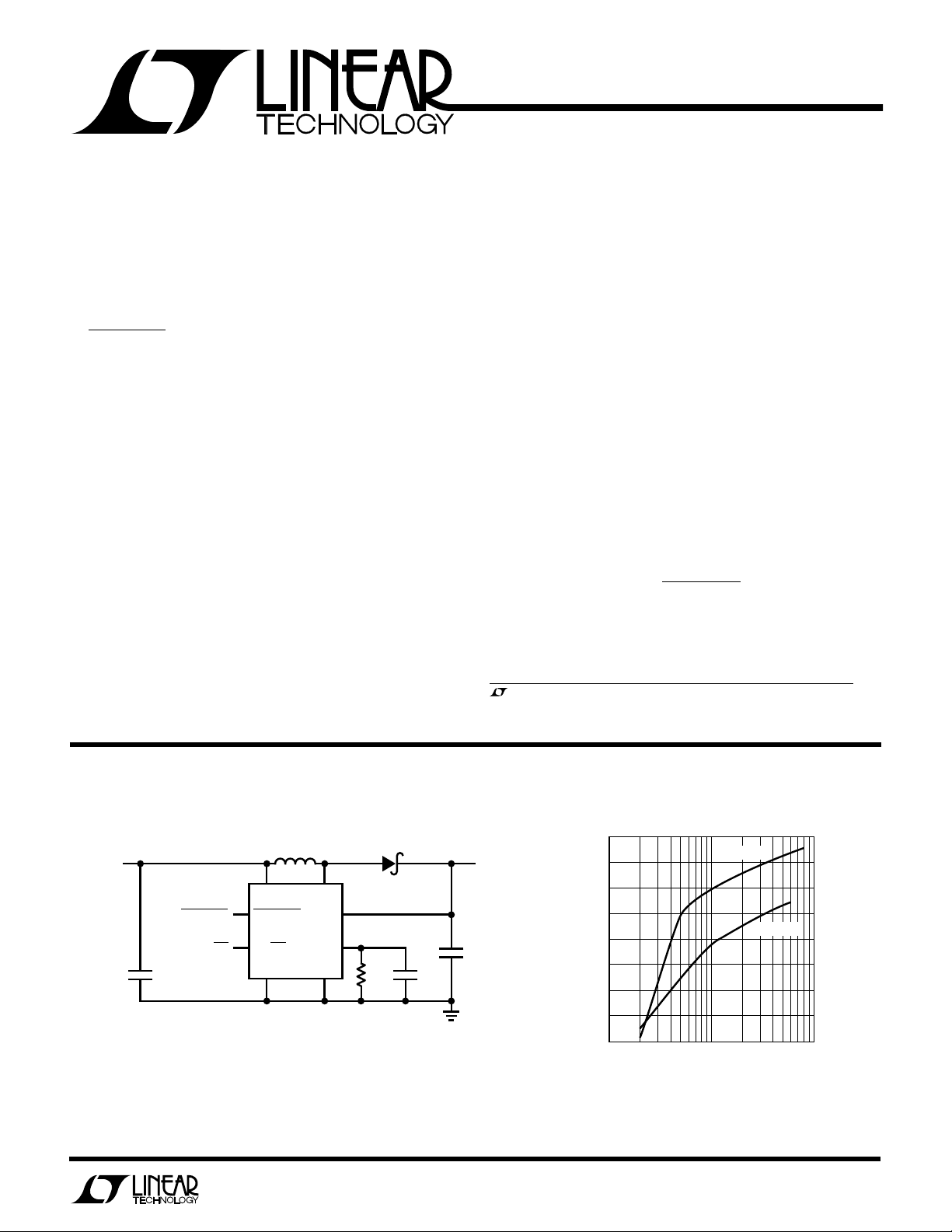
12V, 60mA Flash Memory Programming Supply 12V Output Efficiency
L1*
V
IN
3.3V TO 5V
VPP VALID
+
*
**
†
ON/OFF
C1
4.7µF
MURATA ERIE LQH3C100K0YM00
CERAMIC
MOTOROLA MBR0530
10µH
V
IN
VPP VALID
LT1309
ON/OFF
PGND GND
O
V
SENSE
SOFT
START
U
SW
R1
1M
D1
†
VPP 12V, 60mA
C3
0.1µF
LT1309 • TA01
C2
1µF**
86
84
82
80
78
76
EFFICIENCY (%)
74
72
70
1
VIN = 5V
VIN = 3.3V
10 100
LOAD CURRENT (mA)
LT1309 • TA02
1
Page 2
LT13 09
WU
U
PACKAGE
/
O
RDER I FOR ATIO
W
O
A
LUTEXI T
S
VCC Voltage............................................................... 7V
VSW Voltage............................................................ 20V
V
V
V
I
Voltage ....................................................... 20V
SENSE
Voltage......................................................... 7V
ON/OFF
Voltage ............................................................. 7V
SEL
Voltage .............................................................. 7V
LIM
Maximum Power Dissipation ............................ 500mW
Operating Temperature Range .....................0°C to 70°C
Storage Temperature Range ................. –65°C to 150°C
A
WUW
ARB
U
G
I
S
SOFT START
V
PGND
V
TOP VIEW
1
2
CC
3
4
SW
S8 PACKAGE
8-LEAD PLASTIC SO
T
= 150°C, θJA = 150°C/W
JMAX
8
7
6
5
ON/OFF
SENSE
VPP VALID
GND
ORDER PART
NUMBER
LT1309CS8
S8 PART MARKING
1309
Lead Temperature (Soldering, 10 sec)..................300°C
Consult factory for Industrial and Military grade parts.
LECTRICAL C CHARA TERIST
E
SYMBOL PARAMETER CONDITIONS MIN TYP MAX UNITS
I
Q
f
OSC
DC Maximum Duty Cycle ● 80 85 92 %
t
ON
V
CESAT
Quiescent Current V
Quiescent Current, Shutdown V
Input Voltage Range 2 6 V
Output Sense Voltage ● 11.5 12 12.6 V
Output Referred Comparator Hysteresis 35 mV
Oscillator Frequency Current Limit Not Asserted 400 500 700 kHz
Switch ON Time 1.7 µs
Reference Line Regulation 2V < VIN < 6V 0.06 0.15 %/V
Switch Saturation Voltage ISW = 0.5A 230 350 mV
Switch Leakage Current VSW = 12V, Switch Off 0.1 10 µA
Switch Current Limit VIN = 5V, Soft Start Floating 400 600 900 mA
Soft Start Current Soft Start Grounded 80 120 µA
ON/OFF Input Voltage Low 0.8 V
ON/OFF Input Voltage High 1.6 V
ON/OFF Bias Current V
Sense Pin Input Current 50.0 90 µA
VPP VALID Threshold V
VPP VALID Output Voltage Low I
VPP VALID Output Voltage High I
ICS
TA = 25°C, VCC = 5V, V
= 12V 650 900 µA
SENSE
= 0.2V 9 15 µA
ON/OFF
= 3V, Soft Start Floating 450 650 950 mA
V
IN
= 5V 16.0 24.0 µA
ON/OFF
= 3V 8.0 14.0 µA
V
ON/OFF
= 0V 0.1 1.0 µA
V
ON/OFF
= 0.2V 0.1 1 µA
V
ON/OFF
Rising (High to Low Transition) V
SENSE
= 100µA 0.13 0.3 V
SINK
= 2.5µA 4 4.5 V
SOURCE
= 3V, unless otherwise noted.
ON/OFF
SENSE
– 200mV
The ● denotes specifications which apply over the full operating
temperature range.
2
Page 3
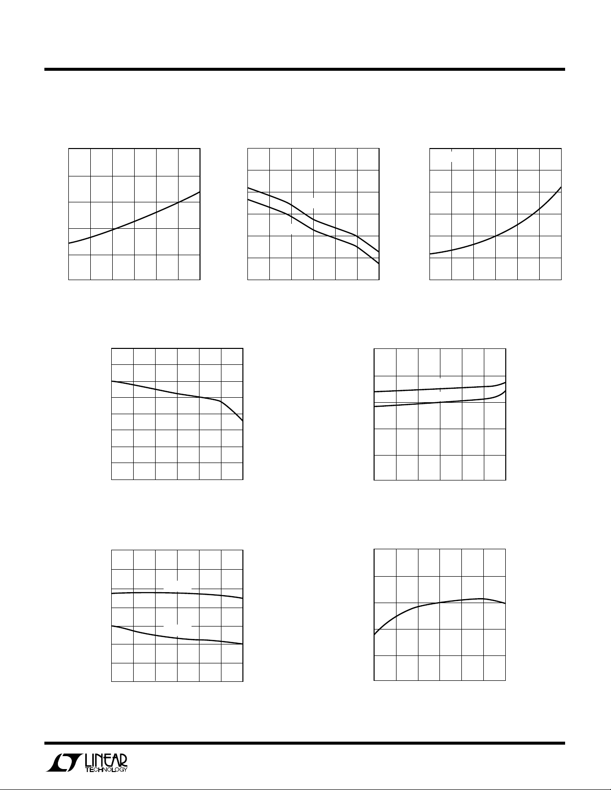
W
TEMPERATURE (°C)
–50
100
SWITCH SATURATION VOLTAGE (mV)
125
150
175
200
250
–25
02550
1309 G03
75 100
225
ISW = 500mA
TEMPERATURE (°C)
–50
300
SUPPLY CURRENT (µA)
400
500
600
700
800
–25
02550
1309 G05
75 100
VCC = 5V
V
CC
= 3V
U
TYPICAL PERFORMANCE CHARACTERISTICS
LT1309
Oscillator Frequency
800
700
600
500
400
OSCILLATOR FREQUENCY (kHz)
300
–50
02550
–25
TEMPERATURE (°C)
Sense Voltage
12.20
12.15
12.10
12.05
12.00
11.95
SENSE VOLTAGE (V)
11.90
11.85
11.80
–25 0 50
–50
75 100
1309 G01
25
TEMPERATURE (°C)
Switch Current Limit
1000
900
800
700
600
SWITCH CURRENT (mA)
500
400
–50
–25
75
100
1309 G04
VCC = 3V
VCC = 5V
02550
TEMPERATURE (°C)
Switch Saturation Voltage
75 100
1309 G02
Supply Current
14
12
10
8
SUPPLY CURRENT (µA)
6
4
2
0
–50
Supply Current in Shutdown
VCC = 5V
VCC = 3V
50 100
–25 0
25 75
TEMPERATURE (°C)
1309 G06
Maximum Duty Cycle
95
90
85
80
MAXIMUM DUTY CYCLE (%)
75
70
–50
02550
–25
TEMPERATURE (°C)
75 100
1309 G07
3
Page 4

LT13 09
W
U
TYPICAL PERFORMANCE CHARACTERISTICS
12V
V
OUT
2V/DIV
VPP VALID
10V/DIV
V
ON/OFF
10V/DIV
Start-Up Waveforms, I
50µs/DIV 1309 G08
= 1mA
LOAD
12V OUTPUT
AC COUPLED
I
LOAD
Load Transient Response,
C
OUT
1V/DIV
60mA
10mA
50µs/DIV 1309 G10
= 1µF
V
OUT
5V/DIV
500mA/DIV
V
ON/OFF
10V/DIV
Start-Up Waveforms, I
I
L
50µs/DIV 1309 G09
LOAD
= 10mA
UU U
PI FU CTIO S
SOFT START (Pin 1): A 0.1µ F/1MΩ parallel RC from this
pin to GND provides a Soft Start function upon device
turn-on. Initially about 80µ A will flow from the pin into the
capacitor. When the voltage at the pin reaches approximately 0.4V, current ceases flowing out of the pin.
V
(Pin 2): Input Supply. At least 1µF input bypass
CC
capacitance is required. More capacitance reduces ringing on the supply line.
PGND (Pin 3): Power Ground. Connect to ground plane.
VSW (Pin 4): Collector of Power Switch. High dV/dt
present on this pin. To minimize radiated noise keep
layout short and direct.
GND (Pin 5): Signal Ground. Connect to ground plane.
VPP VALID (Pin 6): This pin provides a logic signal
indicating that output voltage has reached 12V. Active low
with internal 200k pull-up resistor.
SENSE (Pin 7): Output Sense Pin. This pin connects to a
resistive divider that sets the output voltage. In shutdown,
the resistor string is disconnected and current into this pin
reduces to < 1µA.
ON/OFF (Pin 8): Shutdown Control. When pulled below
1.5V, this pin disables the LT1309 and reduces supply
current to 9µ A. All circuitry is disabled in shutdown. The
part is enabled when ON/OFF is greater than 1.5V.
4
Page 5

BLOCK DIAGRA
7
864k
4k
100k
W
ON/OFFSENSE
8
POWER ON
–
C2
+
–
C1
+
LT1309
V
CC
R2
700Ω
BIAS
2
R1
3Ω
SW
4
Q2
× 1
Q1
× 50
36mV
+
–
+
V
CC
200k
VPP VALID
6
OFF
500kHz
OSCILLATOR
C3
–
Q3
1
SOFT START
V
1.24V
REF
U
OPERATIO
The LT1309 is a current limited, Burst Mode (gated
oscillator) type switching regulator that produces a 12V
output from a 3.3V or 5V input. Operation can best be
understood by referring to the Block Diagram. When the
voltage at the Sense pin (Pin 7) is less than 12V, comparator C1 enables the oscillator, turning switches Q1 and Q2
on. The switch turns off when current limit is reached or
when the oscillator maximum on-time is reached. When
5 3
GND
PGND
1309 BD
Q2 turns off, current built up in the inductor flows into the
output capacitor and load. This action occurs until the
output voltage reaches 12V. During start-up, the Sense pin
voltage is either 3.3V or 5V, depending on the input. The
VPP VALID signal remains high until the output voltage
reaches 12V, signaling correct voltage level to program
flash memory. Connecting a 1µF/0.1µF parallel RC to the
Soft Start pin limits inrush current during start-up.
5
Page 6

LT13 09
U
WUU
APPLICATIONS INFORMATION
Inductor Selection
The low inductance value required with the LT1309 (10µH)
allows the use of very small units such as the Murata-Erie
LQH3C100. Requirements for the inductor include low
DCR, ability to perform efficiently at 500kHz and a saturation current rating of 700mA to 900mA. Often inductor
manufacturers rate maximum current for a small inductor
based on self-heating considerations. For use in switching
regulators where the inductor current is not constant the
maximum specified DC current can be safely exceeded.
Capacitor Selection
The LT1309 needs very little input and output capacitance
to function. Output capacitance should be 1µF or 2µF for
acceptable output ripple voltage. Flash memory tolerates
higher ripple voltage than might be suitable for a low noise
system. The capacitor can be either a single high capacitance ceramic unit such as Tokin 1E105ZY5U-203 or
Murata-Erie GRM230Y5V105Z016, or can be distributed
as 10 to 20 0.1µF ceramic units. Lower ripple can be
obtained by increasing the capacitance to the 5µ F to 10µ F
level. 2µF to 5µF of tantalum (low-Q) capacitance is
recommended on the input side to reduce resonance
effects which can otherwise cause hundreds of millivolts
of ripple voltage at the input.
Diode Selection
The LT1309’s high switching speed demands a high speed
rectifier. Schottky diodes are preferred for their low forward drop and fast recovery. A suitable choice is the
Motorola MBR0520. This is a 0.5A, 20V Schottky in a very
small package that is 1.35mm high.
PC Board Layout
The component placement shown in Figure 1 is recommended for PC board layouts. The high speed current
paths are kept to a minimum distance and the switch node
copper is minimized to keep radiated noise low. Notice the
placement of the input decoupling capacitor next to the IC.
This is necessary for best performance.
R1
C3
1
C1
V
IN
L1
D1
V
OUT
Figure 1. LT1309 Recommended Layout
2
3
4
C2
GND
8
7
6
VPP VALID
5
ON/OFF
1309 F01
6
Page 7

PACKAGE DESCRIPTION
U
Dimensions in inches (millimeters) unless otherwise noted.
S8 Package
8-Lead Plastic Small Outline (Narrow 0.150)
(LTC DWG # 05-08-1610)
0.189 – 0.197*
(4.801 – 5.004)
7
8
5
6
LT1309
0.010 – 0.020
(0.254 – 0.508)
0.008 – 0.010
(0.203 – 0.254)
*
DIMENSION DOES NOT INCLUDE MOLD FLASH. MOLD FLASH
SHALL NOT EXCEED 0.006" (0.152mm) PER SIDE
**
DIMENSION DOES NOT INCLUDE INTERLEAD FLASH. INTERLEAD
FLASH SHALL NOT EXCEED 0.010" (0.254mm) PER SIDE
× 45°
0°– 8° TYP
0.016 – 0.050
0.406 – 1.270
0.228 – 0.244
(5.791 – 6.197)
0.053 – 0.069
(1.346 – 1.752)
0.014 – 0.019
(0.355 – 0.483)
0.150 – 0.157**
(3.810 – 3.988)
1
3
2
4
(1.270)
0.004 – 0.010
(0.101 – 0.254)
0.050
BSC
SO8 0695
Information furnished by Linear Technology Corporation is believed to be accurate and reliable.
However, no responsibility is assumed for its use. Linear Technology Corporation makes no representation that the interconnection of its circuits as described herein will not infringe on existing patent rights.
7
Page 8

LT13 09
RELATED PARTS
PART NUMBER DESCRIPTION COMMENTS
LT1106 Micropower Step-Up DC/DC Converter, 12V at 60mA Thin TSSOP Package for Type I PCMCIA Card
LT1109-12 Micropower Step-Up DC/DC Converter, 12V at 60mA Flash Memory VPP Generator, Adjustable Also
LT1109A-12 Micropower Step-Up DC/DC Converter, 12V at 120mA VPP Generator, Adjustable Also
LTC®1262 Inductorless Flash Memory Programming Supply, 12V at 30mA Switched Capacitor Converter, No Inductor
LT1303 Micropower High Efficiency DC/DC Converter with Low-Battery Detector Adjustable and Fixed 5V, I
up to 200mA
OUT
8
Linear Technology Corporation
1630 McCarthy Blvd., Milpitas, CA 95035-7417
(408) 432-1900
●
FAX
: (408) 434-0507
●
TELEX
: 499-3977
LT/GP 0896 7K • PRINTED IN THE USA
LINEAR TECHNOLOGY CORPORATION 1995
 Loading...