

Page 1
Final Electrical Specifications
FEATURES
LOAD CURRENT (mA)
1
EFFICIENCY (%)
95
90
85
80
75
70
65
10 100 1000
1308 F01a
VIN = 4.2V
VIN = 3.6V
VIN = 3V
LT1308
Single Cell High Current
Micropower 600kHz
Boost DC/DC Converter
January 1998
U
DESCRIPTION
■
5V at 1A from a Single Li-Ion Cell
■
3.3V at 300mA from a Single NiCd Cell
■
Low Quiescent Current: 100µA
■
Operates with VIN as Low as 1V
■
Fixed Frequency Operation: 600kHz
■
Current Mode PWM Delivers Low Output Ripple
■
Guaranteed Start-Up into Full Load
■
Low Shutdown Current: 3µA
■
Low-Battery Comparator
■
Automatic Burst ModeTM Operation at Light Load
■
Low V
Switch: 300mV at 2A
CESAT
U
APPLICATIONS
■
GSM Terminals
■
Digital Cameras
■
Answer-Back Pagers
■
Cordless Telephones
■
DECT Phones
■
GPS Receivers
■
Battery Backup Supplies
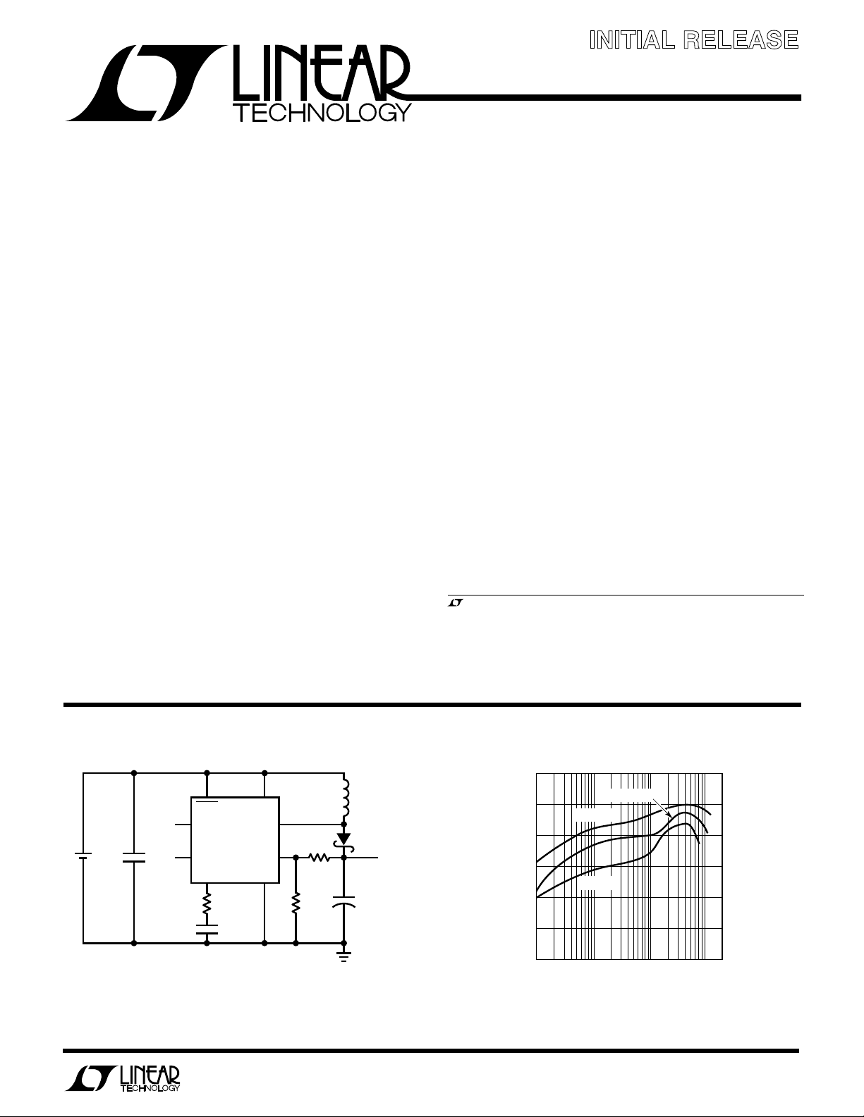
The LT®1308 is a micropower, fixed frequency boost
DC/DC converter that operates from an input voltage as
low as 1V. Capable of delivering 5V at load current of 1A
from a single Li-Ion cell, the LT1308 also features power
saving Burst Mode operation at light loads. High efficiency
is maintained over a broad 1mA to 1A load range.
The device contains a low-battery detector with a 200mV
reference and shuts down to less than 5µA quiescent
current. No-load quiescent current is 100µA and the
internal NPN power switch handles a 2A current with a
voltage drop of just 300mV.
High frequency 600kHz switching allows the use of small,
surface mount components. The LT1308’s current mode
architecture provides fast response to load and line variations. The device is available in an 8-lead SO package.
, LTC and LT are registered trademarks of Linear Technology Corporation.
Burst Mode is a trademark of Linear Technology Corporation.
TYPICAL APPLICATION
4.2V TO 3V
SHDN
LBI
Li-Ion
CELL
C1: CERAMIC
C2: AVX TPS SERIES
D1:INTERNATIONAL RECTIFIER 10BQ015
L1: COILTRONICS CTX5-1
COILCRAFT DO3316-472
Figure 1. Single Li-Ion Cell to 5V/1A DC/DC Converter
C1
10µF
LBO
U
L1
V
IN
SW
LT1308
FB
V
C
GND
R
C
47k
C
C
22nF
Information furnished by Linear Technology Corporation is believed to be accurate and reliable.
However, no responsibility is assumed for its use. Linear Technology Corporation makes no representation that the interconnection of its circuits as described herein will not infringe on existing patent rights.
301k
R2
100k
4.7µH
R1
D1
5V
1A
+
C2
100µF
1308F01
Converter Efficiency
1
Page 2
LT1308
WU
NUMBER
LT1308CS8
LT1308IS8
1308
1308I
A
W
O
LUTEXI T
S
A
WUW
ARB
U
G
I
S
VIN, SHDN, LBO Voltage ......................................... 10V
SW Voltage ............................................................. 30V
FB Voltage ....................................................... VIN + 1V
VC Voltage ................................................................ 2V
LBI Voltage ............................................ 0V ≤ V
LBI
≤ 1V
Current into FB Pin .............................................. ±1mA
Junction Temperature........................................... 125°C
Operating Temperature Range
Commercial (Note 1) ......................... –20°C to 70°C
PACKAGE
TOP VIEW
V
1
C
FB
2
SHDN
3
GND
4
S8 PACKAGE
8-LEAD PLASTIC SO
T
= 125°C, θJA = 80°C/W
JMAX
/
O
RDER I FOR ATIO
ORDER PART
LBO
8
LBI
7
V
6
IN
SW
5
S8 PART MARKING
Industrial ........................................... –40°C to 85°C
Storage Temperature Range ................ – 65°C to 150°C
Consult factory for Military grade parts.
Lead Temperature (Soldering, 10 sec)................. 300°C
LECTRICAL C CHARA TERIST
E
Commercial Grade 0°C to 70°C. VIN = 1.1V, V
SYMBOL PARAMETER CONDITIONS MIN TYP MAX UNITS
I
Q
VFBFeedback Voltage ● 1.20 1.22 1.24 V
I
B
g
m
A
V
f
OSC
Quiescent Current Not Switching ● 80 160 µA
FB Pin Bias Current (Note 2) VFB = V
Reference Line Regulation 1.1V ≤ VIN ≤ 2V (25°C, 0°C) 0.6 1.1 %/V
Minimum Input Voltage 0.92 1 V
Input Voltage Range ● 16V
Error Amp Transconductance ∆I = 5µA40µmhos
Error Amp Voltage Gain 25°C, 0°C 100 V/V
Switching Frequency ● 500 600 700 kHz
Maximum Duty Cycle ● 80 88 95 %
Switch Current Limit (Note 3) DC = 40% ● 2.0 2.5 A
Switch V
CESAT
Burst Mode Operation Switch Current Limit L = 3.3µH, V
Shutdown Pin Current V
LBI Threshold Voltage ● 180 200 220 mV
LBO Output Low I
LBO Leakage Current V
LBI Input Bias Current (Note 4) V
ICS
= VIN, TA = 25°C, unless otherwise noted.
SHDN
= 0V ● 13µA
V
SHDN
REF
1.1V ≤ V
2V ≤ V
70°C 80 V/V
DC = 80% 1.6 2 A
ISW = 2A (25°C, 0°C) 300 350 mV
I
SW
SHDN
V
SHDN
V
SHDN
SINK
LBI
LBI
≤ 2V (70°C) 1.5 %/V
IN
≤ 6V ● 0.3 0.8 %/V
IN
= 2A (70°C) 330 400 mV
= 3.3V, VIN = 1.2V 200 mA
OUT
= 1.1V ● 2.5 4.0 µA
= 6V 13 26 µA
= 0V ● –1.5 –2.5 µA
= 10µA ● 0.1 0.25 V
= 250mV, V
= 150mV ● 530nA
= 5V ● 0.01 0.1 µA
LBO
● 27 80 nA
U
2
Page 3
LT1308
LECTRICAL C CHARA TERIST
E
Commercial Grade 0°C to 70°C. VIN = 1.1V, V
SYMBOL PARAMETER CONDITIONS MIN TYP MAX UNITS
Low-Battery Detector Gain 1MΩ Load (25°C, 0°C) 1000 3000 V/V
Switch Leakage Current VSW = 5V ● 0.01 10 µA
Reverse Battery Current (Note 5) 750 mA
ICS
= VIN, TA = 25°C unless otherwise noted.
SHDN
1MΩ Load (70°C) 500 V/V
Commercial Grade TA = –20°C, VIN = 1.1V, V
SYMBOL PARAMETER CONDITIONS MIN TYP MAX UNITS
I
V
g
A
f
Q
FB
m
V
OSC
Quiescent Current VFB = 1.3V, Not Switching 80 160 µA
Feedback Voltage 1.195 1.22 1.245 V
Error Amp Transconductance ∆I = 5µA35µmhos
Error Amp Voltage Gain 100 V/V
Switching Frequency 500 600 750 kHz
Maximum Duty Cycle 88 %
Switch V
CESAT
Shutdown Pin Current V
LBI Threshold Voltage 180 200 220 mV
Industrial Grade –40°C to 85°C. VIN = 1.2V, V
SYMBOL PARAMETER CONDITIONS MIN TYP MAX UNITS
I
Q
VFBFeedback Voltage ● 1.195 1.22 1.245 V
I
B
g
m
A
V
f
OSC
Quiescent Current Not Switching ● 80 160 µA
FB Pin Bias Current (Note 2) VFB = V
Reference Line Regulation 1.1V ≤ VIN ≤ 2V (–40°C) 0.6 1.1 %/V
Minimum Input Voltage (–40°C) 1.2 V
Input Voltage Range ● 1.2 6 V
Error Amp Transconductance ∆I = 5µA40µmhos
Error Amp Voltage Gain –40°C 100 V/V
Switching Frequency VIN = 1.3V (–40°C) 500 600 750 kHz
Maximum Duty Cycle –40°C808895%
Switch Current Limit (Note 3) DC = 40% ● 2.0 2.5 A
Switch V
CESAT
Burst Mode Operation Switch Current Limit L = 3.3µH, V
= VIN, unless otherwise noted (Note 1).
SHDN
= 0V 1 3 µA
V
SHDN
ISW = 2A, VIN = 1.2V 300 350 mV
= V
SHDN
IN
= 0V –1.5 – 2.5 µA
V
SHDN
= VIN, TA = 25°C, unless otherwise noted.
SHDN
= 0V ● 13µA
V
SHDN
REF
1.1V ≤ V
2V ≤ V
85°C 80 V/V
V
85°C75%
DC = 80% 1.6 2 A
ISW = 2A (–40°C) 300 350 mV
I
SW
≤ 2V (85°C) 1.5 %/V
IN
≤ 6V ● 0.3 0.8 %/V
IN
= 1.3V (85°C) 500 600 750 kHz
IN
= 2A (85°C) 330 400 mV
= 3.3V 200 mA
OUT
2.5 4.0 µA
● 27 80 nA
3
Page 4

LT1308
LECTRICAL C CHARA TERIST
E
ICS
Industrial Grade –40°C to 85°C. VIN = 1.2V, V
= VIN, TA = 25°C, unless otherwise noted.
SHDN
SYMBOL PARAMETER CONDITIONS MIN TYP MAX UNITS
Shutdown Pin Current V
= 1.2V ● 2.5 4.0 µA
SHDN
V
= 6V ● 13 26 µA
SHDN
= 0V ● –1.5 –2.5 µA
V
SHDN
LBI Threshold Voltage ● 180 200 220 mV
LBO Output Low I
LBO Leakage Current V
LBI Input Bias Current (Note 4) V
= 10µA ● 0.1 0.25 V
SINK
= 250mV, V
LBI
= 150mV ● 530nA
LBI
= 5V ● 0.01 0.1 µA
LBO
Low-Battery Detector Gain 1MΩ Load (–40°C) 1000 3000 V/V
1MΩ Load (85°C) 300 V/V
Switch Leakage Current VSW = 5V ● 0.01 10 µA
The ● denotes specifications which apply over the full operating
temperature range.
Note 1: C grade device specifications are guaranteed over the 0°C to 70°C
temperature range. In addition, C grade device specifications are assured
over the –40°C to 85°C temperature range by design or correlation, but
are not production tested.
Note 3: Switch current limit guaranteed by design and/or correlation to
static tests. Duty cycle affects current limit due to ramp generator (see
Block Diagram).
Note 4: Bias current flows out of LBI pin.
Note 5: The LT1308 will withstand continuous application of 1.6V applied
to GND pin while VIN and SW are grounded.
Note 2: Bias current flows into FB pin.
UW
TYPICAL PERFORMANCE CHARACTERISTICS
Switch Saturation Voltage vs
90
VIN = 1.2V
85
80
75
70
65
EFFICIENCY (%)
60
55
50
= 3.3V
V
OUT
= 169k
R1
1 100 1000
10
LOAD CURRENT (mA)
1308 G01
V
OUT
200mV/DIV
AC COUPLED
100mA
I
LOAD
5mA
Transient Response
V
IN =
V
OUT
C2
R
C
L = 4.7µH
500µs/DIV
1.2V
= 5V
= 22µF
, CC = 47k, 6.8nF
1308 G02
CurrentEfficiency
500
400
(mV)
300
CESAT
200
SWITCH V
100
0
0
25°C
0.5
1.0
SWITCH CURRENT (A)
85°C
–40°C
1.5
1308 G03
2.0
UUU
PIN FUNCTIONS
VC (Pin 1): Compensation Pin for Error Amplifier. Connect a series RC from this pin to ground. Typical values
are 47kΩ and 22nF. Minimize trace area at VC.
FB (Pin 2): Feedback Pin. Reference voltage is 1.22V.
Connect resistive divider tap here. Minimize trace area at
FB. Set V
according to: V
OUT
= 1.22V(1 + R1/R2).
OUT
4
SHDN (Pin 3): Shutdown. Ground this pin to turn off
switcher. Must be tied to VIN (or higher voltage) to enable
switcher. Do not float the SHDN pin.
GND (Pin 4): Ground. Connect directly to local ground
plane. Ground plane should enclose all components
associated with the LT1308.
Page 5

PIN FUNCTIONS
LT1308
UUU
SW (Pin 5): Switch Pin. Connect inductor/diode here.
Minimize trace area at this pin to keep EMI down.
VIN (Pin 6): Supply Pin. Must have local bypass capacitor
right at the pin, connected directly to ground.
LBI (Pin 7): Low-Battery Detector Input. 200mV reference. Voltage on LBI must stay between ground and
W
BLOCK DIAGRAM
V
IN
R6
40k
Q2
×10
R3
30k
R4
140k
V
IN
+
g
m
–
ERROR
AMPLIFIER
RAMP
GENERATOR
600kHz
OSCILLATOR
Σ
V
OUT
R1
(EXTERNAL)
R2
(EXTERNAL)
6
R5
40k
FB
FB
Q1
2
700mV. Low-battery detector does not function with
SHDN pin grounded. If not used, float LBI pin.
LBO (Pin 8): Low-Battery Detector Output. Open collector, can sink 10µ A. A 1MΩ pullup is recommended. LBO
is high impedance when SHDN is grounded.
SHDN
3
LBO
8
SW
5
Q3
+
0.03Ω
–
4
1308 BD
GND
BIAS
+
+
V
C
1
+
–
A1
COMPARATOR
–
+
A2
ENABLE
200mV
R
SHUTDOWN
LBI
7
+
–
A4
FF
Q
S
DRIVER
A = 3
U
WUU
APPLICATIONS INFORMATION
LAYOUT HINTS
The LT1308 switches current at high speed, mandating
careful attention to layout for proper performance.
not get advertised performance with careless layouts.
Figure 2 shows recommended component placement.
Follow this closely in your PC layout. Note the direct path
of the switching loops. Input capacitor CIN
must
close (<5mm) to the IC package. As little as 10mm of wire
or PC trace from CIN to VIN will cause problems such as
inability to regulate or oscillation. A 10µF ceramic bypass
capacitor is the only input capacitance required
the battery has a low inductance path to the circuit
battery itself provides the bulk capacitance the device
requires for proper operation. If the battery is located some
You will
be placed
provided
. The
GROUND PLANE
MULTIPLE
VIAs
1
2
3
4
GND
LT1308
C
IN
8
7
1308 F02
V
IN
6
5
L
D
C
OUT
V
OUT
Figure 2. Recommended Component Placement. Traces
Carrying High Current Are Direct. Trace Area at FB Pin and V
C
Pin is Kept Low. Lead Length to Battery Should Be Kept Short.
Ground Plane Should Be Placed Under All Components
5
Page 6

LT1308
LBO
LBI
TO PROCESSOR
R1
1M
R2
100k
V
IN
V
BAT
LT1308
1308 F04
3.3V
GND
200mV
INTERNAL
REFERENCE
–
+
R1 =
V
LB
– 200mV
2µA
U
WUU
APPLICATIONS INFORMATION
distance from the circuit, an additional input capacitor may
be required. A 220µ F aluminum electrolytic unit works well
in these cases. This capacitor need not have low ESR.
OPERATION FROM A LABORATORY POWER SUPPLY
If a lab supply is used, the leads used to connect the circuit
to the supply can have significant inductance at the
LT1308’s switching frequency. As in the previous situation, an electrolytic capacitor may be required at the circuit
in order to reduce the AC impedance of the input sufficiently. An alternative solution is to attach the circuit
directly to the power supply at the supply terminals,
without the use of leads. The power supply’s output
capacitance will then provide the bulk capacitance the
LT1308 circuit requires.
SHUTDOWN PIN
tive input of the gain stage is tied internally to a 200mV
reference. The positive input is the LBI pin. Arrangement
as a low-battery detector is straightforward. Figure 4
details hookup. R1 and R2 need only be low enough in
value so that the bias current of the LBI pin doesn’t cause
large errors. For R2, 100k is adequate. The 200mV reference can also be accessed as shown in Figure 5.
The LT1308 has a shutdown pin (SHDN) that must be
grounded to shut the device down or tied to a voltage equal
Figure 4. Setting Low-Battery Detector Trip Point
or greater than VIN to operate. The shutdown circuit is
shown in Figure 3.
Note that allowing SHDN to float turns on both the startup current (Q2) and the shutdown current (Q3) for VIN >
2VBE. The LT1308 doesn’t know what to do in this situation
and behaves erratically. SHDN voltage above VIN is allowed. This merely reverse-biases Q3’s base emitter junc-
200k
V
BAT
2N3906
V
REF
200mV
10k
+
10µF
LBO
LBI
V
IN
LT1308
GND
1308 F05
tion, a benign condition.
V
IN
Q3
R2
SHDN
LOW-BATTERY DETECTOR
The LT1308’s low-battery detector is a simple PNP input
Figure 3. Shutdown Circuit
400k
400k
Q1
SHUTDOWN
CURRENT
START-UP
CURRENT
Q2
1308 F03
gain stage with an open collector NPN output. The nega-
6
GSM PHONES
The LT1308 is suitable for converting a single Li-Ion cell
to 5V for powering GSM RF power stages. Figure 6 details
a Li-Ion to 5V converter circuit using frequency compensation optimized for a typical GSM pulsed load. Figure 7
details transient response of Figure 6’s circuit with a
100mA to 1A pulsed load. A slower time sweep is used to
show several transmit pulses in Figure 8. At a VIN of 2.7V,
additional output capacitance is recommended to help
minimize V
voltage of 2.7V. Figure 10 expands the horizontal sweep
speed to 500µs/division to show detail of one transmit
pulse.
Figure 5. Accessing 200mV Reference
droop. Figure 9 shows V
OUT
with an input
OUT
Page 7

LT1308
U
WUU
APPLICATIONS INFORMATION
DECT PHONES
The DECT standard specifies a transmit pulse 416µs in
duration. The LT1308 is capable of delivering a 400mA
pulse load from a 1.2V input with output capacitance of
100µF. Figure 11 depicts V
Figure 6’s circuit, configured for a 3.3V output by changing resistor R1 to 169k. Figure 12 shows detail of one
transmit pulse at a higher sweep speed.
SHDN
NiCd
OR
Li-Ion
CELL
L1: TOKO 636CY4R7M
COILTRONICS CTX5-1
FOR V
FOR V
C1
10µF
CERAMIC
= 5V: R1 = 309k
OUT
= 3.3V: R1 = 169k
OUT
Figure 6. DC/DC Converter for GSM/DECT Application
LBI
LBO
V
C
LT1308
47k
33nF
transient response of
OUT
L1
4.7µH
V
IN
SW
R1
FB
GND
100k
+
D1
MBRS120
5V/1A OR
3.3V/300mA
C2
100µF
1308F06
= 2.7V
V
IN
V
OUT
200mV/DIV
AC COUPLED
1A
I
LOAD
100mA
1ms/DIV
Figure 9. GSM Load Transient Response.
At Low VIN, Large Output Capacitor (2200µF)
V
OUT
200mV/DIV
AC COUPLED
I
, 1A/DIV
L
I
LOAD
100mA
Serves to Hold up V
VIN = 2.7V
1A
500µs/DIV 1308 F10
OUT
Figure 10. GSM Load Transient Response.
Faster Sweep Speed (500µs/DIV) Details V
and Inductor Current of One Transmit Pulse
1308 F09
OUT
V
200mV/DIV
AC COUPLED
I
, 1A/DIV
L
I
LOAD
100mA
OUT
1A
= 3.6V
V
IN
100µs/DIV 1308 F07
Figure 7. GSM Load Transient Response.
100mA to 1A Transient Response for Figure 6’s Circuit.
Pulse Width = 577µs
V
= 3.6V
IN
V
OUT
200mV/DIV
AC COUPLED
1A
I
LOAD
100mA
1ms/DIV 1308 F08
Figure 8. GSM Load Transient Response. Slower
Sweep Speed (1ms/DIV) Shows V
over Several
OUT
Transmit Pulses
VIN = 1.2V
V
OUT
200mV/DIV
AC COUPLED
400mA
I
LOAD
50mA
2ms/DIV 1308 F11
Figure 11. DECT Load Transient Response.
With a Single NiCd Cell the LT1308 Provides 3.3V
with 400mA Pulsed Load. Pulse Width = 416µs
V
V
= 1.2V
OUT
200mV/DIV
AC COUPLED
, 1A/DIV
I
L
400mA
I
LOAD
IN
50mA
100µs/DIV 1308 F09
Figure 12. DECT Load Transient Response.
Faster Sweep Speed (100µs/DIV) Details V
Inductor Current of Single DECT Transmit Pulse
OUT
and
7
Page 8

LT1308
TYPICAL APPLICATION
2-4 Cell to 3.3V/175mA, 5V/175mA, 18V/10mA, –10V/10mA
U
Digital Camera Power Supply
L1A
N = 1
V
1.6V
TO 6V
100µF
IN
C1
+
C8
1nF
C1, C2, C3 = AVX TPS
C4, C5 = AVX TAJ
C6 = CERAMIC
R4
47k
C7
22nF
10µH
V
IN
SHDN
LT1308
V
C
GND
D1, D2 = IR10BQ015
D3, D4 = BAT-85
L1 = COILTRONICS CTX02-13973
PACKAGE DESCRIPTION
0.010 – 0.020
(0.254 – 0.508)
0.008 – 0.010
(0.203 – 0.254)
*
DIMENSION DOES NOT INCLUDE MOLD FLASH. MOLD FLASH
SHALL NOT EXCEED 0.006" (0.152mm) PER SIDE
**
DIMENSION DOES NOT INCLUDE INTERLEAD FLASH. INTERLEAD
FLASH SHALL NOT EXCEED 0.010" (0.254mm) PER SIDE
× 45°
0.016 – 0.050
0.406 – 1.270
0.053 – 0.069
(1.346 – 1.752)
0°– 8° TYP
C6
10µF
18
SW
2
3
L1C
3
N = 0.3
100k
340k
R1
2.08M
FB
L1B
N = 0.7
R3
4
R2
100µF
D1
D2
5V
175mA
3.3V
175mA
+
+
C2
C3
100µF
D3
7
L1D
N = 3.5
6
6
L1E
N = 2
5
D4
U
Dimensions in inches (millimeters) unless otherwise noted.
S8 Package
8-Lead Plastic Small Outline (Narrow 0.150)
(LTC DWG # 05-08-1610)
0.189 – 0.197*
(4.801 – 5.004)
8
0.004 – 0.010
(0.101 – 0.254)
0.228 – 0.244
0.014 – 0.019
(0.355 – 0.483)
0.050
(1.270)
BSC
(5.791 – 6.197)
1
CCD BIAS
18V
10mA
+
C4
10µF
+
C5
10µF
CCD BIAS
–10V
1308 TA01
10mA
7
2
5
6
0.150 – 0.157**
(3.810 – 3.988)
3
4
SO8 0695
RELATED PARTS
PART NUMBER DESCRIPTION COMMENTS
LTC®1163 Triple High Side Driver for 2-Cell Inputs 1.8V Minimum Input, Drives N-Channel MOSFETs
LTC1174 Micropower Step-Down DC/DC Converter 94% Efficiency, 130µA IQ, 9V to 5V at 300mA
LT1302 High Output Current Micropower DC/DC Converter 5V/600mA from 2V, 2A Internal Switch, 200µA I
LT1304 2-Cell Micropower DC/DC Converter Low-Battery Detector Active in Shutdown, 5V at 200mA for 2 Cells
LT1307 Single Cell Micropower 600kHz PWM DC/DC Converter 3.3V at 75mA from 1 Cell, MSOP Package
LT1316 Micropower DC/DC Converter with Programmable Peak Works with High Source Impedance, 1.5V Minimum Input, Low-Battery
Current Limit Detector Active in Shutdown, 33µA I
, MSOP Package
Q
LTC1440/1/2 Ultralow Power Single/Dual Comparators with Reference 2.8µA IQ, Adjustable Hysteresis
LTC1516 2-Cell to 5V Regulated Charge Pump 12µA IQ, No Inductors, 5V at 50mA from 3V Input
LT1521 Micropower Low Dropout Linear Regulator 500mV Dropout, 300mA Current, 12µA I
Linear Technology Corporation
8
1630 McCarthy Blvd., Milpitas, CA 95035-7417 ● (408) 432-1900
FAX: (408) 434-0507
●
TELEX: 499-3977 ● www.linear-tech.com
LINEAR TECHNOLOGY CORPORATION 1998
Q
Q
1308i LT/TP 0198 4K • PRINTED IN USA
 Loading...