

Page 1
FEATURES
LOAD CURRENT (mA)
1
60
EFFICIENCY (%)
80
85
90
10 100 1000
1306 TA01
75
70
65
VIN = 4.2V
VIN = 3.6V
VIN = 2.6V
VO = 5V
L1 = 10µH
(FIGURE 1)
■
Output Disconnected from Input During Shutdown
■
Output Voltage Remains Regulated
When VIN > V
■
Controlled Input Current During Start-Up
■
300kHz Current Mode PWM Operation
■
Can Be Externally Synchronized
■
Internal 2A Switches
■
Operates with VIN as Low as 1.8V
■
Automatic Burst Mode Operation at Light Loads
■
Quiescent Current: 160µA
■
Shutdown Current: 9µA Typ
OUT
U
APPLICATIO S
■
Satellite Phones
■
Portable Instruments
■
Personal Digital Assistants
■
Palmtop Computers
, LTC and LT are registered trademarks of Linear Technology Corporation.
Burst Mode is a trademark of Linear Technology Corporation.
LT1306
Synchronous, Fixed Frequency
Step-Up DC/DC Converter
U
DESCRIPTIO
The LT®1306 is a fully integrated, fixed frequency synchronous boost converter capable of generating 5V at 1A
from a Li-Ion cell. The device contains both the main
power switch and synchronous rectifier on chip and
automatically disconnects the output from the input in
shutdown, eliminating the need for external load disconnect circuitry. Additionally, the output remains regulated
when VIN exceeds V
down converter functions to be easily realized using a
single inductor.
The internal 300kHz oscillator of the LT1306 can be easily
synchronized to an external clock from 425kHz to 500kHz.
This allows switching harmonics to be tightly controlled
and eliminates any beat frequencies that may result from
a multifrequency system. The LT1306 automatically shifts
into power saving Burst ModeTM operation at light loads.
At heavy loads the LT1306 operates in fixed frequency
current mode. No-load quiescent current is 160µA and
reduces to 9µA in shutdown mode.
The LT1306 is available in an SO-8 package.
, allowing difficult step-up/step-
OUT
TYPICAL APPLICATION
D1
L1
118k
C
10µH
V
V
R3
Z
SW
IN
LT1306
C
1-CELL
Li-Ion
+
C
IN1
22µF
C
IN2
0.1µF
68nF
Figure 1. Single Li-Ion Cell to 5V Converter
U
C1
1µF
C
P
68pF
+
CAP
OUTS/S
GND
Efficiency
5V
R1
FB
768k
R2
249k
+
C
O1
220µF
1306 F01
1A
C
O2
1µF
C
: AVX TAJC226M010
IN1
: AVX TPSE227M010R0100
C
O1
, CO2: CERAMIC
C
IN1
C1: AVX TAJA105K020
D1: MMBD914LT1
L1: CTX10-2
1
Page 2
LT1306
1
2
3
4
8
7
6
5
TOP VIEW
S8 PACKAGE
8-LEAD PLASTIC SO
V
C
FB
V
OUT
GND
S/S
V
IN
CAP
SW
WW
W
ABSOLUTE MAXIMUM RATINGS
U
U
W
PACKAGE/ORDER INFORMATION
U
(Note 1)
VIN Voltage ............................................................. 10V
S/S Voltage ............................................................... 7V
ORDER PART
NUMBER
FB Voltage .............................................................. 10V
V
Voltage.......................................................... 5.5V
OUT
LT1306ES8
Junction Temperature.......................................... 125°C
Operating Temperature Range (Note 2) .. – 40°C to 85°C
Storage Temperature Range ................. –65°C to 150°C
S8 PART MARKING
Lead Temperature (Soldering, 10 sec)..................300°C
T
= 125°C, θJA = 90°C/W
JMAX
Consult factory for Industrial and Military grade parts.
ELECTRICAL CHARACTERISTICS
temperature range, otherwise specifications are at TA = 25°C. VIN = 2.5V, V
PARAMETER CONDITIONS MIN TYP MAX UNITS
Reference Voltage Measured at the FB Pin ● 1.22 1.24 1.26 V
Reference Line Regulation 1.8V ≤ VIN ≤ 7V 0.002 0.1 %/V
FB Input Bias Current VFB = V
Error Amplifier Transconductance ∆I = ±0.2µA 80 150 220 µΩ
Error Amplifier Output Source Current VFB = 1V, VC = 0.8V 5 7.5 11 µA
Error Amplifier Output Sink Current VFB = 1.5V, VC = 0.8V 5 7.5 11 µA
Error Amplifier Output Clamp Voltage VFB = 1V 1.18 1.28 1.38 V
VIN Undervoltage Lockout Threshold 1.55 1.8 V
Idle Mode Output Leakage Current VFB = 1.5V, V
Output Source Current in Shutdown V
Switching Frequency 1.8V ≤ VIN ≤ 7V, 0°C ≤ TA ≤ 85°C ● 260 310 415 kHz
Maximum Duty Cycle VFB = 1V, 0°C ≤ TA ≤ 85°C8090%
Switch Current Limit Duty Cycle = 0.1 (Note 3) 2.3 A
Burst Mode Operation Switch Current Limit 250 mA
Switch V
CESAT
Rectifier V
Stepdown Mode Rectifier Voltage V
Switch and Rectifier Leakage Current V
CESAT
OUT
1.8V ≤ V
V
FB
Duty Cycle = 0.8 (Note 3) 2.0 A
ISW = 2A 0.45 0.575 V
ISW = 2A 0.49 0.675 V
OUT
V
OUT
OUT
The ● denotes the specifications which apply over the full operating
= VIN, VC open unless otherwise noted.
S/S
REF
= 5.5V, VSW = 1.7V ● 615 µA
OUT
= 0V, VIN = VSW = 7V, V
≤ 7V, TA = –40°C 225 305 390 kHz
IN
= 1V, TA = –40°C6580%
= 0V, ISW = 1A 0.3 + V
= 2.2V, ISW = 1A 1.3 1.8 V
= 0V, VIN = VSW = 7V, V
= 7.2V, V
CAP
= 7.2V, V
CAP
= 0V ● –3 µA
S/S
= 0V ● 0.1 20 µA
S/S
● 10 25 nA
IN
1306
0.7 + V
–1
IN
V
2
Page 3
LT1306
V
S/S
(V)
5
4
3
2
1
0
–1
–2
–3
–4
–5
I
S/S
(µA)
1306 • G03
054321
TA = –40°C
TA = 85°C
TA = 25°C
ELECTRICAL CHARACTERISTICS
temperature range, otherwise specifications are at TA = 25°C. VIN = 2.5V, V
The ● denotes the specifications which apply over the full operating
= VIN, VC open unless otherwise noted.
S/S
PARAMETER CONDITIONS MIN TYP MAX UNITS
S/S Pin Current V
= V
S/S
IN
= 0V –3 µA
V
S/S
6 µA
Shutdown Pin Input High Voltage 1.2 V
Shutdown Pin Input Low Voltage 0.45 V
Shutdown Delay 12 20 50 µs
Synchronization Frequency Range 425 500 kHz
Operating Supply Current 4.5 8 mA
Quiescent Supply Current V
Shutdown Supply Current V
CAP Pin Leakage Current VIN = V
Output Boost-to-Stepdown Threshold V
= VIN, VFB = 1.5V ● 160 250 µA
S/S
= 0V 9 16 µA
S/S
CAP
= 7V, V
= 2.5V, ISW = 0 ● 10 µA
S/S
IN
Output Stepdown-to-Boost Threshold VIN – 0.1 V
Note 1: Absolute Maximum Ratings are those values beyond which the life
to the device may be impaired.
Note 2: The LT1306E is guaranteed to meet performance specifications
from 0°C to 70°C. Specifications over the –40°C to 85°C operating
temperature range are assured by design, characterization and correlation
with statistical process controls.
Note 3: Switch current limit guaranteed by design/correlation to static
tests.
V
UW
TYPICAL PERFORMANCE CHARACTERISTICS
Reference Voltage vs
Temperature
1.239
1.238
1.237
1.236
1.235
1.234
1.233
REFERENCE VOLTAGE (V)
1.232
1.231
–40
040
–20 20 60 100
TEMPERATURE (°C)
Maximum Load Current vs
Input Voltage
1.5
VO = 3.3V
1.0
(A)
LOADMAX
I
0.5
L = 10µH
= 125°C
T
J
0
1.5 2.0 2.5 3.0 3.5 4.0 4.5 5.0 5.5 6.0 6.5 7.0
V
VO = 5V
(V)
IN
T
A
T
A
= 25°C
= 50°C
1306 • G01
S/S Pin Current vs S/S Pin Voltage
80
1306 • G02
3
Page 4
LT1306
UW
TYPICAL PERFORMANCE CHARACTERISTICS
Shutdown Supply Current vs
Input Voltage
40
35
30
25
20
TA = –40°C
15
SUPPLY CURRENT (µA)
10
5
0
4681012
2
INPUT VOLTAGE (V)
Oscillator Frequency Line
Regulation
320
315
310
FREQUENCY (kHz)
305
300
135 10
24
0
VIN (V)
TA = 25°C
TA = 85°C
1306 • G04
9876
1306 • G07
S/S Pin Current vs Temperature
5.0
V
= 2.5V
S/S
2.5
0
S/S CURRENT (µA)
V
= 0V
S/S
–2.5
–40
02040 8060 100
–20
TEMPERATURE (°C)
Frequency vs Temperature
315
310
305
300
295
290
285
FREQUENCY (kHz)
280
275
270
265
–40
0
–20
TEMPERATURE (°C)
40
20
Idle-Mode Supply Current vs
Temperature
155
150
145
140
IDLE-MODE SUPPLY CURRENT (µA)
135
–20 20 60 100
1306 • G05
–40
040
TEMPERATURE (°C)
80
1306 • G06
Maximum Duty Ratio
95
VIN = 2.5V
90
85
80
75
DUTY RATIO (%)
70
65
60
–40
80
1306 • G08
100
60
–20 0
TEMPERATURE (
40 80 100
20 60
°C)
1306 • G09
Maximum Allowable Rise Time of
Synchronizing Pulse
600
500
400
300
200
MAXIMUM RISE TIME (ns)
100
0
1
1.5 2.0 2.5 3.0
SYNCHRONIZING PULSE AMPLITUDE (V)
4
1306 • G10
3.5
Current Limit vs Duty Cycle
3.0
TA = 25°C
2.8
2.6
2.4
CURRENT LIMIT (A)
2.2
2.0
10 30
0
20
40
DUTY CYCLE (%)
70
50 90
80
60
1306 • G11
Switch Saturation Voltage
vs Current
0.7
0.6
0.5
0.4
0.3
0.2
SWITCH VOLTAGE (V)
0.1
0
0
TA = 25°C
TA = 85°C
0.5 1.0 2.0 2.5
SWITCH CURRENT (A)
TA = –40°C
1.5
1306 • G12
Page 5
UW
TYPICAL PERFORMANCE CHARACTERISTICS
Rectifier Saturation Voltage
vs Current
0.7
0.6
0.5
0.4
0.3
TA = –40°C
TA = 85°C
TA = 25°C
Stepdown-Mode Rectifier Voltage
vs Current
1.90
VIN = 6V
= 5V
V
OUT
1.85
= 25°C
T
A
1.80
1.75
1.70
Continuous-Conduction Mode
Switching Waveforms in Boost
Operation
V
SW
5V/DIV
I
L
0.5A/DIV
LT1306
0.2
RECTIFIER VOLTAGE (V)
0.1
0
0.5 1.0 2.0 2.5
0
RECTIFIER CURRENT (A)
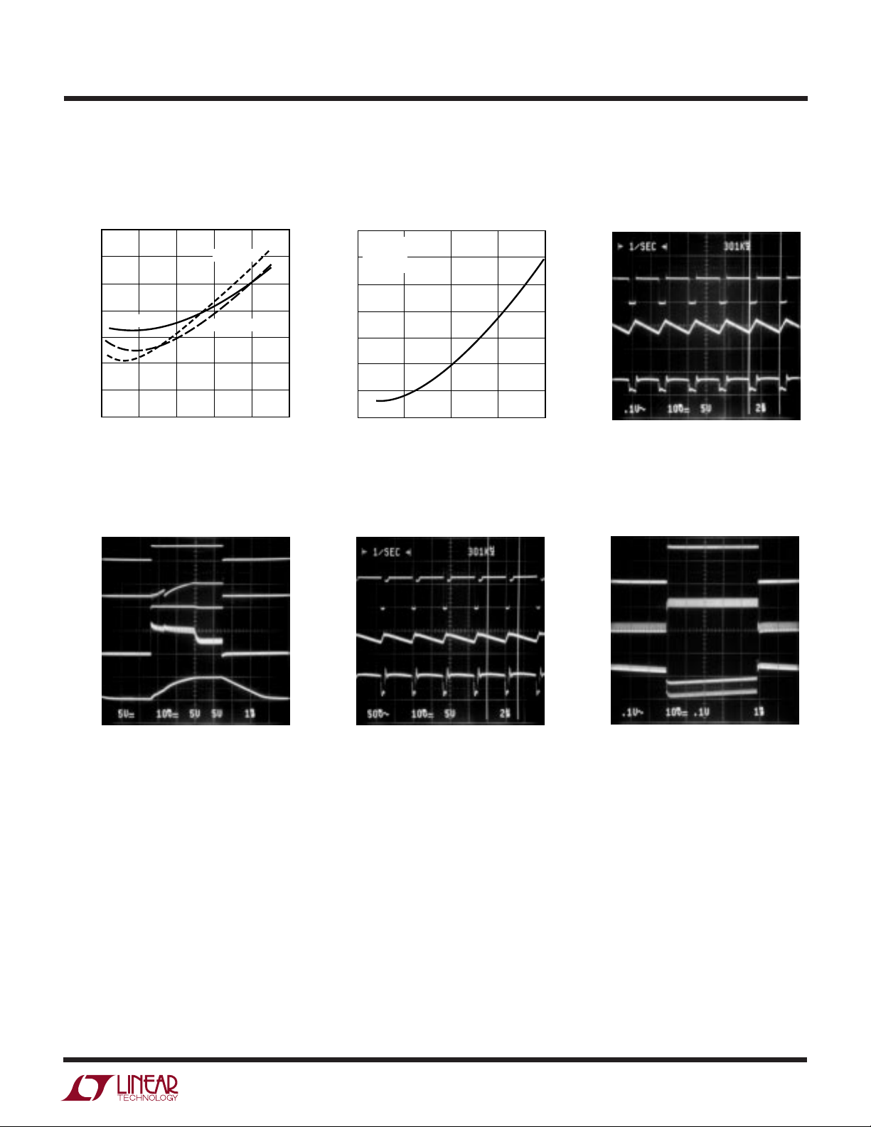
Start-Up to Shutdown Transient
Response*
V
S/S
5V/DIV
V
SW
5V/DIV
I
L
2A/DIV
V
O
5V/DIV
= 2.5V
V
IN
1ms/DIV
1.5
1306 • G13
1.65
RECTIFIER VOLTAGE (V)
1.60
1.55
0.5 1.0 2.0
0
RECTIFIER CURRENT (A)
Continuous-Conduction Mode
Switching Waveforms in
Stepdown Mode
V
SW
5V/DIV
I
L
0.5V/DIV
V
O
50mV/DIV
AC
VIN = 6V
V
= 5V
O
2µs/DIV
1.5
1306 • G14
0.1V/DIV
LOAD
CURRENT
0.5A/DIV
INDUCTOR
CURRENT
1A/DIV
OUTPUT
0.1V/DIV
V
O
AC
V
V
= 4.2V
IN
= 5V
O
2µs/DIV
Transient Response of the
Converter in Figure 1 with a
50mA to 800mA Load Step
DC
AC
VIN = 3.6V
V
= 5V
O
1ms/DIV
*Notice that the Input Start-Up Current is well Controlled and the
Output Voltage Falls to Zero in Shutdown.
5
Page 6

LT1306
UUU
PIN FUNCTIONS
VC (Pin 1): Compensation Pin for Error Amplifier. VC is
the output of the transconductance error amplifier. Loop
frequency compensation is done by connecting an RC
network from the VC pin to ground.
FB (Pin 2): Inverting Input of the Error Amplifier. Connect
the resistor divider tap here. Set output voltage according
to V
V
= 1.24V (1 + R1/R2).
OUT
(Pin 3): Output of the Switching Regulator and Emit-
OUT
ter of the Synchronous Rectifier. Connect appropriate
output capacitor from here to ground. V
must be kept
OUT
below 5.5V.
GND (Pin 4): Ground. Connect to local ground plane.
SW (Pin 5): Switch Pin. The collectors of the grounded
power switch and the synchronous rectifier. Keep the SW
trace as short as possible to minimize EMI.
W
BLOCK DIAGRA
V
IN
C
7
1
1.65V
–
A5
+
–
A3
V
+
B
1.24V
FB
V
+
A1
g
2
m
–
CAP (Pin 6): Power Supply to the Synchronous Rectifier
Driver. The bootstrap capacitor and the blocking diode
are tied to this pin. The CAP voltage switches between a
low level of VIN – VD to a high level determined by the V
SW
high level.
VIN (Pin 7): Supply or Battery Input Pin. Must be closely
bypassed to ground plane.
S/S (Pin 8): Shutdown and Synchronization Pin. Shut-
down is active low with a typical threshold of 0.9V. For
normal operation, the S/S pin is tied to VIN. To externally
synchronize the switching regulator, drive the S/S pin
with a pulse train.
I
> 0
IDLE
RECT
DCM
CAP
6
X3
X5
SW
5
CONTROL
UVLO
X4
6
I
RECT
OUT
3
–
A4
+
RAMP
COMPENSATION
300kHz OSC
8S/S
SHDN
SYNC
REF/BIAS
SHUTDOWN
DELAY
CLK
++
Σ
X1
S
Q
R
PWM CONTROL
Q2
RECTIFIER
X2
Q1
+
–
V
X4
CE2
+
A2
SENSE
AMP
–
4
GND
R
S
1306 F02
Figure 2. LT1306 Block Diagram
Page 7

OPERATIO
LT1306
U
The LT1306 is a fixed frequency current mode PWM
regulator with integrated power transistor Q1 and synchronous rectifier Q2.
In the Block Diagram, Figure 2, the PWM control circuit
is enclosed within the dashed line. It consists of the
current sense amplifier (A2), the oscillator, the compensating ramp generator, the PWM comparator (A4), the
logic (X1 and X2), the power transistor driver (X4) and
the main power switch (Q1). Notice that the clock (CLK)
“blanks” Q1 conduction. The internal oscillator frequency
is 300kHz.
The pulse width of the clock determines the maximum on
duty ratio of Q1. In the LT1306 this is set to 88%. Q1 turns
on at the trailing edge of the clock pulse. To prevent
subharmonic oscillation above 50% duty ratio, a compensating ramp (generated from the oscillator sawtooth)
is added to the sensed Q1 current. Q1 is turned off when
this sum exceeds the error amplifier A1 output, VC. Q1’s
absolute current limit is reached when VC’s upward
excursion is clamped internally at 1.28V.
The error amplifier output, VC, determines the peak switch
current required to regulate the output voltage. VC is a
measure of the output power. At heavy loads, the average
and the peak inductor currents are both high. VC moves to
the upper end of its operating range and the LT1306 operates in continuous conduction mode (CCM).
As load decreases, the average inductor current decreases. In CCM, the peak-to-peak inductor current ripple
to the first order depends only on the inductance, the
input and the output voltages. When the average inductor
current falls below 1/2 of the peak-to-peak inductor
current ripple, the converter enters discontinuous conduction mode (DCM). The switching frequency remains
constant except that the inductor current always returns
to zero within each switching cycle.
In both CCM and DCM, the output voltage is regulated
with negative feedback. A1 amplifies the error voltage
between the internally generated 1.24V reference and the
attenuated output voltage. The RC network from the V
pin to ground provides the loop compensation.
Further reduction in the load moves VC towards the lower
end of its operating range. Both the peak inductor current
C
and switch Q1’s on-time decrease. Hysteretic comparator
A3 determines if VC is too low for the LT1306 to operate
efficiently. As VC falls below the trip voltage VB, the output
of A3 goes high. All circuits except the error amplifier,
comparators A3 and A5, and the rectifier driver control X5,
are turned off. After the remaining energy stored in the
inductor is delivered to the output through the synchronous rectifier Q2, the LT1306 stops switching. In this idle
state, the LT1306 draws only 160µA from the input. With
switching stopped and the load being powered by the
output filter capacitor, the output voltage decreases. V
then starts to increase. Q1 does not start to switch until V
rises above the upper trip point of A3. The LT1306 again
delivers power to the output as a current mode PWM
converter except that the switch current limit is only about
250mA due to the low value of VC. If the load is still light,
the output voltage will rise and VC will fall, causing the
converter to idle again. Power delivery therefore occurs in
bursts. The on-off cycle frequency, or burst frequency,
depends on the operating conditions, the inductance and
the output filter capacitance. The output voltage ripple in
Burst Mode operation is usually higher than either CCM or
DCM operation. Burst Mode operation increases light load
efficiency because it delivers more energy to the output
during each clock cycle than is possible with DCM
operation’s extremely low peak switch current. This allows fewer switching cycles per unit time to maintain a
given output. Chip supply current therefore becomes a
small fraction of the total input current.
The synchronous rectifier is represented as NPN transistor, Q2, in the Block Diagram (Figure 2). A rectifier drive
circuit, X5, supplies variable base drive to Q2 and controls
the voltage across the rectifier. The supply voltage, V
for the driver is generated locally with the bootstrap circuit, D1 and C1 (Figure 1). When Q1 is on, the bootstrap
capacitor C1 is charged from the input to the voltage
VIN – V
the input through D1, C1 and Q1 to ground. After Q1 is
switched off, the node SW goes above VO by the rectifier
drop V
age is pushed up to VO + V
C1 supplies the base drive to Q2. The consumed charge is
replenished during the Q1 on interval.
– V
D1(ON)
. D1 becomes back-biased and the CAP volt-
CESAT2
. The charging current flows from
CESAT1
+ VIN – V
CESAT2
D1(ON)
– V
CAP
CESAT1
C
C
,
.
7
Page 8

LT1306
MODE
1306 F04
VO + 0.1VV
O
V
IN
BOOST
STEPDOWN
OPERATIO
U
In boost operation, X5 drives the rectifier Q2 into saturation. The voltage across the rectifier is V
CESAT
. As the
inductor current decreases, Q2’s base drive also decreases. X5 ceases supplying base current to Q2 when the
inductor current falls to zero.
If VIN > VO, Q2 will no longer be driven into saturation.
Instead the voltage across Q2 is allowed to increase so that
the inductor voltage reverses polarity as Q1 switches.
Since the inductor voltage is bipolar, volt-second balance
can be maintained regardless of the input voltage. The
LT1306 is therefore capable of operating as a step-down
regulator with the basic boost topology. Input
start-up current is also well controlled since the inductor
current cannot increase during Q1’s off-time with negative
inductor voltage.
The rectifier voltage drop depends on both the input and
the output voltages. Efficiency in the step-down mode is
less than that of a linear regulator. For sustained stepdown operation, the maximum output current will be
limited by the package thermal characteristics.
A hysteretic comparator in driver X5 controls the mode
of operation. DC transfer characteristics of the comparator are shown in Figure 3 and Figure 4.
A logic low at the S/S pin (Pin 8) initiates shutdown. First,
all circuit blocks in the LT1306 are switched off. The
synchronous rectifier Q2 and its driver are kept on to
allow stored inductive energy to flow to the output. As V
O
drops below VIN, the voltage across the rectifier Q2
increases so that the inductor voltage reverses. Inductor
current continues to fall to zero. Driver X5 then turns off
and the rectifier, Q2, becomes an open circuit. The
LT1306 dissipates only 9µA in shutdown.
The LT1306 is guaranteed to start with a minimum VIN of
1.8V. Comparator A5 senses the input voltage and generates an undervoltage lockout (UVLO) signal if VIN falls
below this minimum. In UVLO, VC is pulled low and Q1
stops switching. The LT1306 draws 160µA from the
input.
MODE
BOOST
STEPDOWN
0
Figure 3. DC Transfer Characteristics of the Mode Control
Comparator Plotted with VO as an Independent Variable.
VIN is Considered Fixed.
VIN – 0.1V V
IN
1306 F03
V
O
Figure 4. DC Transfer Characteristics of the Mode Control
Comparator Plotted with VIN as an Independent Variable.
VO is Considered Fixed.
8
Page 9

LT1306
U
WUU
APPLICATIONS INFORMATION
Output Voltage Setting
The output voltage of the LT1306 is set with a resistive
divider, R1 and R2 (Figure 1 and Figure 5), from the output
to ground. The divider tap is tied to the FB pin. Current
through R2 should be significantly higher than the FB pin
input bias current (≤25nA). With R2 = 249k, the input bias
current of the error amplifier is 0.5% of the current in R1.
V
O
R1
V
= 1.24V 1 +
O
FB PIN
R1 = R2
R2
Figure 5. Feedback Resistive Divider
Synchronization and Shutdown
The S/S pin (Pin 8) can be used to synchronize the
oscillator or disconnect the load from the input. The S/S
pin is tied to the input (VIN > 1.8V) for normal operation.
The oscillator in the LT1306 can be externally synchronized by driving the S/S pin with a pulse train (See the
graph “Maximum Allowable Rise Time of Synchronizing
Pulse” in the Typical Performance Characteristics). The
synchronization is positive edge triggered. The recommended frequency of the external clock ranges from
425kHz to 500kHz. If synchronization results in switching
jitter, reducing the rising edge dv/dt of the external clock
pulse usually cures the problem.
R1
()
R2
V
O
– 1
()
1.24
1306 F05
The inductor should be able to handle the full load peak
inductor current without saturation. The peak inductor
current can be as high as 2A. This places a lower limit on
the core size of the inductor. Powder iron cores have
unacceptable core losses and are not suitable for high
efficiency applications. Most ferrite core materials have
manageable core losses and are recommended. Inductor
DC winding resistance (DCR) also needs to be considered
for efficiency. Usually there are trade-offs between core
loss, DCR, saturation current, cost and size.
For EMI sensitive applications, one may want to use
magnetically shielded or toroidal inductors to contain field
radiation. Table 1 lists a number of inductors suitable for
LT1306 applications.
Table 1. Inductors Suitable for Use with the LT1306
PART VALUE MAX DCR CORE HEIGHT
VENDOR NO. (µH) (Ω) TYPE (mm)
BH Electronics 511-0033 5.0 0.023 Toroid 4.8
Coilcraft DO3308-103 10 0.09 Open 3.0
DO3316-472 4.7 0.018 Open 5.2
DO3316-103 10 0.029 Open 5.2
DO3316-153 15 0.046 Open 5.2
Coiltronics CTX5-2 5 0.021 Toroid 6.0
CTX10-2 10 0.032 Toroid 6.0
Murata LQN6C4R7 4.7 0.034 Open 5.0
Sumida CDRH73-100 10 0.072 Magnetic 3.4
Shielding
CD43-4R7 4.7 0.109 Open 3.2
Capacitors
Shutdown will be activated if the S/S pin voltage stays
below the shutdown threshold (0.45V) for more than
50µs. This shutdown delay is reset whenever the S/S pin
goes above the shutdown threshold.
Inductor
The value of the energy storage inductor L1 (Figure 1) is
usually selected so that the peak-to-peak ripple current is
less than 40% of the average inductor current. For 1- or
2-cell alkaline or single Li-Ion to 5V applications, 10µH to
20µH is recommended for the LT1306 running at 300kHz.
A 5µH to 10µH inductor can be used if the LT1306 is
externally synchronized at 500kHz.
The output filter capacitor is usually chosen based on its
equivalent series resistance (ESR) and the acceptable
change in output voltage as a result of load transients. The
output voltage ripple at the switching frequency can be
estimated by considering the peak inductor current and
the capacitor ESR.
IV
OO
II
≈≈
PEAK IN
output ripple ≅ (ESR)(I
()( )
V
IN
PEAK
ESR I V
()()()
OO
) =
V
IN
9
Page 10

LT1306
U
WUU
APPLICATIONS INFORMATION
Since a boost converter produces high output current
ripple, one also needs to consider the maximum ripple
current rating of the output capacitor. Capacitor reliability
will be affected if the ripple current exceeds the maximum
allowable ratings. This maximum rating is usually
specified as the RMS ripple current. In the LT1306 the
RMS output capacitor ripple current is:
–
VV
OIN
I
O
V
IN
For 2-cell to 5V applications, 220µF low ESR solid tanta-
lum capacitors (AVX TPS series or Sprague 593D series)
work well. To reduce output voltage ripple due to heavy
load transients or Burst Mode operation, higher capacitance may be used. For through-hole applications, Sanyo
OS-CON capacitors are also good choices.
In a boost regulator, the input capacitor ripple current is
much lower. Maximum ripple current rating and input
voltage ripples are not usually of concern. A 22µF tantalum
capacitor soldered near the input pin is generally an
adequate bypass.
Bootstrap Supply
Diode D1 and capacitor C1 generate a pulsating supply
voltage, V
drive circuit runs off this supply. During rectifier on-time,
the rectifier base current drains C1. Q2 base current and
the maximum allowable V
size of C1. A 1µF capacitor is sufficient to keep V
below 0.3V. For a 2-cell input (VIN > 1.8V) over an extended
temperature range, a BAT54 Schottky diode may be used
for D1. The use of a Schottky diode increases the bootstrap
voltage and the operating headroom for the rectifier driver,
X5. Diodes like a 1N4148 or 1N914 work well for 2-cell
inputs over the 0°C to 70°C commercial temperature
range.
, which is higher than the output. The rectifier
CAP
ripple voltage determine the
CAP
CAP
ripple
switch and can cause the current limit comparator to trip
erratically. For boost applications where VIN is a few tenths
of a volt below VO, a 1µF or 2.2µF tantalum capacitor (such
as AVX TAJ series) can be used for C1. The ESR of the
tantalum capacitor limits the charging current. A low value
resistor (2Ω to 5Ω) can also be added in series with C1 for
further limiting the charging current although this tends to
lower the converter efficiency slightly.
Frequency Compensation
Current mode switching regulators have two feedback
loops. The inner current feedback loop controls the
inductor current in response to the outer loop. The outer
or overall feedback loop tightly regulates the output
voltage. The high frequency gain asymptote of the inner
current loop rolls off at –20dB/decade and crosses the
unity gain axis at a frequency ωc between 1/6 to 2/3 of the
switching frequency. The current loop is stable and is
wideband compared to the overall voltage feedback loop.
The low frequency current loop gain is not high (usually
between unity and 10) but it increases the low frequency
impedance of the inductor as seen by the output filter
capacitor. (In a boost regulator, the inductor is connected to the output during the switch off-time.) Current
mode control introduces an effective series resistance
(>>DCR) to the inductor that damps the LC tank response. The complex high-Q poles of the LC filter are now
separated, resulting in a dominant pole determined by
the filter capacitance and the load resistance and a
second high frequency pole.
For a boost regulator the control to output transfer function can be shown to have a dominant pole at the load
corner frequency
ω
=
P
R
L
2
1
C
()
O
The charge drawn from C1 during the rectifier on-time has
to be replenished during the switch on-interval. As duty
cycle decreases, the amplitude of the C1 charging current
can increase dramatically especially when delivering high
power to the load. This charging current flows through the
10
and a moving right-half plane (RHP) zero with a minimum
value of
RD
12–
()
=
Z
L MAX
L
ω
Page 11

LT1306
C
R
P
Z
=
1
33ω
U
WUU
APPLICATIONS INFORMATION
where
R Maximum Load
==
L
D MaximumConverter DutyCycle
=
MAX
VV
–.
O IN MIN
=
There is also a second pole at the current loop crossover
frequency ωC (Figure 6). ωZ is much lower in frequency
than ωC. The loop is compensated by adjusting the midband
gain with resistor R3 (Figure 7) so that the overall loop gain
crosses 0dB before the minimum frequency RHP zero
(i.e., corresponding to the highest duty ratio). The value of
R3 can be estimated with the fromula:
R
Due to the low transconductance of the error amplifier, the
gain setting resistor R3 is AC-coupled with capacitor CZ.
This prevents R3 from inducing an offset to the input of the
error amplifier. It also creates a pole at DC and a low
frequency zero.
The amplitude response of the error amplifier with the
compensation network shown is:
V
O
390 1=(– )
3
+
.
01
05
L
()
+
VDCR
O MAX O L
Output Voltage
MaximumDCLoad Current
The low frequency zero 1/R3CZ of the compensation
network is placed at ωP/2.
C
The capacitor CP ensures adequate gain margin beyond
the RHP zero. The high frequency pole 1/R3CP of the
amplifier frequency response is placed beyond ωZ.
Higher output filter capacitance rolls off the gain response
from a lower corner frequency so higher midband gain is
required in the compensation network to make the overall
loop gain cross 0dB just below ωZ.
Layout Consideration
To minimize EMI and high frequency resonances, it is
essential to keep the SW and the CAP trace leads as short
as possible. The input and the output bypass capacitors
CIN and C
soldered to the ground plane. A ground plane under the
switching regulator is highly recommended. Figure 8
shows a suggested component placement and PC board
layout.
2
=
Z
R
3ω
P
should be placed close to the IC package and
OUT
••
SR C
13
ˆ
V
C
ˆ
V
O
CC
ZP
=
>>
g
m
R
2
RR
12
+
+
()
•••
SC SR C
+
13
ZP
()
[]
Z
11
Page 12

LT1306
U
WUU
APPLICATIONS INFORMATION
GAIN
(dB)
MIDBAND GAIN =
AMOUNT OF
MIDBAND GAIN
NEEDED
ω
(R3)(C
1
)
Z
P
1
R
(CO)
L
()
2
LOOP GAIN
CROSSOVER
FREQUENCY ≈
1
ω
Z
3
AMPLITUDE RESPONSE OF
TRANSFER FUNCTION BEFORE
0
(gm)(R3)(R2)
R1 + R2
ω
Z
CONTROL-TO-OUTPUT
COMPENSATION
ˆ
V
C
ˆ
V
O
RHP ZERO =
ω
C
OVERALL LOOP GAIN
AFTER COMPENSTION
(1 – D
R
L
MAX
L
CURRENT LOOP
CROSSOVER
FREQUENCY
ˆ
V
O
ˆ
V
C
2
)
AMPLITUDE RESPONSE
OF THE ERROR AMPLIFIER
ω
1306 F06
Figure 6. Gain Asymptotes of the Control-to-Output
V
IN
L
PWM CONTROL
LOGIC
LT1306
V
C
R3
C
Z
SW
C
P
ˆ
V
O
and Error Amplifier
ˆ
V
C
Q2
Q1
RECTIFIER
–
g
m
+
1.24V
GND
R1
FB
R2 R
ˆ
V
C
Transfer Function
ˆ
V
O
I
C
L
O
1306 F07
V
O
O
12
Figure 7. Current Mode Boost Converter Overall-Loop Compensation
Page 13

LT1306
U
WUU
APPLICATIONS INFORMATION
GROUND PLANE
R2
+
V
OUT
C
VIAS
O1
C
Z
R3
C
P
V
C
1
R1
2
3
4
LT1306
C
IN2
S/S
V
IN
8
7
6
5
+
C1
D1
+
C
C
O2
GND
IN1
L1
Figure 8. Recommended Component Placement for LT1306.
Notice That the Input and the Output Capacitors Are Grounded
at the Same Point. A Ground Plane Under the DC/DC Converter
Is Highly Recommended. Use Multiple Vias to Tie Pin 4 Copper
to the Ground Plane
1306 F08
13
Page 14

LT1306
TYPICAL APPLICATIO S
2V
TO 3V
C
IN1
0.1µF
CERAMIC
U
+
2-Cell NiMH to 3.3V Output
D1
C1
L1
1µF
4.7µH
2V/500kHz
C
IN2
22µF
5.6nF
V
R3
95k
C
Z
SW
IN
LT1306
V
C
C
P
39pF
CAP
OUTS/S
GND
+
3.3V
R1
412k
FB
R2
249k
1306 F09
1A
+
C
O
220µF
C
: AVX TAJC226M010
IN1
: AVX TPSE227M010R0100
C
O1
C1: AVX TAJA105K020
D1: CMDSH-3
L1: LQN6C4R7
90
VO = 3.3V
L1 = 4.7µH
85
80
75
EFFICIENCY (%)
70
65
60
1
Efficiency
VIN = 3V
VIN = 2.5V
VIN = 1.8V
10 100 1000 2000
LOAD CURRENT (mA)
1306 F09a
14
Page 15

PACKAGE DESCRIPTION
U
Dimensions in inches (millimeters) unless otherwise noted.
S8 Package
8-Lead Plastic Small Outline (Narrow 0.150)
(LTC DWG # 05-08-1610)
0.189 – 0.197*
(4.801 – 5.004)
7
8
5
6
LT1306
0.228 – 0.244
(5.791 – 6.197)
0.010 – 0.020
(0.254 – 0.508)
0.008 – 0.010
(0.203 – 0.254)
*
DIMENSION DOES NOT INCLUDE MOLD FLASH. MOLD FLASH
SHALL NOT EXCEED 0.006" (0.152mm) PER SIDE
**
DIMENSION DOES NOT INCLUDE INTERLEAD FLASH. INTERLEAD
FLASH SHALL NOT EXCEED 0.010" (0.254mm) PER SIDE
×
°
45
0.016 – 0.050
(0.406 – 1.270)
(1.346 – 1.752)
0°– 8° TYP
0.053 – 0.069
0.014 – 0.019
(0.355 – 0.483)
TYP
0.150 – 0.157**
(3.810 – 3.988)
1
3
2
4
0.004 – 0.010
(0.101 – 0.254)
0.050
(1.270)
BSC
SO8 1298
Information furnished by Linear Technology Corporation is believed to be accurate and reliable.
However, no responsibility is assumed for its use. Linear Technology Corporation makes no representation that the interconnection of its circuits as described herein will not infringe on existing patent rights.
15
Page 16

LT1306
U
TYPICAL APPLICATIO S
4-Cell NiMH to 5V Output Efficiency
3.6V
TO 6.5V
D1
C1
L1
1µF
10µH
V
IN
+
C
22µF
C
IN1
IN2
0.1µF
CERAMIC
15nF
LT1306
V
C
R3
75k
C
Z
SW
C
P
22pF
CAP
OUTS/S
GND
+
5V
R1
768k
FB
R2
249k
+
C
O1
220µF
1306 F09
1A
C
O2
1µF
CERAMIC
: AVX TAJC226M010
C
IN1
: AVX TPSE227M010R0100
C
O1
C1: AVX TAJA105K020
D1: MMBD914LT1
L1: CTX10-3
90
VO = 5V
L1 = 10µH
85
80
75
EFFICIENCY (%)
70
65
60
1
VIN = 4.8V
VIN = 3.6V
VIN = 6V
10 100 1000 2000
LOAD CURRENT (mA)
1306 F10a
Transient Response with Step Input (4V to 6V)
V
IN
5V/DIV
V
SW
5V/DIV
I
L
500mA/DIV
V
O
0.1V/DIV
AC
0.5ms/DIV
RELATED PARTS
PART NUMBER DESCRIPTION COMMENTS
LT1302 High Output Current Micropower DC/DC Converter 5V/600mA from 2V, 2A Internal Switch, 200µA I
LT1304 2-Cell Micropower DC/DC Converter 5V/200mA, Low-Battery Detector Active in Shutdown
LT1307/LT1307B Single Cell, Micropower, 600kHz PWM DC/DC Converters 3.3V at 75mA from One Cell, MSOP Package
LT1308A/LT1308B High Output Current Micropower DC/DC Converter 5V at 1A from Single Li-Ion Cell
LT1316 Burst Mode Operation DC/DC with Programmable Current Limit 1.5V Minimum, Precise Control of Peak Current Limit
LT1317/LT1317B Micropower, 600kHz PWM DC/DC Converters 100µA IQ, Operate with VIN as Low as 1.5V
LT1610 Single-Cell Micropower DC/DC Converter 3V at 30mA from 1V, 1.7MHz Fixed Frequency
LT1613 1.4MHz Switching Regulator in 5-Lead SOT-23 5V at 200mA from 4.4V Input, Tiny SOT-23 package
LT1615 Micropower Step-Up DC/DC in 5-Lead SOT-23 20µA IQ, 36V/350mA Internal Switch, VIN as Low as 1.2V
LTC1624 High Efficiency N-channel Switching Regulator Controller V
= 1.19V to 30V in Stepdown; VIN = 3.5V to 36V
OUT
SO-8 Package
LT1949 600kHz, 1A Switch PWM DC/DC Converter 1.1A, 0.5Ω/30V Internal Switch, VIN as Low as 1.5V
1306f LT/TP 0400 4K • PRINTED IN USA
LINEAR TECHNOLOGY CORPORATION 1999
16
Linear Technology Corporation
1630 McCarthy Blvd., Milpitas, CA 95035-7417
(408) 432-1900 ● FAX: (408) 434-0507
●
www.linear-tech.com
Q
 Loading...