

Page 1
LT1305
Micropower High Power
DC/DC Converter with
Low-Battery Detector
EATU
F
■
5V at 400mA from 2V Input
■
Supply Voltage As Low As 1.8V
■
120µA Quiescent Current
■
Low-Battery Detector
■
Low V
■
Uses Inexpensive Surface Mount Inductors
■
8-Lead SO Package
PPLICATI
A
■
2-Cell and 3-Cell to 5V Conversion
■
EL Panel Drivers
■
Portable Instruments
S
RE
Switch: 310mV at 2A Typ
CESAT
U
O
S
A
PPLICATITYPICAL
O
U
DUESCRIPTIO
The LT®1305 is a micropower step-up DC/DC converter
that uses Burst ModeTM operation. Similar to the LT1303,
the LT1305 features a 2A internal low-loss switch and can
deliver up to four times the output power of the LT1303.
Quiescent current is only 120µA and the Shutdown pin
further reduces current to 10µA. A low-battery detector
provides an open-collector output that goes low when the
input voltage drops below a preset level. The LT1305 is
available in an 8-pin SO, easing board space requirements.
, LTC and LT are registered trademarks of Linear Technology Corporation.
Burst Mode is a trademark of Linear Technology Corporation
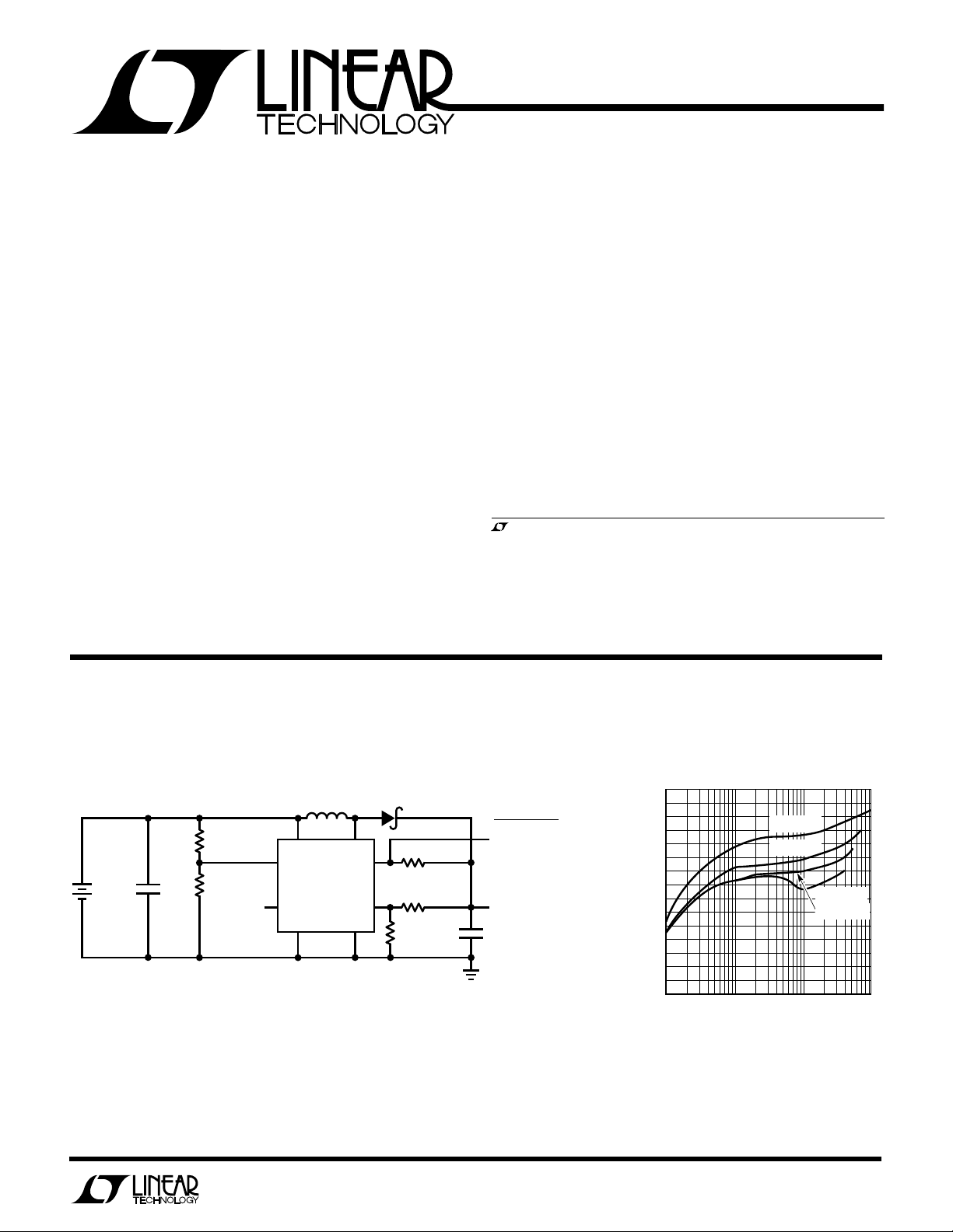
2-Cell and 3-Cell to 5V/400mA DC/DC Converter
with Low-Battery Detect
316k
1%
2 TO 3
CELLS
C1, C2: AVX TPSE227010R0100
D1: MOTOROLA MBRS130LT3
L1: COILCRAFT D03316-103
+
C1
220µF
412k
1%
SHUTDOWN
L1
10µH
V
IN
LBI
LT1305
SHDN
GND PGND
SW
LBO
Efficiency
D1
LOW BATTERY
100k
301k
100k
1%
1%
C2
220µF
FB
GOES LOW AT
= 2.2V
V
BAT
V
OUT
5V
400mA
+
LT1305 • TA03
90
80
EFFICIENCY (%)
70
60
1
VIN = 4.00V
VIN = 3.00V
= 2.00V
V
IN
VIN = 2.50V
10 100 1000
LOAD CURRENT (mA)
LT1305 • TA02
1
Page 2
LT1305
WU
U
PACKAGE
/
O
RDER I FOR ATIO
W
O
A
LUTEXI T
S
VIN Voltage .............................................................. 10V
SW1 Voltage ............................................................ 25V
FB Voltage ............................................................... 10V
Shutdown Voltage ................................................... 10V
LBO Voltage............................................................. 10V
LBI Voltage .............................................................. 10V
Maximum Power Dissipation ............................. 500mW
Operating Temperature Range ..................... 0°C to 70°C
Storage Temperature Range ................. –65°C to 150°C
A
WUW
ARB
U
G
I
S
GND
LBO
SHDN
1
2
3
FB
4
T
JMAX
TOP VIEW
S8 PACKAGE
8-LEAD PLASTIC SO
= 100°C, θJA = 80°C/ W
ORDER PART
NUMBER
PGND
8
SW
7
V
6
IN
LBI
5
LT1305CS8
S8 PART MARKING
1305
Lead Temperature (Soldering, 10 sec)..................300°C
Consult factory for Industrial and Military grade parts.
LECTRICAL C CHARA TERIST
E
SYMBOL PARAMETER CONDITIONS MIN TYP MAX UNITS
I
Q
VINInput Voltage Range 1.8 1.55 V
DC Maximum Duty Cycle ● 75 86 95 %
t
ON
V
CESAT
V
SHDNH
V
SHDNL
I
SHDN
Quiescent Current V
Feedback Voltage ● 1.22 1.24 1.26 V
Comparator Hysteresis ● 6 12.5 mV
Feedback Pin Bias Current VFB = 1V ● 720 nA
Oscillator Frequency Current Limit Not Asserted 120 155 185 kHz
Oscillator TC 0.2 %/°C
Switch On Time Current Limit Not Asserted 5.6 µs
Output Line Regulation 1.8V < VIN < 6V ● 0.06 0.15 %/V
Switch Saturation Voltage ISW = 1A ● 140 280 mV
Switch Leakage Current VSW = 5V, Switch Off ● 0.1 10 µA
Peak Switch Current VIN = 2V 1.35 2 2.35 A
LBI Trip Voltage (Note 2) ● 1.21 1.24 1.27 V
LBI Input Bias Current V
LBO Output Low I
LBO Leakage Current V
Shutdown Pin High ● 1.8 V
Shutdown Pin Low 0.5 V
Shutdown Pin Bias Current V
ICS
TA = 25°C, VIN = 2.0V, unless otherwise noted.
= 0.5V, VFB = 2V ● 120 200 µA
SHDN
V
= 1.8V ● 715 µA
SHDN
● 2.0 V
● 1.20 2.50 A
VIN = 5V 1.15 2.15 A
= 1V ● 720 nA
LBI
= 100µA ● 0.11 0.4 V
LOAD
= 1.3V, V
LBI
= 5V ● 8.0 20 µA
SHDN
= 2V ● 3.0 µA
V
SHDN
= 0V ● 0.1 1 µA
V
SHDN
= 5V ● 0.1 5 µA
LBO
The ● denotes specifications which apply over the 0°C to 70°C operating
temperature range.
Note 1: Hysteresis specified is DC. Output ripple may be higher if output
capacitance is insufficient or capacitor ESR is excessive.
2
Note 2: Low-battery detector comparator is inoperative when device is in
shutdown.
Page 3
W
TEMPERATURE (˚C)
–50
1.8
2.0
2.2
25 75
LT1305 • G06
1.6
1.4
–25 0
50 100
1.2
1.0
PEAK SWITCH CURRENT (A)
2.4
TEMPERATURE (°C)
–50
1.200
FEEDBACK VOLTAGE (V)
1.210
1.215
1.220
1.225
1.230
1.235
–25
0
25 50
LT1305 • G09
75
1.240
1.245
1.250
1.205
100
U
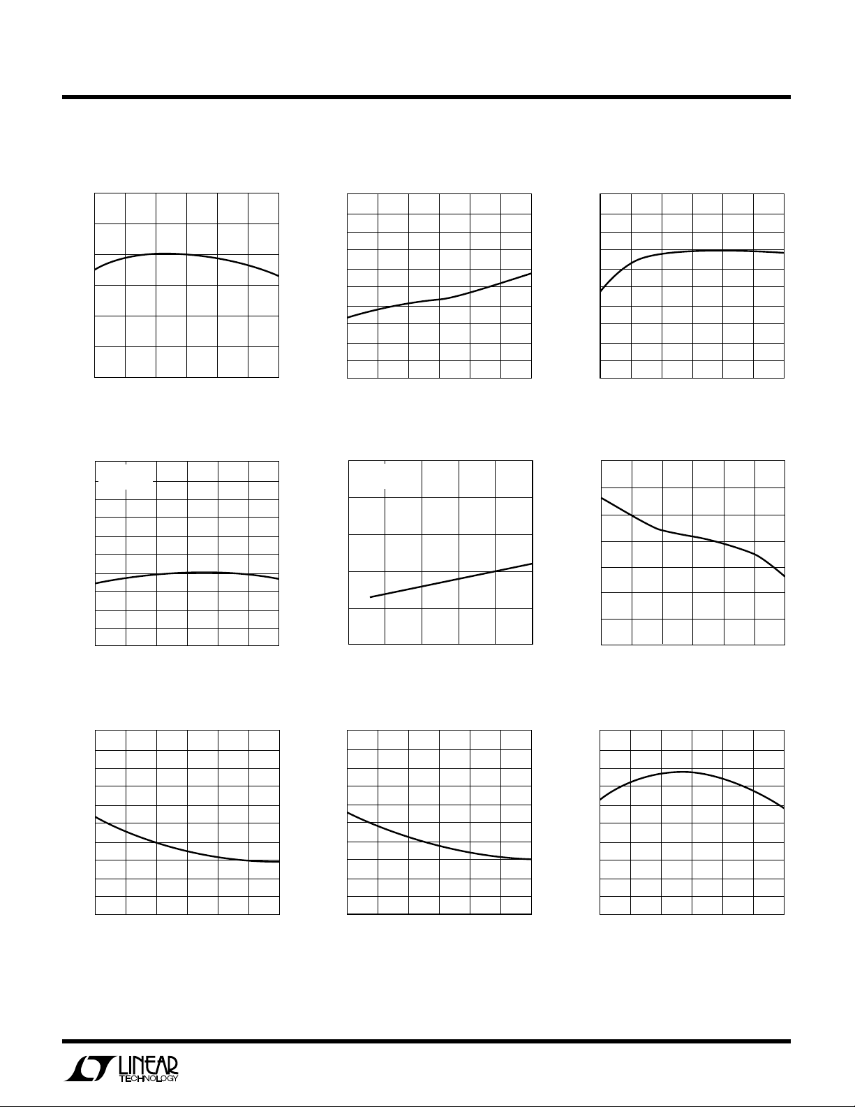
TYPICAL PERFORMANCE CHARACTERISTICS
LT1305
Switch On Time
8
7
6
5
ON TIME (µs)
4
3
2
–50
–25
02550
TEMPERATURE (°C)
75 100
LT1305 • G01
Oscillator Frequency
200
190
180
170
160
150
140
FREQUENCY (kHz)
130
120
110
100
–50
–25
Quiescent Current Quiescent Current
QUIESCENT CURRENT (µA)
500
400
300
200
100
0
TA = 25°C
SWITCH OFF
0
2
200
190
180
170
160
150
140
130
QUIESCENT CURRENT (µA)
120
110
100
SWITCH OFF
V
IN
–50
= 2V
–25
TEMPERATURE (°C)
0
25 50
75
LT1305 • G04
100
25 50
0
TEMPERATURE (°C)
6
4
INPUT VOLTAGE (V)
75
LT1305 • G02
8
LT1305 • G05
100
10
Maximum Duty Cycle
100
95
90
85
80
75
70
DUTY CYCLE (%)
65
60
55
50
–50
–25
TEMPERATURE (°C)
Current Limit
0
25 50
75
LT1305 • G03
100
LBI Pin Bias Current FB Pin Bias Current
20
18
16
14
12
10
8
BIAS CURRENT (nA)
6
4
2
0
–50
–25
25 50
0
TEMPERATURE (°C)
75
LT1305 • G07
100
20
18
16
14
12
10
8
BIAS CURRENT (nA)
6
4
2
0
–50
–25
25 50
0
TEMPERATURE (°C)
75
LT1305 • G08
FB Voltage
100
3
Page 4

LT1305
TEMPERATURE (°C)
–50
0
SWITCH SATURATION VOLTAGE (mV)
50
100
150
200
300
–25
02550
LT1305 • G13
75 100
250
ISW = 1A
W
U
TYPICAL PERFORMANCE CHARACTERISTICS
Low-Battery Detect Trip Point
1.250
1.245
1.240
1.235
1.230
1.225
1.220
LBI VOLTAGE (V)
1.215
1.210
1.205
1.200
–50
–25
25 50
0
TEMPERATURE (°C)
U
100
75
LT1305 • G10
UU
Switch Saturation Voltage
400
TA = 25°C
350
300
250
200
150
100
50
SWITCH SATURATION VOLTAGE (mV)
0
0.4
0.2
0
0.6
SWITCH CURRENT (A)
PI FU CTIO S
GND (Pin 1): Signal Ground. Tie to PGND under the
package.
LBO (Pin 2): Open-Collector Output of Comparator C3.
Can sink 100µA. High impedance when device is in shut-
down.
Switch Saturation Voltage
1.2
1.0
1.4
1.6
2.0
0.8
1.8
LT1305 • F12
LBI (Pin 5): Low-Battery Comparator Input. When voltage
on this pin is below 1.24V, LBO is low.
VIN (Pin 6): Supply Pin. Must be bypassed with a large
value capacitor to gound. Keep bypass within 0.2" of the
device.
SHDN (Pin 3): Shutdown. Pull high to shut down the
LT1305. Ground for normal operation.
FB (Pin 4): Feedback Input. Connects to main comparator
C1 input.
4
SW (Pin 7): Switch Pin. Connect inductor and diode here.
Keep layout short and direct to minimize radio frequency
interference.
PGND (Pin 8): Power Ground. Tie to signal ground (pin 1)
under the package. Bypass capacitor from VIN should be
tied directly to PGND within 0.2" of the device.
Page 5

BLOCK DIAGRAM
LT1305
W
SW
Q1
160×
D1
++
+
–
L1
36mV
R1
3Ω
Q2
1×
V
IN
C5 C4
R1
FB
4
R2
V
IN
6 7
CURRENT
COMPARATOR
C2
HYSTERETIC
COMPARATOR
OFF
–
A3
DRIVER
REFERENCE
1.24V
C1
OSCILLATOR
+
–
C3
+
LBOLBIGND
1
25
SHUTDOWN
3
PGND
8
LT1305 • F01
Figure 1. LT1305 Block Diagram
U
OPERATION
Operation of the LT1305 is best understood by referring to
the Block Diagram in Figure 1. When C1’s negative input,
related to the output voltage by the appropriate resistordivider ratio, is higher than the 1.24V reference voltage,
C1’s output is low. C2, A3 and the oscillator are turned off,
drawing no current. Only the reference and C1 consume
current, typically 120µA. When C1’s negative input drops
below 1.24V and overcomes C1’s 6mV hysteresis, C1’s
output goes high, enabling the oscillator, current comparator C2 and driver A3. Quiescent current increases to 2mA
as the device goes into active switching mode. Q1 then
turns on in controlled saturation for nominally 6µ s or until
current comparator C2 trips, whichever comes first. The
switch then turns off for approximately 1.5µ s, then turns on
again. The LT1305’s switching causes current to alternately build up in L1 and dump into output capacitor C4 via
D1, increasing the output voltage. When the output is high
enough to cause C1’s output to go high, switching action
ceases. Capacitor C4 is left to supply current to the load
until V
decreases enough to force C1’s output high, and
OUT
the entire cycle repeats. Figure 2 details relevant waveforms. C1’s cycling causes low-to-mid-frequency ripple
voltage on the output. Ripple can be reduced by making the
output capacitor large. The 220µ F unit specified results in
ripple of 50mV to 100mV on the 5V output. Paralleling two
capacitors will decrease ripple by approximately 50%.
V
OUT
100mV/DIV
AC COUPLED
V
SW
5V/DIV
I
L
1A/DIV
50µs/DIV
Figure 2. Burst Mode Operation
LT1305 • F02
5
Page 6

LT1305
U
OPERATION
If switch current reaches 2A, causing C2 to trip, switch on
time is reduced and off time increases slightly. This allows
continuous operation during bursts. C2 monitors the
voltage across 3Ω resistor R1 which is directly related to
the switch current. Q2’s collector current is set by the
emitter-area ratio to 0.6% of Q1’s collector current. When
R1’s voltage drop exceeds 36mV, corresponding to 2A
switch current, C2’s output goes high, truncating the on
time portion of the oscillator cycle and increasing off time
to about 2µs. Response time of C2, which determines
minimum on time, is approximately 300ns.
Low-Battery Detector
The low-battery detector is enabled when SHDN is low and
disabled when SHDN is high. The comparator has no
hysteresis built in, but hysteresis can be added by
connecting a high-value resistor from LBI to LBO as
shown in Figure 3. The internal reference can be accessed
via the comparator as shown in Figure 4.
V
BAT
R1
R2
49.9k
1%
R1 = (V
HYSTERESIS ≈ 30mV
Figure 3. R3 Adds Hysteresis to Low-Battery Detector
–1.24V) (43.5k)
TRIP
1.24V
LBI
V
–
+
IN
LT1305
R3
2M
LBO
5V
R4
47k
LT1305 • F03
Inductor Selection
Inductors used with the LT1305 must fulfill two requirements. First, the inductor must be able to handle current
of 2A to 2.5A without runaway saturation. Rod or drum
core units usually saturate gradually and it is acceptable to
exceed manufacturer’s published saturation current by
20% or so. Second, the unit must have low DCR, under
0.05Ω so that copper loss is kept low and excess heating
is avoided. Inductance value is not critical. Generally, for
low voltage inputs below 3V a 10µH inductor is recom-
mended (such as Coilcraft DO3316-103). For inputs above
4V to 5V use a 22µ H unit (such as Coilcraft DO3316-223).
Switching frequency can reach up to 300kHz so the core
material should be able to operate at high frequency
without excessive core loss. Ferrite or molypermalloy
cores are a better choice than powdered iron. If EMI is a
concern, a toroidal inductor is suggested, such as
Coiltronics CTX20-4.
Capacitor Selection
Output and input capacitors should have low ESR for best
performance. Inexpensive aluminum electrolytics sometimes have ESR above 1Ω, even for relatively large values
such as 100µF, 16V units. Since the LT1305 has a 2A
current limit, 2V of ripple voltage would result with such a
capacitor at the output. Keep ESR below 0.05Ω to 0.1Ω for
reasonable ripple voltage. Tantalum capacitors such as
AVX TPS series or Sprague 593D have low ESR and are
surface mount components. For lowest ESR, use Sanyo
OS-CON units (OS-CON is also available from Vishay).
These capacitors have superior ESR, small size and perform well at cold temperatures.
6
100k
2N3906
V
REF
OUTPUT
= 1.24V 1 +
V
REF
VIN ≥ V
REF
R1 + R2 ≈ 33k
Figure 4. Accessing Internal Reference
R2
+
2.2µF
R2
()
R1
+ 200mV
V
IN
LBO
LT1305
LBI
GND
R1
LT1305 • F04
Diode Selection
A 2A Schottky diode such as Motorola MBRS130LT3 is a
good choice for the rectifier diode. A 1N5821 or
MBRS130T3 are suitable as well. Do not use “general
purpose” diodes such as 1N4001. They are much too slow
for use in switching regulator applications.
Page 7

U
V
IN
3.5V to 6.5V
SHDN
100k
4 CELLS
100µF
150µF**
22µH*
100µF**
SHUTDOWN
LT1305
GND PGND
FB
SW
LT1305 • TA05
L1*
22µH
309k
+
COILCRAFT DO3316-223 OR
SUMIDA CD105-220
SANYO OS-CON
*
**
5V
400mA
+
MBRS130LT3
+
TYPICAL APPLICATIONS N
LT1305
4-Cell-to-5V ConverterSetting Output Voltage
SW
1N5817
V
OUT
R2
+
FB
220µF
R1
LT1305 • TA03
V
IN
+
100µF
V
= 1.24V 1 +
OUT
L1
V
IN
LT1305
GND PGND
R2
()
R1
5V Step-Up Converter with Reference Output
MBRS130LT3
SW
FB
309k
100k
5V
400mA
+
220µF
V
REF
OUTPUT
1.24V
1.8V TO 4.5V
INPUT
2N3906
+
2.2µF
33k
100k
+
100µF
10µH*
V
IN
LBO
LT1305
LBI
GND PGND
1.5V TO 8V
V
IN
100Hz TO 1000Hz
+
47µF
SQUARE WAVE
DRIVE
*COILCRAFT DO3316-103
LT1305 • TA06
EL Panel Driver
T1**
1:15
•
4, 5 6
•
SW
FBSHDN
OUT
83V
10
R1†
25k
1N5818
RMS
3.3M
3.3M
51k
TO 115V
10Ω
1, 2
V
††
0.1µF
CERAMIC
SHUTDOWN
Information furnished by Linear Technology Corporation is believed to be accurate and reliable.
However, no responsibility is assumed for its use. Linear Technology Corporation makes no representation that the interconnection of its circuits as described herein will not infringe on existing patent rights.
IN
LT1305
GND PGND
ADD C1 FOR OPEN-PANEL PROTECTION
*
DALE LPE5047-A132 1:15 TURNS RATIO
**
10µH PRIMARY INDUCTANCE (605) 666-9301
†
R1 ADJUSTS V
††
AVX TPS OR SANYO OS-CON MUST HAVE ESR ≤0.15Ω
3.3M
1N4148
RMS
MUR160
10k
4.7µF
160V
+
1k
1/2W
ZETEX
FZT658
LT1305 • TA04
C1*
50pF
EL PANEL
C
PANEL
≤ 100nF
7
Page 8

LT1305
PACKAGE DESCRIPTION
U
Dimensions in inches (millimeters) unless otherwise noted.
S8 Package
8-Lead Plastic SOIC
0.189 – 0.197*
(4.801 – 5.004)
7
8
5
6
4
0.050
(1.270)
BSC
0.150 – 0.157*
(3.810 – 3.988)
0.004 – 0.010
(0.101 – 0.254)
SO8 0294
(0.254 – 0.508)
0.008 – 0.010
(0.203 – 0.254)
*THESE DIMENSIONS DO NOT INCLUDE MOLD FLASH OR PROTRUSIONS.
MOLD FLASH OR PROTRUSIONS SHALL NOT EXCEED 0.006 INCH (0.15mm).
0.010 – 0.020
0.016 – 0.050
0.406 – 1.270
× 45°
0°– 8° TYP
0.228 – 0.244
(5.791 – 6.197)
0.053 – 0.069
(1.346 – 1.752)
0.014 – 0.019
(0.355 – 0.483)
1
3
2
RELATED PARTS
PART NUMBER DESCRIPTION COMMENTS
LT1129 Micropower Low Dropout Regulator 700mA Output Current in SO-8 Package
LT1182/83/84 LCD and CCFL Backlight Controller High Efficiency and Excellent Backlight Control Range
LT1301 5V to 12V/200mA Step-Up DC/DC Converter 120µA Quiescent Current
LT1302 2-Cell to 5V/600mA Step-Up DC/DC Converter 200µA Quiescent Current
LT1303 Micropower DC/DC Converter with Low-Battery Detect 2V to 5V at 200mA
LT1372 500kHz Step-Up PWM, 1.5A Switch Low Noise, Fixed Frequency Operation
LTC®1472 PCMCIA Host Switch with Protection Includes Current Limit and Thermal Shutdown
8
Linear Technology Corporation
1630 McCarthy Blvd., Milpitas, CA 95035-7487
(408) 432-1900
●
FAX
: (408) 434-0507
●
TELEX
: 499-3977
LT/GP 0595 10K • PRINTED IN USA
LINEAR TECHNOLOGY CORPORATION 1995
 Loading...