

Page 1
FEATURES
LOAD CURRENT (mA)
10 100 300
LT1301 TA2
1
0
72
74
EFFICIENCY (%)
76
78
80
82
90
84
86
88
VIN = 5V
VIN = 3.3V
■
12V at 120mA from 5V or 3.3V Supply
■
Supply Voltage as Low as 1.8V
■
Better High Current Efficiency Than CMOS
■
Up to 89% Efficiency
■
120µA Quiescent Current
■
Shutdown to 10µA
■
Programmable 5V or 12V Output
■
Low V
■
I
Pin Programs Peak Switch Current
LIM
■
Uses Inexpensive Surface Mount Inductors
■
8-Lead DIP or SOIC Package
Switch: 170mV at 1A Typical
CESAT
U
APPLICATIONS
■
Flash Memory VPP Generator
■
Palmtop Computers
■
Portable Instruments
■
Bar-Code Scanners
■
Personal Digital Assistants
■
PCMCIA Cards
LT1301
Micropower High Efficiency
5V/12V Step-Up DC/DC
Converter for Flash Memory
U
DESCRIPTION
The LT1301 is a micropower step-up DC/DC converter that
utilizes Burst Mode™ operation. The device can deliver 5V
or 12V from a two-cell battery input. It features programmable 5V or 12V output via a logic-controlled input, noload quiescent current of 120µ A and a shutdown pin which
reduces supply current to 10µ A. The on-chip power switch
has a low 170mV saturation voltage at a switch current of
1A, a four-fold reduction over prior designs. A 155kHz
internal oscillator allows the use of extremely small surface mount inductors and capacitors. Operation is guaranteed at 1.8V input. This allows more energy to be extracted
from the battery, increasing operating life. The I
be used for soft start or to program peak switch current
with a single resistor allowing the use of even smaller
inductors in lighter load applications. The LT1301 is
available in an 8-lead SOIC package, minimizing board
space requirements. For a selectable 3.3V/5V step-up
converter, please see the LT1300. For higher output
power, see the LT1302.
Burst Mode is a trademark of Linear Technology Corporation.
LIM
pin can
3.3V
U
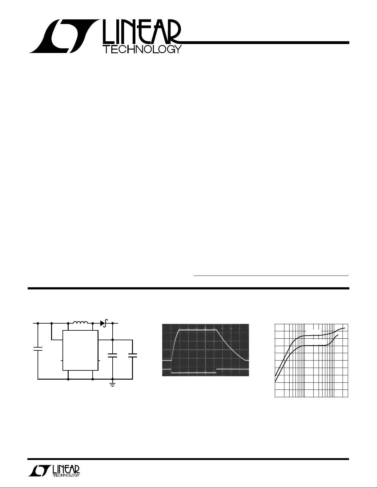
TYPICAL APPLICATIONS N
L1
V
IN
SELECT
SHDN
PGND
33µH
LT1301
5V
OR
+
C1
47µF
SHUTDOWN
*REQUIRED FOR 5V OUTPUT
L1 = COILCRAFT DO3316-333
OR SUMIDA CD73-330KC
D1 = 1N5817 OR MOTOROLA
MBRS130LT3
C1 = AVX TPSD476M016R0100
OR SANYO OS-CON 165A47M
C2 = AVX TPSD336M020R0100
OR SANYO OS-CON 205A33M
Figure 1. 3.3V/5V to 12V Step-Up Converter
SW
SENSE
I
LIM
GND
D1
N/C
+
12V
OUTPUT
C2
33µF
20V
LT1301 F1
0.1µF*
12V
V
OUT
2V/DIV
SHUTDOWN
10V/DIV
V
= 5V, V
IN
LOAD = 100Ω
Output Voltage
1ms/DIV
= 12V
OUT
Efficiency
LT1301 TAO1
LT1300 F2
1
Page 2
LT1301
WW
W
ABSOLUTE MAXIMUM RATINGS
VIN Voltage .............................................................. 10V
SW1 Voltage ............................................................ 20V
Sense Voltage .......................................................... 20V
Shutdown Voltage ................................................... 10V
Select Voltage .......................................................... 10V
I
Voltage ............................................................ 0.5V
LIM
Maximum Power Dissipation ............................. 500mW
Operating Temperature Range
LT1301C................................................... 0°C to 70°C
LT1301I .................................................. 40°C to 85°C
U
U
W
PACKAGE/ORDER INFORMATION
TOP VIEW
GND
1
SEL
2
SHDN
3
SENSE
4
N8 PACKAGE
8-LEAD PLASTIC DIP
T
= 100°C, θJA = 150°C/W
JMAX
PGND
8
SW
7
V
6
IN
I
5
LIM
S8 PACKAGE
8-LEAD PLASTIC SOIC
ORDER PART
NUMBER
LT1301CN8
LT1301CS8
LT1301IS8
S8 PART MARKING
1301
1301I
U
Storage Temperature Range ................. –65°C to 150°C
Lead Temperature (Soldering, 10 sec)..................300°C
ELECTRICAL CHARACTERISTICS
SYMBOL PARAMETER CONDITIONS MIN TYP MAX UNITS
I
Q
VINInput Voltage Range 1.8 V
V
OUT
DC Maximum Duty Cycle 75 86 95 %
t
ON
V
CESAT
V
SHDNH
V
SHDNL
V
SELH
V
SELL
I
SHDN
I
SEL
The ● denotes specifications which apply over the 0°C to 70°C
temperature range.
Quiescent Current V
Output Sense Voltage V
Output Referred V
Comparator Hysteresis V
Oscillator Frequency Current Limit not Asserted. 120 155 185 kHz
Oscillator TC 0.2 %/°C
Switch On-Time Current Limit not Asserted. 5.6 µs
Output Line Regulation 1.8V < VIN < 6V ● 0.06 0.15 %/V
Switch Saturation Voltage ISW = 700mA ● 130 200 mV
Switch Leakage Current VSW = 5V, Switch Off ● 0.1 10 µA
Peak Switch Current I
(Internal Trip Point) I
Shutdown Pin High ● 1.8 V
Shutdown Pin Low 0.5 V
Select Pin High ● 1.5 V
Select Pin Low ● 0.8 V
Shutdown Pin Bias Current V
Select Pin Bias Current 0V < V
= 0.5V, V
SHDN
V
= 1.8V ● 715 µA
SHDN
= 5V ● 11.52 12.00 12.48 V
SEL
V
= 0V ● 4.75 5.00 5.25 V
SEL
= 5V (Note 1) ● 50 100 mV
SEL
= 0V (Note 1) ● 22 50 mV
SEL
Floating (See Typical Application) 0.75 1.0 1.25 A
LIM
Grounded 0.4 A
LIM
= 5V ● 820 µA
SHDN
V
= 2V ● 3 µA
SHDN
V
= 0V ● 0.1 1 µA
SHDN
< 5V ● 13 µA
SEL
SEL
= 5V, V
TA = 25°C, V
= 5.5V ● 120 200 µA
SENSE
= 2V unless otherwise noted.
IN
● 2.0 V
Note 1: Hysteresis specified is DC. Output ripple may be higher if
output capacitance is insufficient or capacitor ESR is excessive.
See operation section.
2
Page 3
W
SHUTDOWN VOLTAGE (V)
0
SHUTDOWN CURRENT (µA)
0
4
6
8
20
12
14
2
4
5
LT1300 G3
2
16
18
10
13
6
7
8
T
A
= 25°C
U
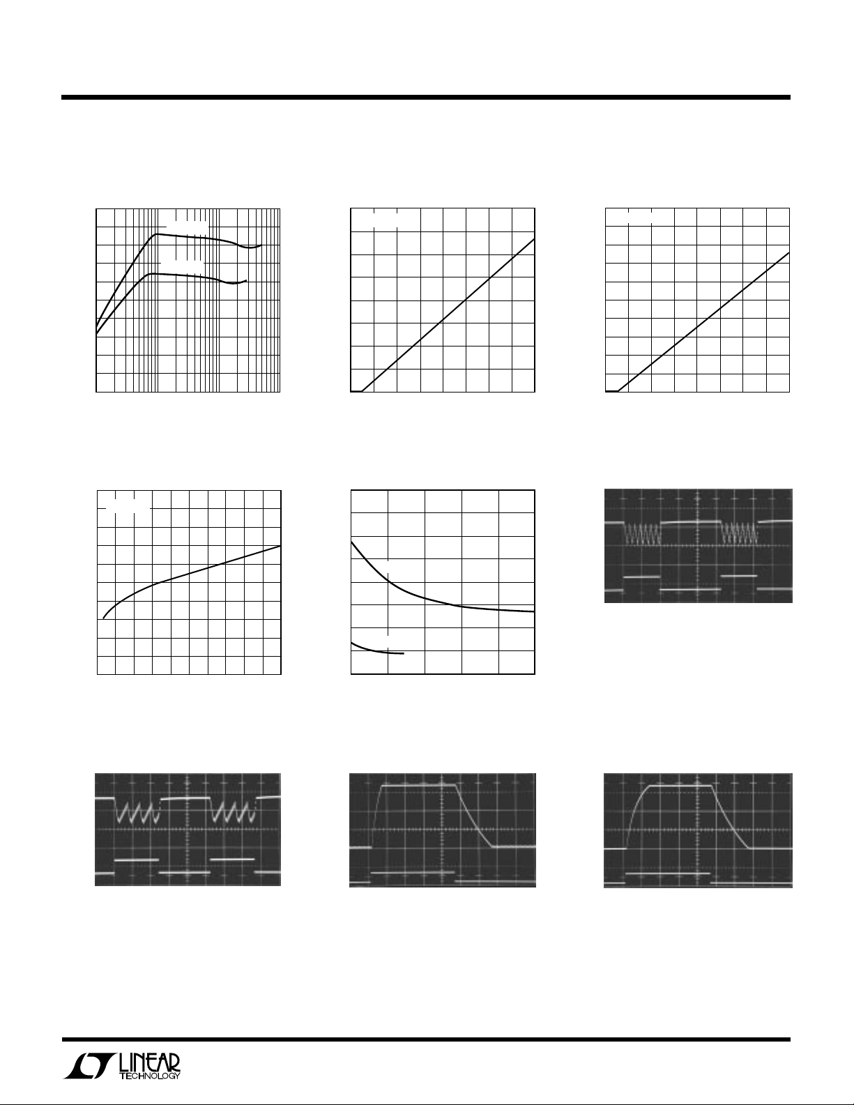
TYPICAL PERFORMANCE CHARACTERISTICS
Total Quiescent Current
5V Output Efficiency
90
88
86
84
82
80
78
EFFICIENCY (%)
76
74
72
70
1
VIN = 3.3V
VIN = 2.5V
10 100 1000
LOAD CURRENT (mA)
LT1301 G1
Saturation Voltage vs Switch Current No-Load Input Current
250
TA = 25°C
225
200
175
150
125
100
75
SATURATION VOLTAGE (mV)
50
25
0
0 0.1
0.2 0.3
SWITCH CURRENT (A)
0.4 0.5
0.6 0.7
0.8 0.9
LT1301 G4
1
in Shutdown
80
TA = 25°C
70
60
(µA)
50
SENSE
+ I
40
VIN
+ I
30
SHDN
I
20
10
0
1
0
500
450
400
350
300
250
INPUT CURRENT (µA)
200
150
100
2
2
V
OUT
= 5V
V
OUT
34 6
4
3
INPUT VOLTAGE (V)
= 12V
5
INPUT VOLTAGE (V)
5
6
7
LT1301 G2
LT1301 G5
8
AC COUPLED
I
7
V
OUT
100mV/DIV
120mA
LOAD
0mA
LT1301
Shutdown Pin Bias Current
Load Transient Response of
Figure 1 Circuit
VIN = 5V
200µs/DIV
LT1301 G6
Load Transient Response of
Figure 1 Circuit
V
OUT
100mV/DIV
AC COUPLED
120mA
I
LOAD
0mA
VIN = 3.3V
Select Pin Transient Response
12V
V
OUT
2V/DIV
5V
V
SELECT
200µs/DIV
LT1301 G7
10V/DIV
C
= 100µF, VIN = 5V
OUT
100Ω LOAD
5ms/DIV
LT1301 G8
Select Pin Transient Response
12V
V
OUT
2V/DIV
5V
V
SELECT
10V/DIV
5ms/DIV
C
= 100µF, VIN = 3.3V
OUT
100Ω LOAD
LT1301 G9
3
Page 4
LT1301
UUU
PIN FUNCTIONS
GND (Pin 1): Signal Ground. Tie to PGND under the
package.
Sel (Pin 2): Output Select. When tied to VIN converter
regulates at 12V. When grounded or floating converter
regulates at 5V. May be driven under logic control.
SHDN (Pin 3): Shutdown. Pull high to shut down the
LT1301. Ground for normal operation.
Sense (Pin 4): “Output” Pin. Goes to internal resistive
divider. If operating at 5V output, a 0.1µ F ceramic capacitor is required from Sense to Ground.
I
(Pin 5): Float for 1A switch current limit. Tie to ground
LIM
W
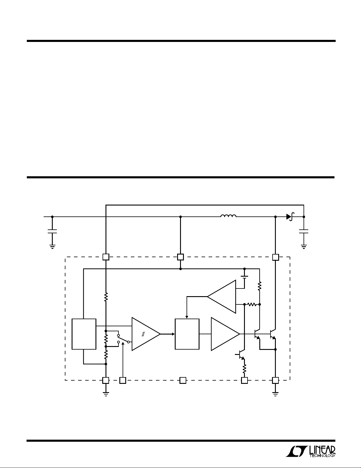
BLOCK DIAGRAM
V
IN
+
C1
for approximately 400mA. A resistor between I
LIM
and
ground sets peak current to some intermediate value .
VIN (Pin 6): Supply Pin. Must be bypassed with a large
value electrolytic to ground. Keep bypass within 0.2" of the
device.
SW (Pin 7): Switch Pin. Connect inductor and diode here.
Keep layout short and direct to minimize radio frequency
interference.
PGND (Pin 8): Power Ground. Tie to signal ground (pin 1)
under the package. Bypass capacitor from VIN should be
tied directly to PGND within 0.2" of the device.
L1
D1
V
OUT
+
C2
1.25V
REFERENCE
4
GND
1
SENSE
500k
97.5k
69.2k
SELECT
2
A1
COMPARATOR
+
–
ENABLE
V
IN
2
OFF
OSCILLATOR
155kHZ
SHUTDOWN
3
Figure 2.
A2 CURRENT
COMPARATOR
A3 DRIVER
BIAS
SW
7
18mV
+
R1
3Ω
R2
730Ω
–
Q1
Q2
160×
1×
Q3
8.5k
I
LIM
58
PGND
LT1301 F2
4
Page 5

S
TEST CIRCUIT
LT1301
5V
2V
SEL
V
IN
I
L
SW
100Ω
f
OUT
100µF
Oscillator Test Circuit
LT1301
SENSE
GND PGND
U
OPERATION
Operation of the LT1301 is best understood by referring to
the Block Diagram in Figure 2. When A1’s negative input,
related to the Sense pin voltage by the appropriate resistor-divider ratio is higher that the 1.25V reference voltage,
A1’s output is low. A2, A3 and the oscillator are turned off,
drawing no current. Only the reference and A1 consume
current, typically 120µ A. When A1’s negative input drops
below 1.25V, overcoming A1’s 6mV hysteresis, A1’s output goes high enabling the oscillator, current comparator
A2, and driver A3. Quiescent current increases to 2mA as
the device prepares for high current switching. Q1 then
turns on in controlled saturation for (nominally) 5.3µ s or
until comparator A2 trips, whichever comes first. After a
fixed off-time of (nominally) 1.2µ s, Q1 turns on again. The
LT1301’s switching causes current to alternately build up
in L1 and dump into output capacitor C2 via D1, increasing
the output voltage. When the output is high enough to
cause A1’s output to go to low, switching action ceases.
C2 is left to supply current to the load until V
enough to force A1’s output high, and the entire cycle
repeats. Figure 4 details relevant waveforms. A1’s cycling
causes low-to-mid-frequency ripple voltage on the output.
Ripple can be reduced by making the output capacitor
large. The 33µ F unit specified results in ripple of 100mV to
200mV on the 12V output. A 100µ F capacitor will decrease
ripple to 50mV. If operating at 5V ouput a 0.1µF ceramic
capacitor is required at the Sense pin in addition to the
electrolytic.
If switch current reaches 1A, causing A2 to trip, switch ontime is reduced and off-time increases slightly. This allows
continuous mode operation during bursts. A2 monitors
decreases
OUT
SHDN
LT1301 TC
the voltage across 3Ω resistor R1 which is directly related
to the switch current. Q2’s collector current is set by the
emitter-area ratio to 0.6% of Q1’s collector current. When
R1’s voltage drop exceeds 18mV, corresponding to 1A
switch current, A2’s output goes high, truncating the ontime portion of the oscillator cycle and increasing off-time
to about 2µs as shown in Figure 3, trace A. This pro-
grammed peak current can be reduced by tying the I
LIM
pin
to ground, causing 15µA to flow through R2 into Q3’s
collector. Q3’s current causes a 10.4mV drop in R2 so that
only an additional 7.6mV is required across R1 to turn off
the switch. This corresponds to a 400mA switch current
as shown in Figure 3, trace B. The reduced peak switch
current reduces I2R loses in Q1, L1, C1 and D1. Efficiency
can be increased by doing this provided that the accompanying reduction in full load current is acceptable. Lower
peak currents also extend alkaline battery life due to the
alkaline cell’s high internal impedance.
TRACE A
500mA/DIV
PIN
I
LIM
OPEN
TRACE B
500mA/DIV
PIN
I
LIM
GROUNDED
20µs/DIV
Figure 3. Switch Pin Current With I
Floating or Grounded
LIM
5
Page 6

LT1301
U
WUU
APPLICATIONS INFORMATION
V
OUT
100mV/DIV
AC COUPLED
V
SW
10V/DIV
I
L
500mA/DIV
20µs/DIV
V
IN
C
OUT
= 5V, V
OUT
= 33µF, I
= 12V, L = 33µH
= 90mA
LOAD
Figure 4. Burst Mode Operation in Action
Output Voltage Selection
The LT1301 can be selected to 5V or 12V under logic
control or fixed at either by tying Select to ground or V
respectively. It is permissible to tie Select to a voltage
higher than VIN as long as it does not exceed 10V.
Efficiency in 5V mode will be slightly less that in 12V mode
due to the fact that the diode drop is a greater percentage
of 5V than 12V. Since the bipolar switch in the LT1301 gets
its base drive from VIN, no reduction in switch efficiency
occurs when in 5V mode. When VIN exceeds the programmed output voltage the output will follow the input.
This is characteristic of the simple step-up or “boost”
converter topology. A circuit example that provides a
regulated output with an input voltage above or below the
output (known as a buck-boost or SEPIC) is shown in the
Typical Applications section.
Shutdown
The converter can be turned off by pulling SHDN (pin 3)
high. Quiescent current drops to 10µA in this condition.
Bias current of 8µ A to 10µ A flows into the pin (at 5V input).
It is recommended that SHDN not be left floating. Tie the
pin to ground if the feature is not used. SHDN can be driven
high even if VIN is floating.
I
Function
LIM
The LT1301’s current limit (I
) pin can be used for soft
LIM
start. Upon start-up, the LT1301 will draw maximum
current from the supply (about 1A) from the supply to
charge the output capacitor. Figure 5 shows V
waveforms as the device is turned on. The high current
flow can create IR drops along supply and ground lines
or cause the input supply to drop out momentarily. By
LT1300 F4
OUT
and I
IN
IN
V
OUT
5V/DIV
I
IN
500mA/DIV
V
SHDN
10V/DIV
V
IN
= 5V, V
OUT
200µs/DIV
= 12V
LT1300 F5
Figure 5. Start-Up Response
D1
1N5817
R1
1M
C3
0.1µF
+
LT1301 F6
12V
C2
33µF
V
3.3V OR 5V
IN
+
47µF
SHUTDOWN
V
IN
SELECT
SHDN
GND
L1
33µH
LT1301
SW
SENSE
I
LIM
PGND
Figure 6.
V
OUT
5VDIV
I
IN
500mA/DIV
V
SHDN
10V/DIV
VIN = 5V, V
OUT
200µs/DIV
= 12V
LT1300 F5
Figure 7. Startup Response Soft-Start Circuitry Added
adding R1 and C3 as shown in Figure 6, the switch
current in the LT1301 is initially limited to 400mA until
the 15µ A flowing out of the I
pin charges up C3. Input
LIM
current is held to under 500mA while the output voltage
ramps up to 12V as shown in Figure 7. R1 provides a
discharge path for the capacitor without appreciably decreasing peak switch current. When using the I
pin soft-
LIM
start mode a minimum load of a few hundred microamperes is recommended to prevent C3 from discharging, as
no current flows out of I
when the LT1301 is not
LIM
6
Page 7

LT1301
U
WUU
APPLICATIONS INFORMATION
Table 1. Recommended Inductors
EFFICIENCY (%) COMPONENT
PART NUMBER VENDOR L (µH) DCR (Ω)VIN(V) I
DO3316-333 Coilcraft 33 0.088 3.3 Open 84 84 85 5.5 (708) 639–6400
5 Open 89 89 90
DO1608-223 Coilcraft 22 .31 3.3 Open 82 82 — 3.5
3.3 Ground 85 — —
5 10k 86 87 —
5 Ground 88 — —
DO1608-103 Coilcraft 10 .11 2 Open 78 — — 3.5
CTX20-1 Coiltronics 20 .175 3.3 Open 84 84 — 4.2 (407) 241-7876
5 Open 88 88 89
GA10-332 Gowanda 33 .077 3.3 Open 86 86 87 Through-Hole (716) 532-2234
5 Open 89 89 90
LQH3G220K04M00 Murata-Erie 22 0.7 3.3 Ground 81 — — 2.0 (404) 436-1300
5 Ground 85 — —
CD73-330KC Sumida 33 0.131 3.3 Open 84 85 86 3.5 (708) 956-0666
5 Open 88 88 89
CDRH62-330MC Sumida 33 0.48 3.3 Open 80 80 81 3.0
5 Open 84 84 85
PIN 30mA 60mA 120mA HEIGHT (mm) PHONE NUMBER
LIM
Ground 85 — —
Ground 83 — —
switching. Zero load current causes the LT1301 to switch
so infrequently that C3 can completely discharge reducing
subsequent peak switch current to 400mA. If a load is
suddenly applied, output voltage will sag until C3 can be
recharged and peak switch current returns to 1A.
If the full capacity of the LT1301 is not required peak
current can be reduced by changing the value of R3 as
shown in Figure 8. With R3 = 0 switch current is limited to
approximately 400mA. Smaller, less expensive inductors
with lower saturation ratings can then be used.
Inductor Selection
For full output power, the inductor should have a saturation current rating of 1.25A for worst-case current limit,
although it is acceptable to bias an inductor 20% or more
into saturation. Smaller inductors can be used in conjunction with the I
pin. Efficiency is significantly affected by
LIM
inductor DCR. For best efficiency limit the DCR to 0.03Ω
or less. Toroidal types are preferred in some cases due to
their inherent flux containment and EMI/RFI superiority.
Recommended inductors are listed in Table 1.
Table 2. Recommended Capacitors
VENDOR SERIES TYPE PHONE#
AVX TPS Surface Mount (803)448–9411
Sanyo OS-CON Through-Hole (619) 661–6835
Panasonic HFQ Through-Hole (201) 348-5200
1100
1.6V ≤ VIN ≤ 5V
1000
900
800
700
600
SWITCH CURRENT (mA)
500
400
300
100 10k 100k 1M
Figure 8. Peak Switch Current vs. Current Limit Set Resistor
1k
CURRENT LIMIT SET RESISTOR (Ω)
LT1301 F8
7
Page 8

LT1301
U
WUU
APPLICATIONS INFORMATION
Capacitor Selection
Low ESR capacitors are required for both input and output
of the LT1301. ESR directly affects ripple voltage and
efficiency. For surface mount applications AVX TPS series
tantalum capacitors are recommended. These have been
specially designed for SMPS and have low ESR along with
high surge current ratings. For through-hole applications
Sanyo OS-CON capacitors offer extremely low ESR in a
small size. Again, if peak switch current is reduced using
the I
pin, capacitor requirements can be relaxed and
LIM
smaller, higher ESR units can be used. Suggested capacitor sources are listed in Table 2.
U
TYPICAL APPLICATIONS N
Diode Selection
Best performance is obtained with a Schottky rectifier
diode such as the 1N5817. Phillips Components makes
this in surface mount as the PRLL5817. Motorola makes
the MBRS130LT3 which is slightly better and also in
surface mount. For lower output power a 1N4148 can be
used although efficiency will suffer substantially.
Layout Considerations
The LT1301 is a high speed, high current device. The input
capacitor must be no more than 0.2˝ from VIN (pin 6) and
ground. Connect the PGND and GND (pins 8 and 1)
together under the package. Place the inductor adjacent to
SW (pin 7) and make the switch pin trace as short as
possible. This keeps radiated noise to a minimum.
4 CELLS
2×
AA
CELL
Four-Cell to 5V Converter
C2
100µF
+
0.1µF
+
C1
100µF
SHUTDOWN
NC
V
IN
I
LIM
SHDN
GND
L1
33µH
LT1301
SW
SENSE
SELECT
PGND
Step-Up Converter with Automatic Output Disconnect
+
SHUTDOWN
100µF
NC
NC
SELECT
SHDN
I
LIM
GND
LT1301
V
SW
SENSE
PGND
L1*
10µH
IN
1N5817
L2
33µH
470Ω
+
1N5817
100µF
LT1301 TAO3
2N4403
5V OUTPUT
200mA
80 to 83% EFFICIENT
> 10mA
AT I
LOAD
+
C3
100µF
5V, 200mA
0.1µF
8
*SUMIDA CD54-100LC
COILCRAFT DO3316-223
LT1301 TA4
Page 9

U
TYPICAL APPLICATIONS N
V
IN
1.8V TO 6V
LCD Contrast Supply
T1
4
7
1
3
10
8
2
9
1N5819
150K
CONTRAST
V
–4V TO –29V 12mA
OUT
MAXIMUM FROM 1.8V SUPPLY
(77% EFFICIENT)
20mA MAXIMUM FROM
3V SUPPLY (83% EFFICIENT)
22µF
35V
+
LT1301
V
2V - 6V
V
IN
SENSE
NC
+
100µF
NC
T1 = DALE LPE-5047-AO45 (605) 665-9301
LT1301
SELECT
PGND
SW
SHDN
I
LIM
GND
SHUTDOWN
CMOS DRIVE 0V TO 5V
12K
12K
PWM IN
0% TO 100%
+
2.2µF
LT1300 TA5
Low-Voltage CCFL Power Supply
97
IN
1Ω
1N5817
1µF
L1
47µH
7.5K
1%
2N3904
0.1µF
NC
V
IN
SENSE
SHDN
GND
LT1301
SELECT
SW
I
LIM
PGND
+
15TI4
120Ω
1N4148
32
0.068µF
WIMA
MKP20
+
10µF
ZTX849ZTX849
22pF
3kV
CCFL
SHUTDOWN
T1 = COILTRONICS CTX110654-1
L1 = COILCRAFT D03316-473
0 - 5VDC IN
INTENSITY ADJUST
100µA TO 2mA BULB CURRENT
LT1300 TA6
9
Page 10

LT1301
U
TYPICAL APPLICATIONS N
5V
+
33µF
0.1µF
5V to –5V Converter
V
IN
SELECT
NC
SENSENC
GND
LT1301
LT1300
1N4148
OR
2
1
SW
SHDN
I
PGND
L1
33µH
LIM
3
4
SHUTDOWN
–V
5V
OUT
300mA
33µF
1N58171N965
4.99K
1%
+
4.99K
1%
L1 = COILTRONICS CTX33-4
5V
LT1301 TA7
10
Page 11

PACKAGE DESCRIPTION
0.300 – 0.320
(7.620 – 8.128)
U
Dimensions in inches (millimeters) unless otherwise noted.
N8 Package
8-Lead Plastic DIP
0.400
0.045 – 0.065
(1.143 – 1.651)
0.130 ± 0.005
(3.302 ± 0.127)
(10.160)
MAX
876
LT1301
5
0.008 – 0.010
(0.203 – 0.254)
0.065
(1.651)
0.009 – 0.015
(0.229 – 0.381)
+0.025
0.325
–0.015
+0.635
8.255
()
–0.381
TYP
0.045 ± 0.015
(1.143 ± 0.381)
0.100 ± 0.010
(2.540 ± 0.254)
8-Lead Plastic S0IC
0.010 – 0.020
(0.254 – 0.508)
× 45°
0°– 8° TYP
0.016 – 0.050
0.406 – 1.270
*THESE DIMENSIONS DO NOT INCLUDE MOLD FLASH OR PROTRUSIONS.
MOLD FLASH OR PROTRUSIONS SHALL NOT EXCEED 0.006 INCH (0.15mm).
0.053 – 0.069
(1.346 – 1.752)
0.014 – 0.019
(0.355 – 0.483)
0.018 ± 0.003
(0.457 ± 0.076)
S8 Package
0.050
(1.270)
BSC
0.125
(3.175)
MIN
0.004 – 0.010
(0.101 – 0.254)
0.020
(0.508)
MIN
0.228 – 0.244
(5.791 – 6.197)
1234
0.189 – 0.197*
(4.801 – 5.004)
7
8
1
6
3
2
0.250 ± 0.010
(6.350 ± 0.254)
5
0.150 – 0.
(3.810 – 3.
4
N8 0392
SO8 0294
Information furnished by Linear Technology Corporation is believed to be accurate and reliable.
However, no responsibility is assumed for its use. Linear Technology Corporation makes no representation that the interconnection of its circuits as described herein will not infringe on existing patent rights.
11
Page 12

LT1301
U.S. Area Sales Offices
NORTHEAST REGION
Linear Technology Corporation
One Oxford Valley
2300 E. Lincoln Hwy.,Suite 306
Langhorne, PA 19047
Phone: (215) 757-8578
FAX: (215) 757-5631
Linear Technology Corporation
266 Lowell St., Suite B-8
Wilmington, MA 01887
Phone: (508) 658-3881
FAX: (508) 658-2701
FRANCE
Linear Technology S.A.R.L.
Immeuble "Le Quartz"
58 Chemin de la Justice
92290 Chatenay Malabry
France
Phone: 33-1-41079555
FAX: 33-1-46314613
SOUTHEAST REGION
Linear Technology Corporation
17060 Dallas Parkway
Suite 208
Dallas, TX 75248
Phone: (214) 733-3071
FAX: (214) 380-5138
CENTRAL REGION
Linear Technology Corporation
Chesapeake Square
229 Mitchell Court, Suite A-25
Addison, IL 60101
Phone: (708) 620-6910
FAX: (708) 620-6977
International Sales Offices
KOREA
Linear Technology Korea Branch
Namsong Building, #505
Itaewon-Dong 260-199
Yongsan-Ku, Seoul
Korea
Phone: 82-2-792-1617
FAX: 82-2-792-1619
SOUTHWEST REGION
Linear Technology Corporation
22141 Ventura Blvd.
Suite 206
Woodland Hills, CA 91364
Phone: (818) 703-0835
FAX: (818) 703-0517
NORTHWEST REGION
Linear Technology Corporation
782 Sycamore Dr.
Milpitas, CA 95035
Phone: (408) 428-2050
FAX: (408) 432-6331
TAIWAN
Linear Technology Corporation
Rm. 801, No. 46, Sec. 2
Chung Shan N. Rd.
Taipei, Taiwan, R.O.C.
Phone: 886-2-521-7575
FAX: 886-2-562-2285
GERMANY
Linear Techonolgy GmbH
Untere Hauptstr. 9
D-85386 Eching
Germany
Phone: 49-89-3197410
FAX: 49-89-3194821
JAPAN
Linear Technology KK
5F YZ Bldg.
4-4-12 Iidabashi, Chiyoda-Ku
Tokyo, 102 Japan
Phone: 81-3-3237-7891
FAX: 81-3-3237-8010
SINGAPORE
Linear Technology Pte. Ltd.
101 Boon Keng Road
#02-15 Kallang Ind. Estates
Singapore 1233
Phone: 65-293-5322
FAX: 65-292-0398
World Headquarters
Linear Technology Corporation
1630 McCarthy Blvd.
Milpitas, CA 95035-7487
Phone: (408) 432-1900
FAX: (408) 434-0507
UNITED KINGDOM
Linear Technology (UK) Ltd.
The Coliseum, Riverside Way
Camberley, Surrey GU15 3YL
United Kingdom
Phone: 44-276-677676
FAX: 44-276-64851
08/16/93
12
Linear Technology Corporation
1630 McCarthy Blvd., Milpitas, CA 95035-7487
(408) 432-1900
●
FAX
: (408) 434-0507
●
TELEX
: 499-3977
LT/GP 0394 10K • PRINTED IN USA
LINEAR TECHNOLOGY CORPORATION 1994
 Loading...