

Page 1
3.3/5V Step-Up DC/DC Converter
FEATURES
■
Up to 220mA Output Current at 5V from 2V Supply
■
Supply Voltage as Low as 1.8V
■
Up to 88% Efficiency
■
Small Inductor –10µH
■
120µA Quiescent Current
■
Shutdown to 10µA
■
Programmable 3.3V or 5V Output
■
I
Pin Programs Peak Switch Current
LIM
■
Low V
■
Uses Inexpensive Surface Mount Inductors
■
8-Lead DIP or SOIC Package
Switch: 170mV at 1A Typical
CESAT
U
APPLICATIONS
■
Palmtop Computers
■
Portable Instruments
■
Bar-Code Scanners
■
DC/DC Converter Module Replacements
■
Battery Backup Supplies
■
Personal Digital Assistants
■
PCMCIA Cards
LT1300
Micropower High Efficiency
U
DESCRIPTION
The LT1300 is a micropower step-up DC/DC converter that
utilizes Burst Mode™ operation. The device can deliver 5V
or 3.3V from a two-cell battery input. It features programmable 5V or 3.3V output via a logic-controlled input, noload quiescent current of 120µ A and a shutdown pin which
reduces supply current to 10µ A. The on-chip power switch
has a low 170mV saturation voltage at a switch current of
1A, a four-fold reduction over prior designs. A 155kHz
internal oscillator allows the use of extremely small surface mount inductors and capacitors. Operation is guaranteed at 1.8V input. This allows more energy to be extracted
from the battery increasing operating life. The I
be used to program peak switch current with a single
resistor allowing the use of less expensive and smaller
inductors and capacitors in lighter load applications. The
LT1300 is available in an 8-lead SOIC package, minimizing
board space requirements. For a 5V/12V Selectable Output Converter see the LT1301. For increased output current see the LT1302.
Burst Mode is a trademark of Linear Technology Corporation.
LIM
pin can
U
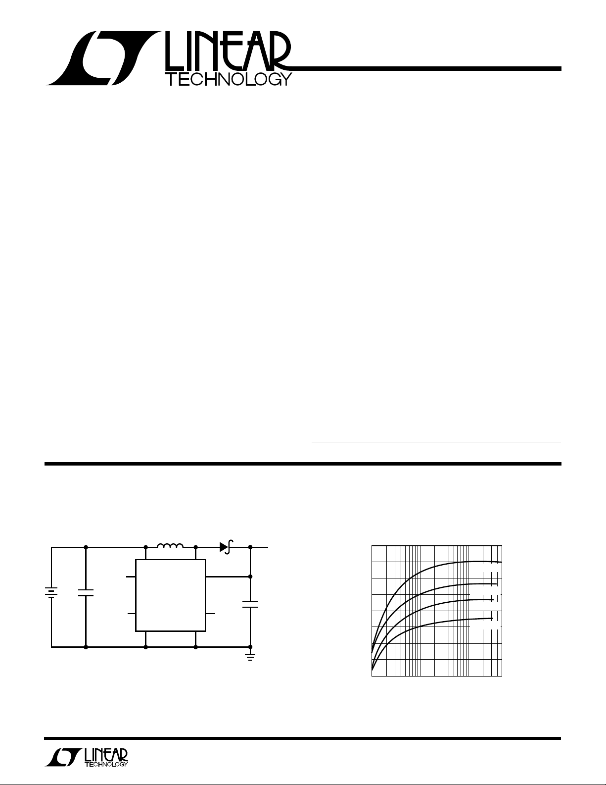
TYPICAL APPLICATIONS N
Two-Cell to 3.3V/5V Step-Up Converter 5V Output Efficiency
L1
10µH D1
5V/3.3V
2×
AA
CELL
L1 = COILCRAFT DO1608-103
OR SUMIDA CD54-100
C1 = AVX TPSD107M010R0100
OR SANYO OS-CON 16SA100M
D1 =MBRS130LT3
OR 1N5817
SELECT
+
C1
100µF
SHUTDOWN
67
V
IN
2
SELECT
LT1300
3
SHDN
PGND
81
SW
SENSE
I
LIM
GND
4
5
N/C
+
C1
100µF
5V/3.3V
OUTPUT
LT1300 TA1
90
88
86
84
82
80
EFFICIENCY (%)
78
76
74
1
VIN = 4.0V
VIN = 3.0V
VIN = 2.5V
VIN = 2.0V
10 100 500
LOAD CURRENT (mA)
LT1300 TA2
1
Page 2
LT1300
WW
W
ABSOLUTE MAXIMUM RATINGS
VIN Voltage .............................................................. 10V
SW1 Voltage ............................................................ 20V
Sense Voltage .......................................................... 10V
SHUTDOWN Voltage................................................ 10V
SELECT Voltage ....................................................... 10V
I
Voltage ............................................................ 0.5V
LIM
Maximum Power Dissipation ............................. 500mW
Operating Temperature Range ..................... 0°C to 70°C
Storage Temperature Range ................. –65°C to 150°C
U
U
W
PACKAGE/ORDER INFORMATION
TOP VIEW
GND
1
SEL
2
SHDN
3
SENSE
4
N8 PACKAGE
8-LEAD PLASTIC DIP
T
= 100°C, θJA = 150°C/W
JMAX
PGND
8
SW
7
V
6
IN
I
5
LIM
S8 PACKAGE
8-LEAD PLASTIC SOIC
ORDER PART
NUMBER
LT1300CN8
LT1300CS8
S8 PART MARKING
1300
U
Lead Temperature (Soldering, 10 sec).................. 300°C
Consult factory for Industrial grade parts.
SEL
= 5V, V
TA = 25°C, V
SENSE
ELECTRICAL CHARACTERISTICS
SYMBOL PARAMETER CONDITIONS MIN TYP MAX UNITS
I
Q
VINInput Voltage Range 1.8 V
V
OUT
DC Maximum Duty Cycle 75 86 95 %
t
ON
V
CESAT
V
SHDNH
V
SHDNL
V
SELH
V
SELL
I
SHDN
I
SEL
The
temperature range.
Quiescent Current V
Output Sense Voltage V
Output Referred V
Comparator Hysteresis V
Oscillator Frequency Current Limit not Asserted. See Test Circuit. 120 155 185 kHz
Oscillator TC 0.2 %/°C
Switch On Time Current Limit not Asserted. 5.6 µs
Output Line Regulation 1.8V < VIN < 6V ● 0.06 0.15 %/V
Switch Saturation Voltage ISW = 700mA ● 130 200 mV
Switch Leakage Current VSW = 5V, Switch Off ● 0.1 10 µA
Peak Switch Current I
(Internal Trip Point) I
Shutdown Pin High ● 1.8 V
Shutdown Pin Low 0.5 V
Select Pin High ● 1.5 V
Select Pin Low ● 0.8 V
Shutdown Pin Bias Current V
Select Pin Bias Current 0V < V
● denotes specifications which apply over the 0°C to 70°C
= 0.5V, V
SHDN
V
= 1.8V ● 715 µA
SHDN
= 5V ● 4.80 5.0 5.20 V
SEL
V
= 0V ● 3.15 3.3 3.45 V
SEL
= 5V (Note 1) ● 22 50 mV
SEL
= 0V (Note 1) ● 14 35 mV
SEL
Floating (See Typical Application) 0.75 1.0 1.25 A
LIM
Grounded 0.4 A
LIM
= 5V ● 920 µA
SHDN
= 2V ● 3 µA
V
SHDN
V
= 0V ● 0.1 1 µA
SHDN
< 5V ● 13 µA
SEL
= 2V unless otherwise noted.
IN
= 5.5V ● 120 200 µA
● 2.0 V
Note 1: Hysteresis specified is DC. Output ripple may be higher if
output capacitance is insufficient or capacitor ESR is excessive. See
applications section.
2
Page 3
W
INPUT VOLTAGE (V)
0
I
SHDN
+ I
VIN
+ I
SENSE
(µA)
40
50
60
8
LT1300 G3
30
20
0
2
4
6
10
80
70
1
3
5
7
INPUT VOLTAGE (V)
1.5
OUTPUT CURRENT (mA)
500
600
700
34
LT1300 G6
400
300
2
2.5
3.5 4.5
200
100
0
V
OUT
= 5V,
I
LIM
FLOATING
L = 22µH
COILCRAFT
DO3316-223
L = 10µH
COILCRAFT
DO1608-103
U
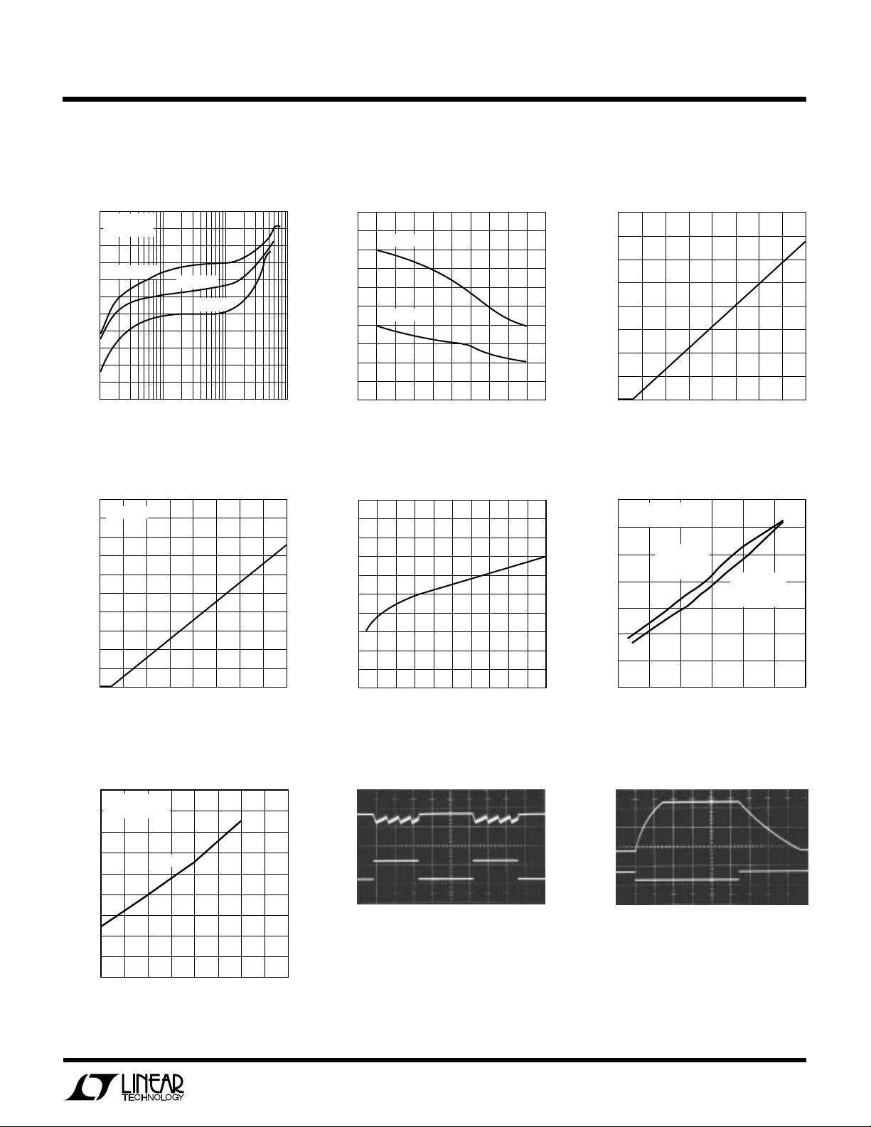
TYPICAL PERFORMANCE CHARACTERISTICS
Efficiency
88
V
= 3.3V
OUT
86
L = 10µH
84
82
VIN = 3V
80
78
76
74
EFFICIENCY (%)
72
70
68
66
1
VIN = 2.5V
10 100 1000
LOAD CURRENT (mA)
Shutdown Pin Bias Current
20
T
= 25°C
A
18
16
14
12
10
8
6
SHUTDOWN CURRENT (µA)
4
2
0
0
13
2
SHUTDOWN VOLTAGE (V)
VIN = 2V
4
5
LT1300 G1
7
6
LT1300 G4
8
No-Load Battery Current
170
165
160
155
150
145
140
135
INPUT CURRENT (µA)
130
125
120
250
225
200
175
150
(mV)
125
CESAT
100
V
75
50
25
1.4
V
0
CESAT
0 0.1
V
= 5V
OUT
V
= 3.3V
OUT
1.81.6
2.22.0
INPUT VOLTAGE (V)
vs I
SW
0.2 0.3
0.4 0.5
SWITCH CURRENT (A)
2.62.4
0.6 0.7
3.02.8
0.8 0.9
LT1300
Total Quiescent Current
in Shutdown
3.43.2
LT1300 G2
Maximum Output Current
vs Input Voltage
1
LT1300 G5
Maximum Output Current
vs Input Voltage
900
800
700
600
500
400
300
LOAD CURRENT (mA)
200
100
0
1.5
V
= 3.3V
OUT
I
FLOATING
LIM
L = 10µH
2
2.5
INPUT VOLTAGE (V)
Transient Response
VIN = 2V, V
V
OUT
100mV/DIV
AC COUPLED
200mA
I
LOAD
0
3.5
3
LT1300 G7
OUT
200µs/DIV
= 5V
LT1300 G8
Startup Response
V
OUT
1V/DIV
V
SHDN
10V/DIV
V
= 5V
OUT
= 20Ω
R
LOAD
500µs/DIV
LT1300 G9
3
Page 4

LT1300
PIN FUNCTIONS
UUU
GND (Pin 1): Signal Ground.
Sel (Pin 2): Output Select. When tied to VIN or V
OUT
converter regulates at 5V. When grounded converter
regulates at 3.3V.
SHDN (Pin 3): Shutdown. Pull high to effect shutdown. Tie
to ground for normal operation.
Sense (Pin 4): “Output” Pin.
I
(Pin 5): Float for 1A switch current limit. Tie to ground
LIM
for approximately 400mA. A resistor between I
LIM
and
ground sets peak current to some intermediate value (see
Figure 5).
W
BLOCK DIAGRAM
V
IN
+
C1
VIN (Pin 6): Supply Pin. Must be bypassed with a large
value electrolytic to ground. A 0.1µF ceramic capacitor
close to the pin may be needed in some cases.
SW (Pin 7): Switch Pin. Connect inductor and diode here.
Keep layout short and direct to minimize electronic radiation.
PGND (Pin 8): Power Ground. Tie to signal ground (pin 1)
under the package. Bypass capacitor from VIN should be
tied directly to the pin.
L1
D1
V
OUT
+
C2
1.25V
REFERENCE
SENSE
4
144k
GND
1
500k
161k
SELECT
2
A1
COMPARATOR
+
–
ENABLE
Figure 1.
V
IN
2
OSCILLATOR
155kHZ
SHUTDOWN
3
A2 CURRENT
COMPARATOR
OFF
A3 DRIVER
BIAS
SW
7
18mV
R2
730Ω
R1
3Ω
+
–
Q1
Q2
160x
1x
Q3
8.5k
I
LIM
58
PGND
LT1300 F1
4
Page 5

S
TEST CIRCUIT
LT1300
Oscillator Test Circuit
2V
SEL
V
IN
I
L
SW
5V
100Ω
f
OUT
100µF
LT1300
SENSE
GND PGND
U
OPERATION
Operation of the LT1300 is best understood by referring to
the Block Diagram in Figure 1. When A1’s negative input,
related to the Sense pin voltage by the appropriate resistor-divider ratio, is higher that the 1.25V reference voltage,
A1’s output is low. A2, A3 and the oscillator are turned off,
drawing no current. Only the reference and A1 consume
current, typically 120µA. When the voltage at A1’s nega-
tive input decreases below 1.25V, overcoming A1’s 6mV
hysteresis, A1’s output goes high, enabling the oscillator,
current comparator A2, and driver A3. Quiescent current
increases to 2mA as the device prepares for high current
switching. Q1 then turns on in a controlled saturation for
(nominally) 5.3µs or until current comparator A2 trips,
whichever comes first. After a fixed off-time of (nominally)
1.2µ s, Q1 turns on again. The LT1300’s switching causes
current to alternately build up in L1 and dump into capacitor C2 via D1, increasing the output voltage. When the
output is high enough to cause A1’s output to go to low,
switching action ceases. C2 is left to supply current to the
load until V
high, and the entire cycle repeats.
If switch current reaches 1A, causing A2 to trip, switch ontime is reduced and off-time increases slightly. This allows
continuous mode operation during bursts. Current comparator A2 monitors the voltage across 3Ω resistor R1
which is directly related to inductor L1’s current. Q2’s
collector current is set by the emitter-area ratio to 0.6%
of Q1’s collector current. When R1’s voltage drop exceeds
18mV, corresponding to 1A inductor current, A2’s output
goes high, truncating the on-time portion of the oscillator
cycle and increasing off-time to about 2µs as shown in
Figure 2, trace A. This programmed peak current can be
decreases enough to force A1’s output
OUT
SHDN
TRACE A
500mA/DIV
PIN
I
LIM
OPEN
TRACE B
500mA/DIV
PIN
I
LIM
GROUNDED
20µs/DIV
Figure 2. Switch Pin Current With I
reduced by tying the I
pin to ground, causing 15µA to
LIM
Floating or Grounded
LIM
LT1300 F2
flow through R2 into Q3’s collector. Q3’s current causes
a 10.4mV drop in R2 so that only an additional 7.6mV is
required across R1 to turn off the switch. This corresponds to a 400mA switch current as shown in Figure 2,
trace B. The reduced peak switch current reduces I2R
loses in Q1, L1, C1 and D1. Efficiency can be increased by
doing this provided that the accompanying reduction in
full load output current is acceptable. Lower peak currents
also extend alkaline battery life due to the alkaline cell’s
high internal impedance. Typical operating waveforms are
shown in Figure 3.
V
OUT
20mV/DIV
AC COUPLED
V
SW
5V/DIV
I
SW
IA/DIV
20µS/DIV
Figure 3. Burst Mode Operation in Action
LT1300 F2
5
Page 6

LT1300
U
WUU
APPLICATIONS INFORMATION
Output Voltage Selection
The LT1300 can be selected to 3.3V or 5V under logic
control or fixed at either by tying SELECT to ground or V
respectively. It is permissible to tie SELECT to a voltage
higher than VIN as long as it does not exceed 10V.
Efficiency in 3.3V mode will be slightly less that in 5V mode
due to the fact that the diode drop is a greater percentage
of 3.3V than 5V. Since the bipolar switch in the LT1300
gets its base drive from VIN, no reduction in switch
efficiency occurs when in 3.3V mode. When VIN exceeds
the programmed output voltage the output will follow the
input. This is characteristic of the simple step-up or
“boost” converter topology. A circuit example that provides a regulated output with an input voltage above or
below the output (called a buck-boost or SEPIC) is shown
in the Typical Applications section.
Shutdown
The converter can be turned off by pulling SHDN (pin 3)
high. Quiescent current drops to 10µA in this condition.
Bias current of 3µA to 5µ A flows into the pin (at 2.5V input).
It is recommended that SHDN not be left floating. Tie the
pin to ground if the feature is not used.
IN
L1
10µH
V
IN
+
SELECT
C1
100µF
SHDN
PGND GND
LT1300
SW
SENSE
I
LIM
R1
1M
D1
5V/3.3V
OUTPUT
+
C2
100µF
C3
0.1µF
Figure 4. Addition of R1 and C3 Limit Input Current at Startup
V
OUT
2VDIV
I
BATTERY
500mA/DIV
V
SHDN
10V/DIV
500µs/DIV
REP RATE = 1Hz
LT1300 F5
I
Function
LIM
The LT1300’s current limit (I
) pin can be used for soft
LIM
start. Upon start-up, switching regulators require maximum current from the supply. The high currents flowing
can create IR drops along supply and ground lines and
are especially demanding on alkaline batteries. By installing an R1 and C3 as shown in Figure 4, the switch
current in the LT1300 is limited to 400mA until the 15µ A
flowing out of the I
pin charges up the 0.1µ F capaci-
LIM
tor. Input current is held to under 500mA while the
output voltage ramps up to 5V as shown in Figure 5. The
1Meg resistor provides a discharge path for the capacitor
without appreciably decreasing peak switch current. When
the full capability of the LT1300 is not required, peak
current can be reduced by changing the value of R3 as
shown in Figure 6. With R3 = 0, switch current is limited
to approximately 400mA.
Figure 5. Startup Waveforms using Soft-Start Circuitry
I
= 100mA, V
LOAD
1100
1.6V ≤ VIN ≤ 5V
1000
900
800
700
600
SWITCH CURRENT (mA)
500
400
300
100 10k 100k 1M
1k
Figure 6. Peak Switch Current vs. R
R
OUT
LIM
= 5V
(Ω)
LT1300 F1B
LIM
6
Page 7

LT1300
U
WUU
APPLICATIONS INFORMATION
Table 1. Recommended Inductors
EFFICIENCY 2.5VIN, 5V
PART NUMBER VENDOR L (µH) DCR (Ω)I
DO1608-103 Coilcraft 10 0.11 Float 83 83 3.5 (708) 639–6400
DO3316-223 Coilcraft 22 0.050 Float 85 85 5.5
DO1608-223 Coilcraft 22 0.31 Ground 85 — 3.5
CTX10-1 Coiltronics 10 0.038 Float 85 85 4.2 (407) 241–7876
CTX20-1 Coiltronics 20 0.175 Ground 86 — 4.2
LQH3C2204K0M00 Murata-Frie 22 0.7 Ground 81 — 2.0 (404) 436–1300
CD54-100M Sumida 10 0.11 Float 85 85 4.5 (708) 956–0666
CDRH62-220M Sumida 22 0.38 Ground 84 — 3.0
CDRH62-100M Sumida 10 0.17 Float 81 82 3.0
GA10-102K Gowanda 10 0.038 Float 85 86 6.6 Through-Hole (716) 532–2234
Inductor Selection
For full output power, the inductor should have a saturation current rating of 1.25A for worst-case current limit,
although it is acceptable to bias an inductor 20% or more
into saturation. Smaller inductors can be used in conjunction with the I
pin. Efficiency is significantly affected by
LIM
inductor DCR. For best efficiency limit the DCR to 0.03Ω
or less. Toroidal types are preferred in some cases due to
their closed design and inherent EMI/RFI superiority.
Recommended inductors are listed in Table 1.
PIN 50mA LOAD 200mA LOAD HEIGHT (mm) PHONE NUMBER
LIM
Table 2. Recommended Capacitors
VENDOR SERIES TYPE PHONE#
AVX TPS Surface Mount (803)448–9411
Sanyo OS-CON Through-Hole (619) 661–6835
Panasonic HFQ Through-Hole (201) 348–5200
Diode Selection
Best performance is obtained with a Schottky rectifier
diode such as the 1N5817. Phillips Components makes
this in surface mount as the PRLL5817. Motorola makes
the MBRS130LT3 which is slightly better and also in
Capacitor Selection
Low ESR capacitors are required for both input and output
surface mount. For lower output power a 1N4148 can be
used although efficiency will suffer substantially.
of the LT1300. ESR directly affects ripple voltage and
efficiency. For surface mount applications AVX TPS series
tantalum capacitors are recommended. These have been
specially designed for SMPS and have low ESR along with
high surge current ratings. For through-hole application
Sanyo OS-CON capacitors offer extremely low ESR in a
small size. Again, if peak switch current is reduced using
the I
pin, capacitor requirements can be relaxed and
LIM
Layout Considerations
The LT1300 is a high speed, high current device. The input
capacitor must be no more than 0.2" from VIN (pin 6) and
ground. Connect the PGND and GND (pins 8 and 1)
together under the package. Place the inductor adjacent to
SW (pin 7) and make the switch pin trace as short as
possible. This keeps radiated noise to a minimum.
smaller, higher ESR units can be used. Low frequency
output ripple can be reduced by adding multiple output
capacitors. If capacitance is reduced, output ripple will
increase. Suggested capacitor sources are listed in Table 2.
OUT
COMPONENT
Information furnished by Linear Technology Corporation is believed to be accurate and reliable.
However, no responsibility is assumed for its use. Linear Technology Corporation makes no representation that the interconnection of its circuits as described herein will not infringe on existing patent rights.
7
Page 8

LT1300
N8 0392
0.009 – 0.015
(0.229 – 0.381)
0.300 – 0.320
(7.620 – 8.128)
0.325
+0.025
–0.015
+0.635
–0.381
8.255
()
0.045 ± 0.015
(1.143 ± 0.381)
0.100 ± 0.010
(2.540 ± 0.254)
0.065
(1.651)
TYP
0.045 – 0.065
(1.143 – 1.651)
0.130 ± 0.005
(3.302 ± 0.127)
0.020
(0.508)
MIN
0.018 ± 0.003
(0.457 ± 0.076)
0.125
(3.175)
MIN
1234
876
5
0.250 ± 0.010
(6.350 ± 0.254)
0.400
(10.160)
MAX
+
100µF
22µF
35V
CONTRAST
V
OUT
–4V TO –29V 12mA
MAXIMUM FROM 1.8V SUPPLY
(77% EFFICIENT)
20mA MAXIMUM FROM
3V SUPPLY (83% EFFICIENT)
2.2µF
SW
PWM IN
0% TO 100%
CMOS DRIVE 0V TO 5V
150K
12K
12K
1
10
8
2
9
3
7
4
I
LIM
PGND
GND
SENSE
LT1300
SELECT
LT1300 TA6
1N5819
T1
T1 = DALE LPE-5047-AO45 (605) 665-9301
SHDN
SHUTDOWN
N/C
N/C
V
IN
V
IN
1.8V TO 6V
+
+
U
TYPICAL APPLICATIONS N
Four-Cell to 5V/3.3V Up-Down Converter
C2**
L1*
≤ 8V
2.5V ≤ V
IN
4×
AA
CELL
+
5V/3.3V
C1**
100µF
SHUTDOWN
*L1, L2 = GOWANDA GA20-272K
COILCRAFT DO3316-273K
SUMIDA CD73-270K
**C1, C2, C3 = SANYO OS-CON 16SA100M
N/C
I
LIM
SELECT
SHDN
GND
LT1300
V
SENSE
PGND
IN
SW
27µH
100µF
+
L2*
27µH
Step-Up Converter with Automatic Output Disconnect
470Ω
L1*
1N5817
10µH
2×
AA
CELL
LT1300
V
SW
SENSE
PGND
IN
SELECT
SHUTDOWN
+
100µF
SHDN
I
NC
LIM
GND
+
100µF
+
LT1300 TA3
2N4403
1N5817
5V/3.3V
220mA
80% EFFICIENT
C3**
100µF
5V, 200mA
0.1µF
LCD Contrast Supply
*SUMIDA CD54-100LC
COILCRAFT DO3316-223
PACKAGE DESCRIPTION
N8 Package
8-Lead Plastic DIP
S8 Package
8-Lead Plastic S0IC
8
Linear Technology Corporation
1630 McCarthy Blvd., Milpitas, CA 95035-7487
(408) 432-1900
0.008 – 0.010
(0.203 – 0.254)
●
FAX
: (408) 434-0507
0.010 – 0.020
(0.254 – 0.508)
LT1300 TA5
U
Dimensions in inches (millimeters) unless otherwise noted.
0.016 – 0.050
0.406 – 1.270
× 45°
0°– 8° TYP
*THESE DIMENSIONS DO NOT INCLUDE MOLD FLASH OR PROTRUSIONS.
MOLD FLASH OR PROTRUSIONS SHALL NOT EXCEED 0.006 INCH (0.15mm).
●
TELEX
: 499-3977
0.053 – 0.069
(1.346 – 1.752)
0.014 – 0.019
(0.355 – 0.483)
0.004 – 0.010
(0.101 – 0.254)
0.050
(1.270)
BSC
0.189 – 0.197*
(4.801 – 5.004)
0.228 – 0.244
(5.791 – 6.197)
7
8
1
2
5
6
0.150 – 0.
(3.810 – 3.
3
4
SO8 0294
LT/GP 0394 10K • PRINTED IN USA
LINEAR TECHNOLOGY CORPORATION 1994
 Loading...