

Page 1
FEATURES
■
90MHz Bandwidth on ±5V
■
0.1dB Gain Flatness >30MHz
■
Completely Off in Shutdown, 0µA Supply Current
■
High Slew Rate: 1600V/µs
■
Wide Supply Range: ±2V(4V) to ±15V(30V)
■
60mA Output Current
■
Low Supply Current: 5mA/Amplifier
■
Differential Gain: 0.016%
■
Differential Phase: 0.075°
■
Fast Turn-On Time: 100ns
■
Fast Turn-Off Time: 40ns
■
14-Pin and 16-Pin Narrow SO Packages
U
APPLICATIO S
LT1259/LT1260
Low Cost Dual and Triple
130MHz Current Feedback
Amplifiers with Shutdown
U
DESCRIPTIO
The LT®1259 contains two independent 130MHz current
feedback amplifiers, each with a shutdown pin. These
amplifiers are designed for excellent linearity while driving
cables and other low impedance loads. The LT1260 is a
triple version especially suited to RGB video applications.
These amplifiers operate on all supplies from single 5V to
±15V and draw only 5mA per amplifier when active.
When shut down, the LT1259/LT1260 amplifiers draw
zero supply current and their outputs become high
impedance. Only two LT1260s are required to make a
complete 2-input RGB MUX and cable driver. These
amplifiers turn on in only 100ns and turn off in 40ns,
making them ideal in spread spectrum and portable
equipment applications.
■
RGB Cable Drivers
■
Spread Spectrum Amplifiers
■
MUX Amplifiers
■
Composite Video Cable Drivers
■
Portable Equipment
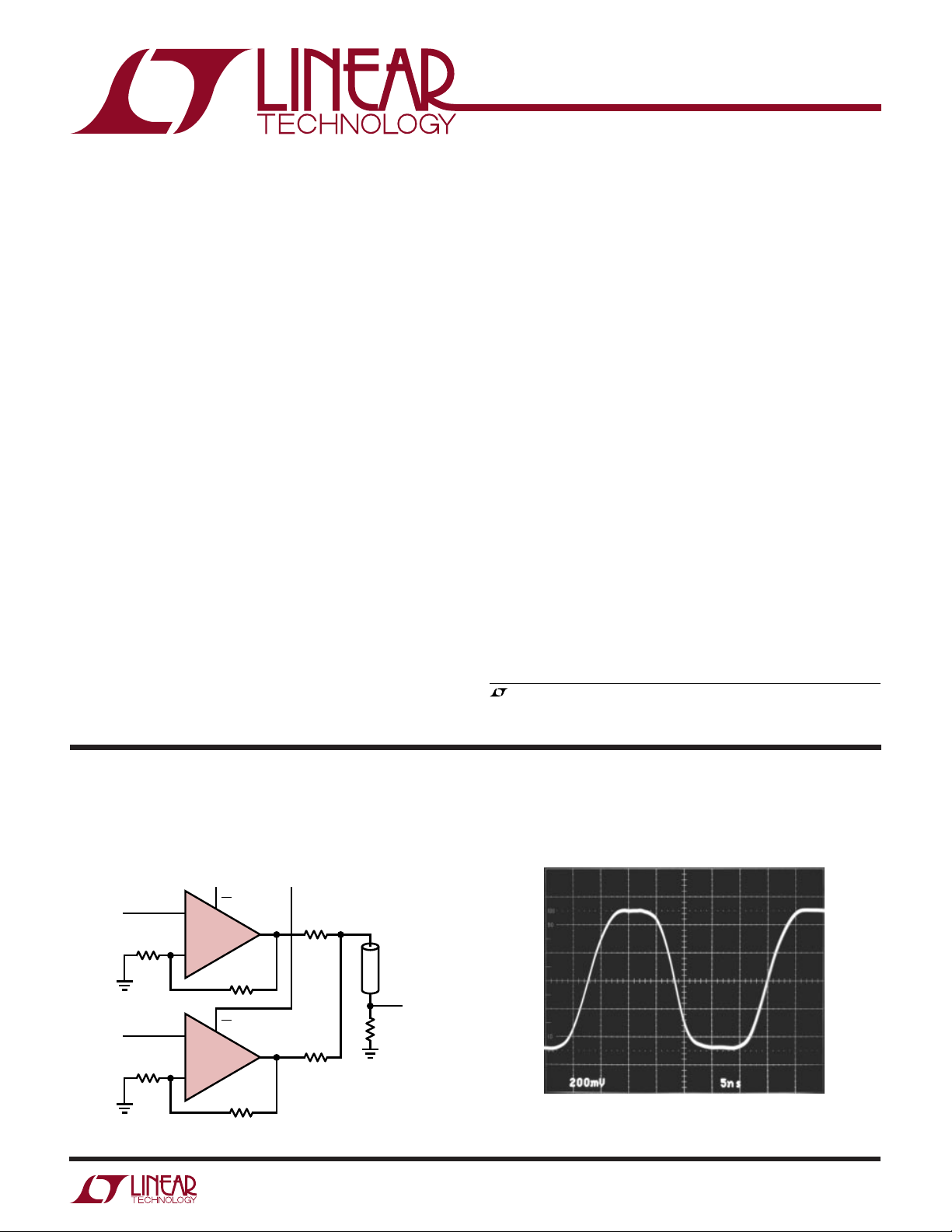
TYPICAL APPLICATIO
CHANNEL
A
SELECT
V
IN A
R
G
1.6k
V
IN B
R
G
1.6k
EN A
+
1/2 LT1259
–
EN B
+
1/2 LT1259
–
R
1.6k
R
1.6k
B
F
F
U
75Ω
75Ω
LT1259/60 • TA01
75Ω
CABLE
75Ω
The LT1259/LT1260 amplifiers are manufactured on
Linear Technology’s proprietary complementary bipolar
process.
, LTC and LT are registered trademarks of Linear Technology Corporation.
Square Wave Response2-Input Video MUX Cable Driver
V
OUT
CABLE OUTPUT
RL = 150Ω
f = 30MHz
LT1259/50 • TA02
1
Page 2
LT1259/LT1260
WWWU
ABSOLUTE AXI U RATI GS
Supply Voltage ..................................................... ±18V
Input Current ..................................................... ±15mA
Output Short-Circuit Duration (Note 1).........Continuous
Specified Temperature Range (Note 2)....... 0°C to 70°C
UU
W
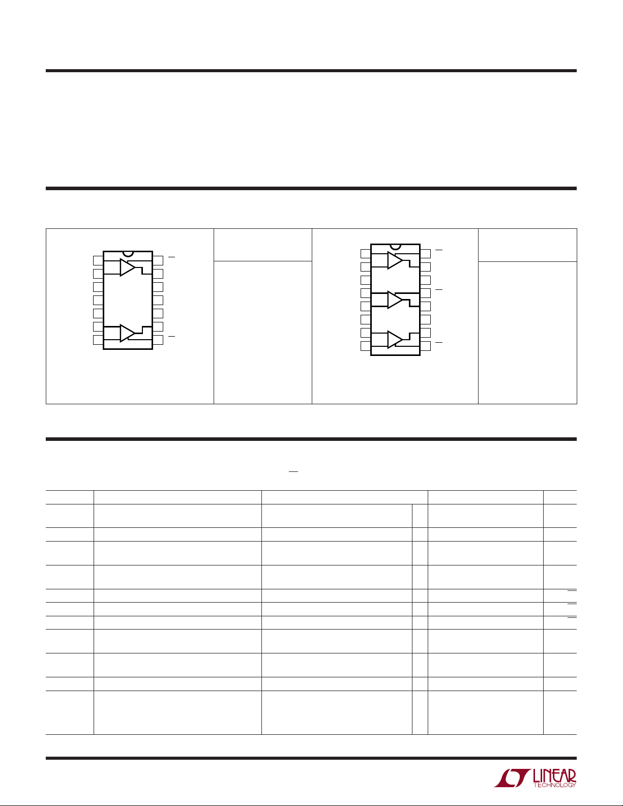
PACKAGE/ORDER I FOR ATIO
TOP VIEW
1
–IN A
2
+IN A
3
GND
4
GND
5
GND
6
+IN B
7
–IN B
N PACKAGE
14-LEAD PLASTIC DIP
T
= 150°C, θJA = 70°C/W (N)
JMAX
T
= 150°C, θJA = 110°C/W (S)
JMAX
EN A
A
B
14
OUT A
13
+
V
12
GND
11
–
V
10
OUT B
9
EN B
8
S PACKAGE
14-LEAD PLASTIC SOIC
ORDER PART
NUMBER
LT1259CN
LT1259CS
LT1259IN
LT1259IS
Operating Temperature Range ............... –40°C to 85°C
Storage Temperature Range ................ –65°C to 150°C
Junction Temperature (Note 4)............................ 150°C
Lead Temperature (Soldering, 10 sec).................. 300°C
TOP VIEW
1
–IN R
2
+IN R
3
GND
4
–IN G
5
+IN G
6
GND
7
+IN B
8
–IN B
N PACKAGE
16-LEAD PLASTIC DIP
T
= 150°C, θJA = 70°C/W (N)
JMAX
= 150°C, θJA = 100°C/W (S)
T
JMAX
EN R
R
G
B
16
OUT R
15
+
V
14
EN G
13
OUT G
12
–
V
11
OUT B
10
EN B
9
S PACKAGE
16-LEAD PLASTIC SOIC
ORDER PART
NUMBER
LT1260CN
LT1260CS
LT1260IN
LT1260IS
Consult factory for Military grade parts.
ELECTRICAL CHARACTERISTICS
0°C ≤ TA ≤ 70°C, each amplifier VCM = 0V, ±5V ≤ VS ≤ ±15V, EN pins = 0V, pulse tested, unless otherwise noted.
SYMBOL PARAMETER CONDITIONS MIN TYP MAX UNITS
V
I
I
e
+i
–i
R
C
C
V
IN
IN
n
OS
+
–
n
n
IN
IN
OUT
IN
Input Offset Voltage TA = 25°C212mV
● 16 mV
Input Offset Voltage Drift ● 30 µV/°C
Noninverting Input Current TA = 25°C 0.5 3 µA
● 6 µA
Inverting Input Current TA = 25°C2090µA
● 120 µA
Input Noise Voltage Density f = 1kHz, RF = 1k, RG = 10Ω, RS = 0Ω 3.6 nV/√Hz
Noninverting Input Noise Current Density f = 1kHz 1.3 pA/√Hz
Inverting Input Noise Current Density f = 1kHz 45 pA/√Hz
Input Resistance VIN = ±13V, VS = ±15V ● 217 MΩ
= ±3V, VS = ±5V ● 225 MΩ
V
IN
Input Capacitance Enabled 2 pF
Disabled 4 pF
Output Capacitance Disabled 4.4 pF
Input Voltage Range VS = ±15V, TA = 25°C ±13 ±13.5 V
● ±12 V
VS = ±5V, TA = 25°C ±3 ±3.5 V
● ±2V
2
Page 3
LT1259/LT1260
LECTRICAL C CHARA TERIST
E
0°C ≤ TA ≤ 70°C, each amplifier VCM = 0V, ±5V ≤ VS ≤ ±15V, EN pins = 0V, pulse tested, unless otherwise noted.
SYMBOL PARAMETER CONDITIONS MIN TYP MAX UNITS
V
OUT
CMRR Common-Mode Rejection Ratio VS = ±15V, VCM = ±13V, TA = 25°C5569 dB
PSRR Power Supply Rejection Ratio VS = ±2V to ±15V, EN Pins at V–, TA = 25°C6080 dB
A
V
R
OL
I
OUT
I
S
SR Slew Rate (Note 6) TA = 25°C 900 1600 V/µs
t
ON
t
OFF
tr, t
f
t
S
Maximum Output Voltage Swing VS = ±15V, RL = 1k ● ±12.0 ±14.0 V
Inverting Input Current VS = ±15V, VCM = ±13V, TA = 25°C 3.5 10 µA/V
Common-Mode Rejection V
Noninverting Input Current VS = ±3V to ±15V, EN Pins at V–, TA = 25°C1565nA/V
Power Supply Rejection VS = ±3V to ±15V, EN Pins at V
Inverting Input Current VS = ±2V to ±15V, EN Pins at V–, TA = 25°C 0.1 5 µA/V
Power Supply Rejection V
Large-Signal Voltage Gain VS = ±15V, V
Transresistance, ∆V
OUT
/∆I
–
IN
Maximum Output Current RL = 0Ω, TA = 25°C3060mA
Supply Current per Amplifier VS = ±15V, V
(Note 5)
Disable Supply Current per Amplifier VS = ±15V, EN Pin Voltage = 14.5V, RL = 150Ω ● 3 16.7 µA
Enable Pin Current VS = ±15V, EN Pin Voltage = 0V, TA = 25°C 60 200 µA
Turn-On Delay Time (Note 7) AV = 10, TA = 25°C 100 400 ns
Turn-Off Delay Time (Note 7) AV = 10, TA = 25°C 40 150 ns
Small-Signal Rise and Fall Time VS = ±12V, RF = RG = 1.5k, RL = 150Ω 4.2 ns
Propagation Delay VS = ±12V, RF = RG = 1.5k, RL = 150Ω 4.7 ns
Small-Signal Overshoot VS = ±12V, RF = RG = 1.5k, RL = 150Ω 5%
Settling Time 0.1%, V
Differential Gain (Note 8) VS = ±12V, RF = RG = 1.5k, RL = 150Ω 0.016 %
Differential Phase (Note 8) VS = ±12V, RF = RG = 1.5k, RL = 150Ω 0.075 DEG
ICS
VS = ±5V, RL = 150Ω, TA = 25°C ±3.0 ±3.7 V
VS = ±15V, VCM = ±12V ● 55 dB
= ±5V, VCM = ±3V, TA = 25°C5263dB
V
S
= ±5V, VCM = ±2V ● 52 dB
V
S
= ±15V, VCM = ±12V ● 10 µA/V
S
= ±5V, VCM = ±3V, TA = 25°C 4.5 15 µA/V
V
S
VS = ±5V, VCM = ±2V ● 15 µA/V
= ±3V to ±15V, EN Pins at V
V
S
= ±3V to ±15V, EN Pins at V
S
= ±10V, RL = 1k ● 57 72 dB
= ±5V, V
V
S
VS = ±15V, V
VS = ±5V, V
VS = ±5V, V
= ±15V, Sink 1µA From EN Pin ● 1 2.7 µA
V
S
OUT
= ±2V, RL = 150Ω ● 57 69 dB
OUT
= ±10V, RL = 1k ● 120 300 kΩ
OUT
= ±2V, RL = 150Ω ● 100 200 kΩ
OUT
= 0V, TA = 25°C 5.0 7.5 mA
OUT
= 0V, TA = 25°C 4.5 6.7 mA
OUT
= 10V, RF = RG = 1.5k, RL = 1k 75 ns
OUT
–
–
–
● ±2.5 V
● 60 dB
● 75 nA/V
● 5 µA/V
● 7.9 mA
● 300 µA
–40°C ≤ TA ≤ 85°C, each amplifier VCM = 0V, ±5V ≤ VS ≤ ±15V, EN pins = 0V, pulse tested, unless otherwise noted.
SYMBOL PARAMETER CONDITIONS MIN TYP MAX UNITS
V
OS
+
I
IN
–
I
IN
R
IN
A
V
I
S
Input Offset Voltage ● 18 mV
Noninverting Input Current ● 7 µA
Inverting Input Current ● 130 µA
Input Resistance VIN = ±3V, VS = ±5V ● 1MΩ
Large-Signal Gain ● 55 dB
Disable Supply Current per Amplifier VS = ±15V, EN Pin Voltage = 14.5V, RL = 150Ω ● 19 µA
Enable Pin Current VS = ±15V, EN Pin Voltage = 0V ● 350 µA
3
Page 4

LT1259/LT1260
ELECTRICAL CHARACTERISTICS
T
he ● denotes specifications which apply over the specified operating
temperature range.
Note 1: A heat sink may be required depending on the power supply
voltage and how many amplifiers have their outputs short circuited.
Note 2: Commercial grade parts are designed to operate over the
temperature range of –40°C to 85°C but are neither tested nor guaranteed
beyond 0°C to 70°C. Industrial grade parts specified and tested over
–40°C to 85°C are available on special request. Consult factory.
Note 3: Ground pins are not internally connected. For best
performance, connect to ground.
Note 4: T
power dissipation P
is calculated from the ambient temperature TA and the
J
according to the following formulas:
D
LT1259CN/LT1259IN: TJ = TA + (PD • 70°C/W)
LT1259CS/LT1259IS: T
LT1260CNLT1260IN/: T
LT1260CS/LT1260IS: T
= TA + (PD • 110°C/W)
J
= TA + (PD • 70°C/W)
J
= TA + (PD • 100°C/W)
J
Note 5: The supply current of the LT1259/LT1260 has a negative
temperature coefficient. See Typical Performance Characteristics.
Note 6: Slew rate is measured at ±5V on a ±10V output signal while
operating on ±15V supplies with R
= 1k, RG = 110Ω and RL = 1k.
F
Note 7: Turn-on delay time is measured while operating on ±5V
supplies with R
= 1k, RG = 110Ω and RL = 150Ω. The tON is measured
F
from control input to appearance of 0.5V at the output, for V
Likewise, turn-off delay time is measured from control input to
appearance of 0.5V on the output for VIN = 0.1V.
Note 8: Differential gain and phase are measured using a Tektronix
TSG120YC/NTSC signal generator and a Tektronix 1780R Video
Measurement Set. The resolution of this equipment is 0.1% and 0.1°.
Six identical amplifier stages were cascaded giving an effective
resolution of 0.016% and 0.016°.
WU
TYPICAL AC PERFOR A CE
SMALL SIGNAL SMALL SIGNAL SMALL SIGNAL
(V) A
V
S
V
±12 2 150 1.5k 1.5k 130 53 0.1
±5 2 150 1.1k 1.1k 93 40 0
±12 10 150 1.1k 121 69 20 0.13
±5 10 150 825 90.9 61 16 0
RL (Ω)R
(Ω)R
F
(Ω) – 3dB BW (MHz) 0.1dB BW (MHz) PEAKING (dB)
G
= 0.1V.
IN
UW
TYPICAL PERFOR A CE CHARACTERISTICS
±12V Frequency Response, AV = 2
12
11
10
9
8
7
GAIN (dB)
6
5
4
3
2
1
GAIN
VS = ±12V
= 150Ω
R
L
= RG = 1.5k
R
F
PHASE
10 100
FREQUENCY (MHz)
LT1259/60 • TPC01
0
–20
–40
–60
–80
–100
–120
–140
–160
–180
–200
PHASE (DEG)
26
25
24
23
22
21
GAIN (dB)
20
19
18
17
16
±12V Frequency Response, AV = 10
VS = ±12V
R
= 150Ω
L
= 1.1k
R
F
R
= 121Ω
PHASE
GAIN
1
10 100
FREQUENCY (MHz)
G
LT1259/60 • TPC01
0
–20
–40
–60
–80
–100
–120
–140
–160
–180
–200
PHASE (DEG)
4
Page 5

UW
TYPICAL PERFOR A CE CHARACTERISTICS
LT1259/LT1260
±5V Frequency Response, AV = 2
12
11
10
9
8
7
GAIN (dB)
6
5
4
3
2
VS = ±5V
R
L
R
F
1
GAIN
= 150Ω
= RG = 1.1k
Total Harmonic Distortion
vs Frequency
0.1
VS = ±12V
R
= 400Ω
L
R
= RG = 1.5k
F
VO = 6V
RMS
0.01
VO = 1V
TOTAL HARMONIC DISTORTION (%)
0.001
10
100 10k
1k 100k
FREQUENCY (Hz)
PHASE
10 100
FREQUENCY (MHz)
RMS
LT1259/60 • TPC05
LT1259/60 • TPC03
–20
–30
–40
–50
DISTORTION (dBc)
–60
–70
±5V Frequency Response, AV = 10
0
–20
–40
–60
–80
–100
–120
–140
–160
–180
–200
PHASE (DEG)
26
25
24
23
22
21
GAIN (dB)
20
19
18
17
16
1
VS = ±5V
R
L
R
= 825Ω
F
R
G
2nd and 3rd Harmonic Distortion
vs Frequency
VS = ±12V
V
= 2V
O
P-P
AV = 10dB
R
= 100Ω
L
R
= 1.5k
F
2ND 3RD
1
10 100
FREQUENCY (MHz)
LT12359/60 • TPC06
GAIN
= 150Ω
= 90.9Ω
PHASE
10 100
FREQUENCY (MHz)
LT1259/60 • TPC04
Maximum Undistorted Output
vs Frequency
25
20
)
P-P
15
10
OUTPUT VOLTAGE (V
5
0
1
AV = 1 AV = 2
FREQUENCY (MHz)
0
–20
–40
–60
PHASE (DEG)
–80
–100
–120
–140
–160
–180
–200
VS = ±15V
= 1k
R
L
R
= 2k
F
AV = 10
10 100
LT12359/60 • TPC07
Power Supply Rejection
vs Frequency
80
70
60
50
40
30
20
POWER SUPPLY REJECTION (dB)
10
0
10k
POSITIVE
100k 1M 10M
FREQUENCY (Hz)
VS = ±15V
R
= 1OOΩ
L
R
= RG = 1k
F
NEGATIVE
LTC1259/60 • TPC08
100M
Spot Noise Voltage and Current
vs Frequency Output Impedance vs Frequency
100
VS = ±15V
10
1
OUTPUT IMPEDANCE (Ω)
0.1
10k
100k 10M
RF = RG = 2k
1M 100M
FREQUENCY (Hz)
SPOT NOISE (nV/√Hz OR pA/√Hz)
100
–i
n
10
e
n
+i
n
1
10
100 10k
1k 100k
FREQUENCY (Hz)
LT1259/60 • TPC09
LT1259/60 • TPC10
5
Page 6

LT1259/LT1260
TEMPERATURE (°C)
–50
OUTPUT SHORT-CIRCUIT CURRENT (mA)
60
70
150
LT1259/60 • TPC15
50
40
0
50
100
80
–25
25
75
125
UW
TYPICAL PERFOR A CE CHARACTERISTICS
Output Impedance in Shutdown
vs Frequency
100
10
1
OUTPUT IMPEDANCE (kΩ)
0.1
100k
1M 10M 100M
FREQUENCY (Hz)
Output Saturation Voltage
vs Temperature
+
V
RL = ∞
≤ ±18V
±2V ≤ V
–0.5
–1.0
S
VS = ±15
= 1
A
V
= 1.5k
R
F
LT1259/60 • TPC11
Maximum Capacitive Load
vs Feedback Resistor
1000
VS = ±5V VS = ±15V
100
LOAD CAPACITANCE (pF)
10
265431
FEEDBACK RESISTOR (kΩ)
Input Common-Mode Limit
vs Temperature
+
V
–0.5
–1.0
–1.5
–2.0
V+ = 2V TO 18V
AV = 2
= 150Ω
R
L
PEAKING ≤ 5dB
LT1259/60 • TPC12
Supply Current vs Supply Voltage
7
6
5
4
3
2
SUPPLY CURRENT (mA)
1
0
218
46810
0
SUPPLY VOLTAGE (±V)
–55°C
25°C
125°C
12
Output Short-Circuit Current
vs Junction Temperature
14 16
LT1259/60 • TPC13
1.0
0.5
OUTPUT SATURATION VOLTAGE (V)
–
V
–50
–25 0
50 100 125
25 75
TEMPERATURE (°C)
LT1259/60 • TPC14
Settling Time to 10mV
vs Output Step
10
8
6
4
2
0
–2
OUTPUT STEP (V)
–4
–6
–8
–10
0
NONINVERTING
INVERTING
100 300
200
SETTLING TIME (ns)
400
500
2.0
1.5
COMMON-MODE RANGE (V)
1.0
0.5
–
V
–50
–25
VS = ±12V
R
= 1.5k
F
700
600
800
LT1259/60 • TPC17
V– = –2V TO –18V
50
25
0
TEMPERATURE (°C)
100
LT1259/60 • TPC16
125
75
Small-Signal Rise Time
R
VS = ±15V
= 2
A
V
= RG = 1.6k
F
= 150Ω
R
L
LT1259/60 G19
6
Page 7

WW
SI PLIFIED SCHE ATIC
, each amplifier
LT1259/LT1260
+
V
+IN
EN
WUUU
APPLICATIO S I FOR ATIO
Feedback Resistor Selection
The small-signal bandwidth of the LT1259/ LT1260 are set
by the external feedback resistors and the internal junction
capacitors. As a result, the bandwidth is a function of the
supply voltage, the value of the feedback resistor, the
closed-loop gain and the load resistor. The LT1259/LT1260
have been optimized for ±5V supply operation and have a
– 3dB bandwidth of 90MHz. See resistor selection guide in
Typical AC Performance table.
Capacitance on the Inverting Input
Current feedback amplifiers require resistive feedback
from the output to the inverting input for stable operation.
Take care to minimize the stray capacitance between the
output and the inverting input. Capacitance on the inverting input to ground will cause peaking in the frequency
response (and overshoot in the transient response). See
the section on Demo Board Information.
Capacitive Loads
The LT1259/LT1260 can drive capacitive loads directly
when the proper value of feedback resistor is used. The
graph of Maximum Capacitive Load vs Feedback Resistor
should be used to select the appropriate value. The value
shown is for ≤5dB peaking when driving a 150Ω load at a
gain of 2. This is a worst case condition. The amplifier is
–IN
OUT
V
LT1259/60 • SS
–
more stable at higher gains. Alternatively, a small resistor
(10Ω to 20Ω) can be put in series with the output to isolate
the capacitive load from the amplifier output. This has the
advantage that the amplifier bandwidth is only reduced
when the capacitive load is present. The disadvantage is
that the gain is a function of the load resistance.
Power Supplies
The LT1259/LT1260 will operate from single or split
supplies from ±2V (4V total) to ±15V (30V total). It is not
necessary to use equal value split supplies, however the
offset voltage and inverting input bias current will change.
The offset voltage changes about 500µV per volt of
supply mismatch. The inverting bias current can change
as much as 5µA per volt of supply mismatch though
typically, the change is about 0.1µA per volt.
Slew Rate
The slew rate of a current feedback amplifier is not
independent of the amplifier gain configuration the way
slew rate is in a traditional op amp. This is because both the
input stage and the output stage have slew rate limitations.
In the inverting mode, and for higher gains in the noninverting mode, the signal amplitude between the input pins
is small and the overall slew rate is that of the output stage.
For gains less than ten in the noninverting mode, the
overall slew rate is limited by the input stage.
7
Page 8

LT1259/LT1260
WUUU
APPLICATIO S I FOR ATIO
The input slew rate of the LT1259/LT1260 is approximately 270V/µs and is set by internal currents and capaci-
tances. The output slew rate is set by the value of the
feedback resistors and internal capacitances. At a gain of
10 with at 1k feedback resistor and ±15V supplies, the
output slew rate is typically 1600V/µs. Larger feedback
resistors will reduce the slew rate as will lower supply
voltages, similar to the way the bandwidth is reduced.
The graph of Maximum Undistorted Output vs Frequency
relates the slew rate limitations to sinusoidal input for
various gains.
Large-Signal Transient Response, AV = 2
looks like a 4.4pF capacitor in parallel with a 75k resistor,
excluding feedback resistor effects. These amplifiers are
designed to operate with open drain logic: the EN pins have
internal pullups and the amplifiers draw zero current when
these pins are high. To activate an amplifier, its EN pin is
pulled to ground (or at least 2V below the positive supply).
The enable pin current is approximately 60µA when
activated. Input referred switching transients with no
input signal applied are only 35mV positive and 80mV
negative with RL = 100Ω.
Output Switching Transient
EN
OUTPUT
VS = ±15V
= RG = 1.6k
R
F
RL = 400Ω
LT1259/LT1260 • AI01
Large-Signal Transient Response, AV = 10
VS = ±15V
= 1k
R
F
RG = 110Ω
= 400Ω
R
L
LT1259/LT1260 • AI02
Enable/Disable
The LT1259/LT1260 amplifiers have a unique high impedance, zero supply current mode which is controlled by
independent EN pins. When disabled, an amplifier output
VS = ±5V
= 0V
V
IN
RF = RG = 1.6k
= 100Ω
R
L
LT1259/LT1260 • AI03
The enable/disable times are very fast when driven from
standard 5V logic. The amplifier enables in about 100ns
(50% point to 50% point) while operating on ±5V supplies. Likewise the disable time is approximately 40ns
(50% point to 50% point) or 75ns to 90% of the final
value. The output decay time is set by the output capacitance and load resistor.
Amplifier Enable Time, AV = 10
OUTPUT
EN
VS = ±5V
= 0.1V
V
IN
RF = 1k
= 110Ω
R
G
R
L
= 150Ω
LT1259/LT1260 • AI04
8
Page 9

WUUU
APPLICATIO S I FOR ATIO
LT1259/LT1260
Amplifier Disable Time, AV = 10
EN
OUTPUT
VS = ±5V
V
= 0.1V
IN
RF = 1k
= 110Ω
R
G
R
L
= 150Ω
LT1259/LT1260 • AI05
Differential Input Signal Swing
The differential input swing is limited to about ±6V by an
ESD protection device connected between the inputs. In
normal operation, the differential voltage between the
U
TYPICAL APPLICATIO S
Amplifier Enable/Disable Time, AV = 2
EN
OUTPUT
VS = ±5V
V
= 2VPP at 2MHz
IN
R
= RG = 1.6k
F
= 100Ω
R
L
LT1259/LT1260 • AI06
input pins is small, so this clamp has no effect. In the
disabled mode however, the differential swing can be the
same as the input swing, and the clamp voltage will set the
maximum allowable input voltage.
2-Input Video MUX Cable Driver
The application on the first page shows a low cost, 2input video MUX cable driver. The scope photo displays
the cable output of a 30MHz square wave driving 150Ω.
In this circuit the active amplifier is loaded by RF and R
G
of the disabled amplifier, but in this case it only causes a
1.2% gain error. The gain error can be eliminated by
2-Input Video MUX Switching Response
EN A
EN B
VS = ±5V
V
= V
IN A
= 2VPP at 2MHz
IN 2
R
= RG = 1.6k
F
R
= 100Ω
L
LT1259/LT1260 • TA03
configuring each amplifier as a unity-gain follower. The
switching time between channels is 100ns when both
EN A and EN B are driven.
2-Input RGB MUX Cable Driver Demonstration Board
A complete 2-input RGB MUX has been fabricated on PC
Demo Board #039A. The board incorporates two LT1260s
with outputs summed through 75Ω back termination
resistors as shown in the schematic. There are several
things to note about Demo Board #039A:
1. The feedback resistors of the disabled LT1260 load
the enabled amplifier and cause a small (1% to 2%)
gain error depending on the values of RF and RG.
Configure the amplifiers as unity-gain followers to
eliminate this error.
2. The feedback node has minimum trace length connecting RF and RG to minimize stray capacitance.
3. Ground plane is pulled away from RF and RG on both
sides of the board to minimize stray capacitance.
9
Page 10

LT1259/LT1260
FREQUENCY (MHz)
1
–100
ALL HOSTILE CROSSTALK (dB)
–80
–60
–40
–20
10 100
LT1259/60 • TA06
0
VS = ±12V
R
L
= 100Ω
R
F
= RG = 1.6k
R
S
= 10Ω
G
B
R
TYPICAL APPLICATIO S
U
4. Capacitors C1 and C6 are optional and only needed to
reduce overshoot when EN 1 or EN 2 are activated with
a long inductive ground wire.
5. The R, G and B amplifiers have slightly different
frequency responses due to different output trace
routing to RF (between pins 3 and 4). All amplifiers
have slightly less bandwidth in PCB #039 than when
measured alone as shown in the Typical AC Performance table.
6. Part-to-part variation can change the peaking by
±0.25dB.
RGB Demo Board Gain vs Frequency
4
VS = ±12V
= 150Ω
R
L
= RG = 1.6k
R
F
2
R
G
B
LT1259/60 • TA04
R, B
G
LT1259/60 • TA05
0
GAIN (dB)
–2
–4
–6
1
10 100
FREQUENCY (MHz)
RGB Demo Board Gain vs Frequency
4
VS = ±5V
R
= 150Ω
L
= RG = 1.1k
R
F
2
0
GAIN (dB)
–2
–4
–6
1
10 100
FREQUENCY (MHz)
RGB Demo Board All Hostile Crosstalk
P-DIP PC Board #039
EN1EN2
R1
G1
B1
R2
G2
B2
R10
R11
R2
R3
R4
R5
R8
R9
R1
R6
R7
R12
C1
C6
U1
R13
C2
R14
C3
R15
U2
C5
R16
C7
R17
C8
R18
(408) 432-1900
LT1260 RGB AMPLIFIER
DEMONSTRATION BOARD
C4
GNDV–V+
R
G
B
LT1259/60 • TA07
10
Page 11

PACKAGE DESCRIPTIO
0.300 – 0.325
(7.620 – 8.255)
0.009 – 0.015
(0.229 – 0.381)
+0.025
0.325
–0.015
+0.635
8.255
()
–0.381
*THESE DIMENSIONS DO NOT INCLUDE MOLD FLASH OR PROTRUSIONS.
MOLD FLASH OR PROTRUSIONS SHALL NOT EXCEED 0.010 INCH (0.254mm)
0.300 – 0.325
(7.620 – 8.255)
0.009 – 0.015
(0.229 – 0.381)
+0.025
0.325
–0.015
+0.635
8.255
()
–0.381
*THESE DIMENSIONS DO NOT INCLUDE MOLD FLASH OR PROTRUSIONS.
MOLD FLASH OR PROTRUSIONS SHALL NOT EXCEED 0.010 INCH (0.254mm)
0.010 – 0.020
(0.254 – 0.508)
0.008 – 0.010
(0.203 – 0.254)
*
DIMENSION DOES NOT INCLUDE MOLD FLASH. MOLD FLASH
SHALL NOT EXCEED 0.006" (0.152mm) PER SIDE
**
DIMENSION DOES NOT INCLUDE INTERLEAD FLASH. INTERLEAD
FLASH SHALL NOT EXCEED 0.010" (0.254mm) PER SIDE
0.010 – 0.020
(0.254 – 0.508)
0.008 – 0.010
(0.203 – 0.254)
*
DIMENSION DOES NOT INCLUDE MOLD FLASH. MOLD FLASH
SHALL NOT EXCEED 0.006" (0.152mm) PER SIDE
**
DIMENSION DOES NOT INCLUDE INTERLEAD FLASH. INTERLEAD
FLASH SHALL NOT EXCEED 0.010" (0.254mm) PER SIDE
× 45°
0.016 – 0.050
0.406 – 1.270
× 45°
0.016 – 0.050
0.406 – 1.270
0.015
(0.380)
MIN
0.015
(0.381)
MIN
0° – 8° TYP
(1.346 – 1.752)
0° – 8° TYP
0.130 ± 0.005
(3.302 ± 0.127)
0.125
(3.175)
MIN
0.130 ± 0.005
(3.302 ± 0.127)
0.125
(3.175)
MIN
0.053 – 0.069
(1.346 – 1.752)
0.014 – 0.019
(0.355 – 0.483)
0.053 – 0.069
0.014 – 0.019
(0.355 – 0.483)
U
Dimensions in inches (millimeters) unless otherwise noted.
N Package
14-Lead PDIP (Narrow 0.300)
(LTC DWG # 05-08-1510)
0.045 – 0.065
(1.143 – 1.651)
0.255 ± 0.015*
0.065
(6.477 ± 0.381)
(1.651)
TYP
0.005
(0.125)
MIN
0.100 ± 0.010
(2.540 ± 0.254)
0.018 ± 0.003
(0.457 ± 0.076)
N Package
16-Lead PDIP (Narrow 0.300)
(LTC DWG # 05-08-1510)
0.045 – 0.065
(1.143 – 1.651)
0.255 ± 0.015*
(6.477 ± 0.381)
0.065
(1.651)
TYP
0.005
(0.127)
MIN
0.100 ± 0.010
(2.540 ± 0.254)
0.018 ± 0.003
(0.457 ± 0.076)
S Package
14-Lead Plastic Small Outline (Narrow 0.150)
(LTC DWG # 05-08-1610)
0.004 – 0.010
(0.101 – 0.254)
0.228 – 0.244
0.050
(1.270)
TYP
(5.791 – 6.197)
S Package
16-Lead Plastic Small Outline (Narrow 0.150)
(LTC DWG # 05-08-1610)
0.004 – 0.010
(0.101 – 0.254)
0.228 – 0.244
0.050
(1.270)
TYP
(5.791 – 6.197)
14
16
1
13
14
1
2
16
1
14
15
3
2
LT1259/LT1260
0.770*
(19.558)
MAX
11
1213
31
2
14
15
2
3
0.337 – 0.344*
(8.560 – 8.738)
12
11
3
0.386 – 0.394*
(9.804 – 10.008)
13
4
4
13
12
5
4
0.770*
(19.558)
MAX
4
10
5
5
6
12
11
6
5
8
9
7
6
11
10
7
6
8910
7
N14 0695
910
8
7
N16 0695
0.150 – 0.157**
(3.810 – 3.988)
9
0.150 – 0.157**
(3.810 – 3.988)
8
S14 0695
S16 0695
Information furnished by Linear Technology Corporation is believed to be accurate and reliable.
However, no responsibility is assumed for its use. Linear Technology Corporation makes no representation that the interconnection of its circuits as described herein will not infringe on existing patent rights.
11
Page 12

LT1259/LT1260
TYPICAL APPLICATIO
U
Demonstration PC Board Schematic #039
EN 1
16
15
14
13
12
11
10
9
C6*
0.01µF
16
15
14
13
12
11
10
9
EN 2
C1*
0.01µF
R1 R2
1
–
R
+
LT1260
–
G
+
+
B
–
–
R
+
LT1260
–
G
+
+
B
–
R4
R10
2
3
4
5
6
7
8
R5
1
2
3
4
5
6
7
8
R11
R1
R3
G1
B1
R6
R7 R8
R2
R9
G2
B2
R12
+
V
C7
0.1µF
–
V
GND
R13
C2
0.1µF
C3
0.1µF
C4
4.7µF
75Ω
R14
75Ω
R15
75Ω
V
RED
OUT
V
GREEN
OUT
V
BLUE
OUT
+
+
C5
4.7µF
R16
75Ω
R17
75Ω
C8
0.1µF
R18
75Ω
LT1259/60 • TA08
*OPTIONAL
RELATED PARTS
PART NUMBER DESCRIPTION COMMENTS
LT1203/LT1205 150MHz Video Multiplexers 2:1 and Dual 2:1 MUXes with 25ns Switch Time
LT1204 4-Input Video MUX with Current Feedback Amplifier Cascadable Enable 64:1 Multiplexing
LT1227 140MHz Current Feedback Amplifier 1100V/µs Slew Rate, Shutdown Mode
LT1252/LT1253/LT1254 Low Cost Video Amplifiers Single, Dual and Quad Current Feedback Amplifiers
125960fas, sn125960 LT/TP 1197 REV A 4K • PRINTED IN USA
LINEAR TECHNOLOGY CORPORATION 1993
12
Linear Technology Corporation
1630 McCarthy Blvd., Milpitas, CA 95035-7417 ● (408) 432-1900
FAX: (408) 434-0507
●
TELEX: 499-3977 ● www.linear-tech.com
 Loading...