

Page 1
FEATURES
LT1249
Power Factor Controller
U
DESCRIPTIO
■
Standard 8-Pin Packages
■
High Power Factor Over Wide Load Range
with Line Current Averaging
■
International Operation Without Switches
■
Instantaneous Overvoltage Protection
■
Minimal Line Current Dead Zone
■
Typical 250µA Start-Up Supply Current
■
Rejects Line Switching Noise
■
Synchronization Capability
■
Low Quiescent Current: 9mA
■
Fast 1.5A Peak Current Gate Driver
U
APPLICATIO S
■
Universal Power Factor Corrected Power Supplies
■
Preregulators up to 1500W
, LTC and LT are registered trademarks of Linear Technology Corporation.
The 8-pin LT®1249 provides active power factor correction for universal offline power systems with very few
external parts. By using fixed high frequency PWM current
averaging without the need for slope compensation, the
LT1249 achieves far lower line current distortion, with a
smaller magnetic element than systems that use either peak
current detection or zero current switching approach, in
both continuous and discontinuous modes of operation.
The LT1249 uses a multiplier containing a square gain
function from the voltage amplifier to reduce the AC gain
at light output load and thus maintains low line current
distortion and high system stability. The LT1249 also
provides filtering capability to reject line switching noise
which can cause instability when fed into the multiplier.
Line current dead zone is minimized with low bias voltage
at the current input to the multiplier.
The LT1249 provides many protection features including
peak current limiting and overvoltage protection. The
switching frequency is internally set at 100kHz.
While the LT1249 simplifies PFC design with minimal
parts count, the LT1248 provides flexibilities in switching
frequency, overvoltage and current limit.
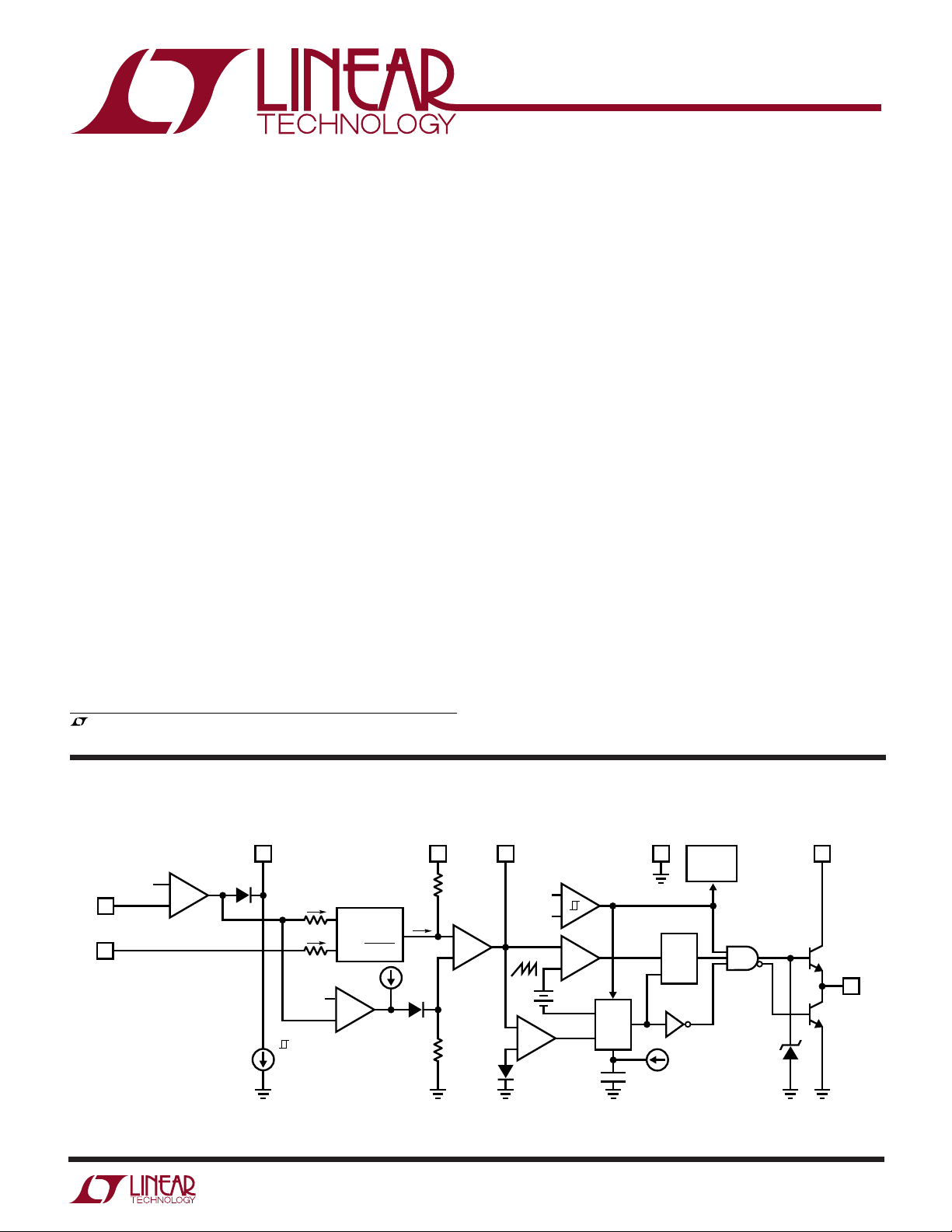
BLOCK DIAGRA
VA
OUT
5
+
7.5V
V
SENSE
6
I
AC
4
EA
–
W
44µA
22µA
MOUT
250µA MAX
+
CA
–
= 1/3k
g
m
CA
OUT
16V/10V
+
–
GND
1
7.5V
V
REF
+
V
CC
–
–
+
+
0.7V
SYNC
RUN
OSC
R
S
20µA
35pF
RUN
Q
16V
M
OUT
32
R
4k
I
A
MULTIPLIER
32k
I
IM =
B
1V
200µA
+
M1
–
I
M
2
I
I
A
B
2
15µA
4k
V
CC
7
GTDR
8
1249 BD
1
Page 2
LT1249
WW
W
U
ABSOLUTE MAXIMUM RATINGS
Supply Voltage ....................................................... 27V
GTDR Current Continuous ..................................... 0.5A
GTDR Output Energy (Per Cycle) ............................. 5µJ
IAC Input Current ................................................. 20mA
V
M
Operating Junction Temperature Range
Thermal Resistance (Junction-to-Ambient)
Storage Temperature Range ..................–65°C to 150°C
Lead Temperature (Soldering, 10 sec)................. 300°C
ELECTRICAL CHARACTERISTICS
range, otherwise specifications are at T
VA
Input Voltage ............................................ V
SENSE
Input Current.............................................. ±5mA
OUT
LT1249C................................................ 0°C to 100°C
LT1249I ........................................... –40°C to 125°C
N8 Package ................................................ 100°C/W
S8 Package................................................. 120°C/W
The ● denotes specifications which apply over the operating temperature
= 25°C. Maximum operating voltage (V
= 5V, no load on any outputs, unless otherwise noted.
OUT
A
MAX
U
W
PACKAGE/ORDER INFORMATION
ORDER PART
TOP VIEW
GND
1
CA
2
OUT
M
3
OUT
I
4
AC
N8 PACKAGE
8-LEAD PDIP
S8 PACKAGE
8-LEAD PLASTIC SO
T
= 125°C, θJA = 100°C/W (N8)
JMAX
T
= 125°C, θJA = 120°C/W (S8)
JMAX
Consult factory for Military grade parts.
) = 25V, VCC = 18V, I
MAX
GTDR
8
V
7
CC
V
6
SENSE
VA
5
OUT
= 100µA, CA
AC
NUMBER
LT1249CN8
LT1249IN8
LT1249CS8
LT1249IS8
S8 PART
MARKING
1249
1249I
= 3.5V,
OUT
U
PARAMETER CONDITIONS MIN TYP MAX UNITS
Overall
Supply Current (VCC in Undervoltage Lockout) VCC = Lockout Voltage – 0.2V ● 0.25 0.45 mA
Supply Current, On 11.5V ≤ VCC ≤ V
VCC Turn-On Threshold ● 15.5 16.5 17.5 V
VCC Turn-Off Threshold ● 9.5 10.5 11.5 V
Voltage Amplifier
V
Bias Current V
SENSE
Voltage Amp Gain 70 100 dB
Voltage Amp Unity-Gain Bandwidth 1.5 MHz
Voltage Amp Output High 0 ≤ Source Current ≤ 50µA ● 10 12 V
Voltage Amp Output Low 0 ≤ Sink Current ≤ 5µA ● 0.1 0.4 V
Voltage Amp Source Current ● 130 260 450 µA
Voltage Amp Sink Current Threshold Linear Operation, 2V < VA
Voltage Amp Sink Current Hysteresis 2V < VA
Current Amplifier
Current Amp Offset Voltage ● ±2 ±15 mV
Current Amp Transconductance ∆I
Current Amp Voltage Gain 2.5V ≤ V
Current Amp Source Current V
Current Amp Sink Current V
Current Amp Output High 7.4 8.1 V
Current Amp Output Low 1.2 2 V
= 0V to 7V ● –25 –250 nA
SENSE
OUT
= ±40µA ● 150 320 550 µmho
CAOUT
CAOUT
= 1V, IM = 0µV 100 145 220 µA
MOUT
= –0.3V, IM = 0µA 67 95 125 µA
MOUT
, CA
MAX
< 10V ● 14 22.5 30 µA
≤ 7.5V 500 1000 V/V
= 1V ● 812 mA
OUT
< 10V ● 33 44 57 µA
OUT
2
Page 3
LT1249
ELECTRICAL CHARACTERISTICS
range, otherwise specifications are at T
VA
= 5V, no load on any outputs, unless otherwise noted.
OUT
= 25°C. Maximum operating voltage (V
A
The ● denotes specifications which apply over the operating temperature
) = 25V, VCC = 18V, I
MAX
= 100µA, CA
AC
OUT
= 3.5V,
PARAMETER CONDITIONS MIN TYP MAX UNITS
Reference
Reference Output Voltage TA = 25°C, Measured at V
Pin 7.39 7.5 7.6 V
SENSE
Reference Output Voltage Worst Case All Line, Temperature ● 7.32 7.5 7.68 V
Reference Output Voltage Line Regulation V
LOCKOUT
< VCC < V
MAX
● –20 5 20 mV
Multiplier
Multiplier Output Current IAC = 100µA, VA
= 5V 35 µA
OUT
Multiplier Output Current Offset RAC = 1M from IAC to GND ● –0.05 –0.5 µA
Multiplier Max Output Current (I
Multiplier Max Output Voltage (I
)I
M(MAX)
• R
M(MAX)
)IAC = 450µA, VA
MOUT
= 450µA, VA
AC
= 7V (Note 2) ● – 375 –250 –150 µA
OUT
= 7V (Note 2) ● –1.25 –1.1 –0.96 V
OUT
Multiplier Gain Constant (Note 3) 0.035 V
IAC Input Resistance IAC from 50µA to 1mA 15 32 50 kΩ
Oscillator
Oscillator Frequency ● 75 100 125 kHz
Control Pin (CA
Synchronization Frequency Range Synchronizing Pulse Low ≤ 0.35V on CA
) Threshold Duty Cycle = 0 ● 1.3 1.8 2.3 V
OUT
OUT
● 127 160 kHz
Gate Driver
Max GTDR Output Voltage 0mA Load, 18V < V
GTDR Output High – 200mA Load, 11.5V ≤ VCC ≤ 15V ● V
CC
< V
(Note 4) ● 12 15 17.5 V
MAX
– 3.0 V
CC
GTDR Output Low (Device Unpowered) VCC = 0V, 50mA Load (Sinking) ● 0.9 1.5 V
GTDR Output Low (Device Active) 200mA Load (Sinking) ● 0.5 1 V
Peak GTDR Current 10nF from GTDR to GND 2 A
GTDR Rise and Fall Time 1nF from GTDR to GND 25 ns
GTDR Max Duty Cycle 90 96 %
–2
Note 1: Absolute Maximum Ratings are those values beyond which the life
Note 3: Multiplier Gain Constant: K =
of a device may be impaired.
Note 2: Current amplifier is in linear mode with 0V input common mode.
W
U
Note 4: Maximum GTDR output voltage is internally clamped for higher
voltages.
V
CC
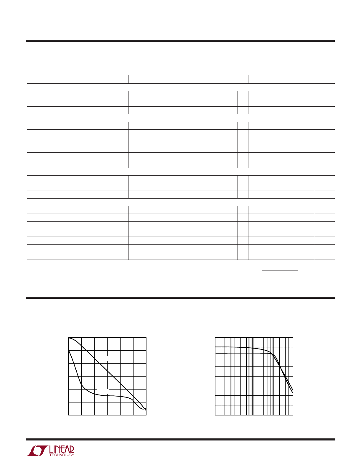
TYPICAL PERFORMANCE CHARACTERISTICS
Voltage Amplifier Open-Loop
Gain and Phase
100
80
60
40
GAIN (dB)
20
0
–20
10
100
GAIN
PHASE
1k 10k 100k
FREQUENCY (Hz)
1M 10M
1249 G01
0
–20
–40
–60
–80
–100
–120
PHASE (DEG)
400
350
300
250
200
150
100
TRANSCONDUCTANCE (µmho)
50
Transconductance of
Current Amplifier
θ
g
m
0
1k
100k10k
FREQUENCY (Hz)
IAC (VA
1M
I
OUT
M
– 1.5)
1249 G02
10M
2
20
0
–20
–40
–60
–80
–100
–120
–140
PHASE (DEG)
3
Page 4
LT1249
TEMPERATURE (°C)
–75
FREQUENCY (kHz)
75
1249 G10
–25 25 125
140
130
120
110
100
90
80
70
–50 0 50 100
W
U
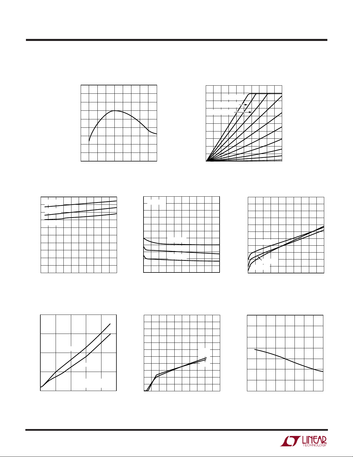
TYPICAL PERFORMANCE CHARACTERISTICS
Reference Voltage vs
Temperature
7.536
7.524
7.512
7.500
7.488
7.476
7.464
REFERENCE VOLTAGE (V)
7.452
7.440
7.428
–50 150
–75
–25
JUNCTION TEMPERATURE (°C)
0 25 50 100
75
125
1249 G03
Multiplier Current
300
150
(µA)
M
I
0
0
VA
500
= 5V
OUT
VA
= 4.5V
OUT
VA
= 4V
OUT
VA
= 3.5V
OUT
VA
= 3V
OUT
VA
= 2.5V
OUT
VA
= 2V
OUT
VA
= 6.5V
OUT
VA
= 6V
OUT
VA
= 5.5V
OUT
250
IAC (µA)
1249 G04
SUPPLY CURRENT (mA)
400
300
200
TIME (ns)
100
Supply Current vs Supply Voltage
10
TJ = –55°C
9
TJ = 25°C
8
7
TJ = 125°C
6
5
4
3
2
1
0
1412 16 20 24 28
10
SUPPLY VOLTAGE (V)
22
18
26
GTDR Rise and Fall Time
FALL TIME
RISE TIME
NOTE: GTDR SLEWS
0
0
10
BETWEEN 1V AND 16V
20 30 40
LOAD CAPACITANCE (nF)
1249 G05
1249 G08
GTDR Source Current
18.5
VCC = 18V
18.0
17.5
17.0
16.5
16.0
15.5
15.0
GTDR VOLTAGE (V)
14.5
14.0
13.5
13.0
30
0
TJ = 125°C
TJ = 25°C
TJ = –55°C
–120 –180 –240
–60
SOURCE CURRENT (mA)
–300
1249 G06
GTDR Sink Current
1.1
1.0
0.9
0.8
0.7
0.6
0.5
TA = –55°C
0.4
GTDR VOLTAGE (V)
0.3
0.2
0.1
0
TA = 125°C
0
TA = 25°C
60
120 180 240
SINK CURRENT (mA)
300
1249 G07
Start-Up Supply Current vs
Supply Voltage Switching Frequency
550
500
450
400
350
300
250
200
150
SUPPLY CURRENT (µA)
100
50
50
0
0
4
2610
SUPPLY VOLTAGE (V)
81216
–55°C
25°C
125°C
14 18
20
1249 G09
4
Page 5

W
TEMPERATURE (°C)
–50
TRANSCONDUCTANCE (µmho)
100
1249 G13
050
400
350
300
250
200
150
100
50
0
–25 25 75 125
U
TYPICAL PERFORMANCE CHARACTERISTICS
LT1249
Synchronization Threshold
at CA
1.0
0.9
0.8
0.7
0.6
0.5
0.4
0.3
0.2
SYNCHRONIZATION THRESHOLD (V)
0.1
OUT
0
–25 25 125–50 0 50
TEMPERATURE (°C)
75
100
Voltage Amp Sink Current Limits
(Threshold)
60
50
40
30
CURRENT (µA)
20
10
0
–75
NOTE: THESE SINK CURRENT THRESHOLDS ARE
FOR OVERVOLTAGE PROTECTION FUNCTION.
UP THRESHOLD
DOWN THRESHOLD
–25–50 250 50 10075125
TEMPERATURE (°C)
1249 G11
1249 G14
M
Pin Characteristics
OUT
1.2
1.0
0.8
0.6
0.4
0.2
0
CURRENT (mA)
–0.2
OUT
M
–0.4
–0.6
–0.8
–1.0
–2.4
125°C
25°C
–50°C
–1.2
M
OUT
0
VOLTAGE (V)
1.2
Maximum Multiplier Output
Voltage (I
–1.30
–1.25
–1.20
(V)
–1.15
MOUT
–1.10
× R
–1.05
M(MAX)
I
–1.00
–0.95
–0.90
–75 –25–50 250 50 10075125
• R
M(MAX)
TEMPERATURE (°C)
MOUT
)
2.4
1249 G12
1249 G15
Transconductance of Current
Amplifier Over Temperature
Maximum Duty Cycle
100
99
98
97
96
95
94
DUTY CYCLE (%)
93
92
91
90
–25 25 125–50 0 50
TEMPERATURE (°C)
75
100
1249 G16
UUU
PIN FUNCTIONS
GND (Pin 1): Ground.
CA
that senses and forces the line current to follow the
reference signal that comes from the multiplier by commanding the pulse width modulator. When CA
the modulator has zero duty cycle.
M
through the 4k resistor R
across R
and it is limited to 1.1V. The noninverting input of the
current amplifier is also tied to R
(Pin 2): This is the output of the current amplifier
OUT
OUT
(Pin 3): The multiplier current goes out of this pin
OUT
. The voltage developed
MOUT
is the reference voltage of the current loop
MOUT
. In operation, M
MOUT
is low,
OUT
is normally at negative potential and only AC signals
appear at the noninverting input of the current amplifier.
I
(Pin 4): This is the AC line voltage sensing input to the
AC
multiplier. It is a current input that is biased at 2V to
minimize the crossover dead zone caused by low line
voltage. A 32k resistor is in series with the current input,
so that a small external capacitor can be used to filter out
the switching noise from the high impedance lines.
VA
(Pin 5): This is the output of the voltage error
OUT
amplifier. The output is clamped at 12V. When the output
goes below 1.5V, the multiplier output current is zero.
5
Page 6

LT1249
UUU
PIN FUNCTIONS
V
(Pin 6): This is the inverting input to the voltage
SENSE
amplifier.
VCC (Pin 7): This is the supply of the chip. The LT1249 has
a very fast gate driver required to fast charge high power
MOSFET gate capacitance. High current spikes occur
during charging. For good supply bypass, a 0.1µF ceramic
U
WUU
APPLICATIONS INFORMATION
Error Amplifier
The error amplifier has a 100dB DC gain and 1.5MHz unitygain frequency. It is internally clamped at 12V. The noninverting input is tied to the 7.5V reference.
Current Amplifier
The multiplier output current IM flows out of the M
through the 4k resistor R
and develops the reference
MOUT
signal to the current loop that is controlled by the current
amplifier. Current gain is the ratio of R
to line current
MOUT
sense resistor. The current amplifier is a transconductance
amplifier. Typical gm is 320µmho and gain is 60dB with no
load. The inverting input is internally tied to GND. The
noninverting input is tied to the multiplier output. The
output is internally clamped at 8V. Output resistance is
about 4M; DC loading should be avoided because it will
lower the gain and introduce offset voltage at the inputs
which becomes a false reference signal to the current loop
and can distort line current. Note that in the current
averaging operation, high gain at twice the line frequency
is necessary to minimize line current distortion. Because
CA
may need to swing 5V over one line cycle at high line
OUT
condition, 11mV will be present at the inputs of the current
amplifier if gain is rolled off to 450 at 120Hz (1nF in series
with 10k at CA
). At light load, when (IM)(R
OUT
MOUT
less than 100mV, lower gain will distort the current loop
reference signal and line current. If signal gain at the
100kHz switching frequency is too high, the system
behaves more like a current mode system and can cause
subharmonic oscillation. Therefore, the current amplifier
should be compensated to have a gain of less than 15 at
100kHz and more than 300 at 120Hz.
pin
OUT
) can be
capacitor in parallel with a low ESR electrolytic capacitor,
56µF or higher is required in close proximity to IC GND.
GTDR (Pin 8): The MOSFET gate driver is a 1.5A fast totem
pole output. It is clamped at 15V. Capacitive loads like
MOSFET gates may cause overshoot. A gate series resistor of at least 5Ω will prevent the overshoot.
Multiplier
The multiplier is a current multiplier with high noise
immunity in a high power switching environment. The
current gain is:
IM = (IAC)(I
IEA = (VA
2
)/(200µA)2, and
EA
– 1.5V)/25k
OUT
With a square function, because of the lower gain at light
power load, system stability is maintained and line current
distortion caused by the AC ripple fed back to the error
amplifier is minimized. Note that switching ripple on the
high impedance lines could get into the multiplier from the
IAC pin and cause instability. The LT1249 provides an
internal 25k resistor in series with the low impedance
multiplier current input so that only a capacitor from the
IAC pin to GND is needed to filter out the noise. Maximum
multiplier output current is limited to 250µA. Figure 1
shows the multiplier transfer curves.
300
VA
500
VA
VA
VA
VA
VA
VA
OUT
OUT
OUT
OUT
OUT
OUT
OUT
OUT
= 5V
= 4.5V
= 4V
= 3.5V
= 3V
= 2.5V
= 2V
VA
= 6.5V
OUT
VA
= 6V
OUT
VA
= 5.5V
OUT
150
(µA)
M
I
0
0
Figure 1. Multiplier Current IM vs IAC and VA
250
IAC (µA)
1249 G04
6
Page 7

LT1249
U
WUU
APPLICATIONS INFORMATION
Line Current Limiting
Maximum voltage across R
1.1V. Therefore, line current limit is 1.1V divided by the
sense resistor RS. With a 0.2Ω sense resistor RS line
current limit is 5.5A. As a general rule, RS is chosen
according
IRV
()()( )
M MAX MOUT LINE MIN
R
S
where P
() ()
=
OUT(MAX)
1 414
KP
(. )
OUT MAX
is the maximum power output and K is
usually between 1.1 and 1.3 depending on efficiency and
resistor tolerance. When the output is overloaded and line
current reaches limit, output voltage V
line current constant. System stability is still maintained
by the current loop which is controlled by the current
amplifier. Further load current increase results in further
V
drop and clipping of the line current, which degrades
OUT
power factor.
Synchronization
The LT1249 can be externally synchronized in a frequency
range of 127kHz to 160kHz. Figure 2 shows the synchronizing circuit. Synchronizing occurs when CA
pulled below 0.5V with an external transistor and a Schottky
diode. The Schottky diode and the 10k pull-up resistor are
necessary for the required fast slewing back up to the
normal operating voltage on CA
turned off. Positive slewing on CA
than the oscillator ramp rate of 0.5V/µs.
The width of the synchronizing pulse should be under
60ns. The synchronizing pulses introduce an offset voltage on the current amplifier inputs, according to:
V
C
+
C
g
m
∆V
OS
ts fs I
()()
=
ts = pulse width
fs = pulse frequency
IC = CA
VC = CA
source current (≈ 150µA)
OUT
operating voltage (1.8V to 6.8V)
OUT
R2 = resistor for the midfrequency “zero” in the current loop
gm = current amplifier transconductance (≈ 320µmho)
is internally limited to
MOUT
()
will drop to keep
OUT
after the transistor is
OUT
should be faster
OUT
−
.05
R
2
OUT
pin is
With ts = 30ns, fs = 130kHz, VC = 3V and R2 = 10k, offset
voltage shift is ≈5mV. Note that this offset voltage will add
slight distortion to line current at light load.
CA
OUT
R2
10k
1nF
Figure 2. Synchronizing the LT1249
1N5712
2N2369
V
CC
R1
10k
80pF
2k
5V
0V
1249 F02
Overvoltage Protection
In Figure 3, R1 and R2 set the regulator output DC level:
V
V
OUT
OUT
= V
is 382V.
[(R1 + R2)/R2]. With R1 = 1M and R2 = 20k,
REF
Because of the slow loop response necessary for power
factor correction, output overshoot can occur with sudden
load removal or reduction. To protect the power components and output load, the LT1249 voltage error amplifier
senses the output voltage and quickly shuts off the current
switch when overvoltage occurs. When overshoot occurs
on V
because amplifier feedback keeps V
, the overcurrent from R1 will go through VA
OUT
locked at 7.5V.
SENSE
OUT
When this overcurrent reaches 44µA amplifier sinking
limit, the amplifier loses feedback and its output snaps low
to turn the multiplier off.
Overvoltage trip level: ∆V
V
OUT
R1
1M
R2
20k
0.047µF
C1
0.47µF
V
SENSE
–
+
V
REF
7.5V
Figure 3. Overvoltage Protection
= (44µA)(R1)
OUT
EA
MULTIPLIER
LT1249
R3
330k
VA
OUT
44µA
22µA
1249 F03
7
Page 8

LT1249
U
WUU
APPLICATIONS INFORMATION
The Figure 3 circuit therefore has 382V on V
overvoltage level = (V
hysteresis, V
then has to drop 22V to 404V before
OUT
+ 44V), or 426V. With a 22µA
OUT
feedback recovers and the switch turns back on.
M
is a high impedance current output. In the current
OUT
loop, offset line current is determined by multiplier offset
current and input offset voltage of the current amplifier.
A negative 4mV current amplifier VOS translates into
20mA line current and 5W input power for 250V line if
0.2Ω sense resistor is used. Under no load or when the
load power is less than this offset input power, V
slowly charge up to an overvoltage state because the
overvoltage comparator can only reduce multiplier output
current to zero. This does not guarantee zero output
current if the current amplifier has offset. To regulate V
under this condition, the amplifier M1 (see Block Diagram), becomes active in the current loop when VA
goes down to 1V. The M1 can put out up to 15µA to the 4k
resistor at the inverting input to cancel the current amplifier negative VOS and keep V
error to within 2V.
OUT
OUT
OUT
, and an
would
OUT
OUT
LINE
MAIN INDUCTOR
N
P
N
S
D2
ALL CAPACITORS ARE RATED 35V
Figure 4. Power Supply for LT1249
C2
1000pF
450V
D2
+
D1
C3
390µF
35V
R1
90k
1W
+
C1
2µF
+
+
C2
2µF
D3
+
MAIN INDUCTOR
R1
90k
1W
LINE
18V
C4
56µF
35V
D3D1
C3
390µF
V
CC
+
C4
56µF
1249 F04
V
CC
1249 F05
Undervoltage Lockout
The LT1249 turns on when VCC is higher than 16V and
remains on until VCC falls below 10V, whereupon the chip
enters the lockout state. In the lockout state, the LT1249
only draws 250µA, the oscillator is off, the V
and the
REF
GTDR pins remain low to keep the power MOSFET off.
Start-Up and Supply Voltage
The LT1249 draws only 250µA before the chip starts at
16V on VCC. To trickle start, a 90k resistor from the power
line to VCC supplies the trickle current and C4 holds the V
CC
up while switching starts (see Figure 4). Then the auxiliary
winding takes over and supplies the operating current.
Note that D3 and the large value C3, in both Figures 4 and
5, are only necessary for systems that have sudden large
load variation down to minimum load and/or very light
load conditions. Under these conditions, the loop may
exhibit a start/restart mode because switching remains off
long enough for C4 to discharge below 10V. The C3 will
hold VCC up until switching resumes. For less severe load
variations, D3 is replaced with a short and C3 is omitted.
The turns ratio between the primary winding and the
Figure 5. Power Supply for LT1249
auxiliary winding determines VCC according to: V
– 2V) = NP/NS. For 382V V
and 18V VCC, NP/NS ≈ 19.
OUT
OUT
/(V
CC
In Figure 5 a new technique for supply voltage eliminates
the need for an extra inductor winding. It uses capacitor
charge transfer to generate a constant current source
which feeds a Zener diode. Current to the Zener is equal to
(V
– VZ)(C)(f), where VZ is Zener voltage and f is
OUT
switching frequency. For V
= 382V, VZ = 18V, C =
OUT
1000pF and f = 100kHz, Zener current will be 36mA. This
is enough to operate the LT1249, including the FET gate
drive.
Output Capacitor
The peak-to-peak 120Hz output ripple is determined by:
V
= (2)(I
P-P
where I
LOAD
DC)(Z)
LOAD
DC: DC load current
Z: capacitor impedance at 120Hz
For 180µF at 300W load, I
DC = 300W/385V = 0.78A,
LOAD
8
Page 9

LT1249
U
WUU
APPLICATIONS INFORMATION
V
= (2)(0.78A)(7.4Ω) = 11.5V. If less ripple is desired,
P-P
higher capacitance should be used.
The selection of the output capacitor should also be based
on the operating ripple current through the capacitor.
The ripple current can be divided into three major compo-
nents. The first is at 120Hz whose RMS value is related to
the DC load current as follows:
I
≈ (0.71)(I
1RMS
The second component contains the PF switching frequency ripple current and its harmonics. Analysis of this
ripple is complicated because it is modulated with a 120Hz
signal. However, computer numerical integration and Fourier analysis approximate the RMS value reasonably close
to the bench measurements. The RMS value is about
0.82A at a typical condition of 120VAC, 200W load. This
ripple is line voltage dependent, and the worst case is at
low line.
I
= 0.82A at 120VAC, 200W
2RMS
The third component is the switching ripple from the load,
if the load is a switching regulator.
I
3RMS
≈ I
LOAD
DC
For United Chemicon KMH 400V capacitor series, ripple
current multiplier for currents at 100kHz is 1.43. The
equivalent 120Hz ripple current can then be found:
II
=
RMS RMS
()
1
For a typical system that runs at an average load of 200W
and 385V output:
I
DC = 0.52A
LOAD
I
≈ (0.71)(0.52A) = 0.37A
1RMS
I
≈ 0.82A at 120VAC
2RMS
I
≈ I
3RMS
IA
=
RMS
DC = 0.52A
LOAD
.
()
DC)
LOAD
2
II
+
2
+
2
RMS RMS
2
143 143..
082
.
143
.
3
+
22
AA
+
052
.
143
.
2
077
.
A
=037
The 120Hz ripple current rating at 105°C ambient is 0.95A
for the 180µF KMH 400V capacitor. The expected life of the
output capacitor may be calculated from the thermal
stress analysis:
CTKT
°+ +
()–()
LL
=
()()
O
10510∆∆
2
AMBTO
where
L = expected life time
LO = hours of load life at rated ripple current and rated
ambient temperature
∆TK = capacitor internal temperature rise at rated condi-
tion. ∆TK = (I2R)/(KA), where I is the rated current, R is
capacitor ESR, and KA is a volume constant.
T
= operating ambient temperature
AMB
∆TO = capacitor internal temperature rise at operating
condition
In our example, LO = 2000 hours and ∆TK = 10°C at rated
0.95A. ∆TO can then be calculated from:
∆∆T
I
=
O
095
22
RMS
.
A
()
T
K
=
077
095
.
A
().
CC
°= °
10 6 6
.
A
Assuming the operating ambient temperature is 60°C, the
approximate life time is:
CC C C
°+ ° °+ °
()–(.)
105 10 60 6 6
L
≈
()()
2000 2
O
≈
57,000 Hrs.
10
For longer life, capacitor with higher ripple current rating
or parallel capacitors should be used.
Protection Against Abnormal Current Surge
Conditions
The LT1249 has an upper limit on the allowed voltage
across the current sense resistor. The voltage into the
M
pin connected to this resistor must not exceed –6V
OUT
while the chip is running
The LT1249 gate drive will malfunction if the M
voltage exceeds – 6V while V
and –12V under any conditions.
pin
OUT
is powered, destroying the
CC
power FET. The 12V absolute limit is imposed by ESD
clamps on the M
pin. Large currents will flow at
OUT
9
Page 10

LT1249
U
WUU
APPLICATIONS INFORMATION
voltages above 8V and the 12V limit is only for surge
conditions.
In normal operation, the voltage into M
exceed 1.1V, but under surge conditions, the voltage
could temporarily go higher. To date, no field failures due
to surges have been reported for normal LT1249 configurations, but if the possibility exists for extremely large
current surges, please read the following discussion.
Offline switching power supplies can create large current
surges because of the high value storage capacitor used.
The surge can be the result of closing the line switch near
the peak of the AC line voltage, or because of a large
transient in the line itself. These surges are well known in
the power supply business, and are normally controlled
with a negative temperature coefficient thermistor in
series with the rectifier bridge. When power is switched
on, the thermistor is cold (high resistance) and surges are
limited. Current flow in the thermistor causes it to heat and
resistance drops to the point where overall efficiency loss
in the resistor is acceptable.
This basic protection mechanism can be partially defeated
if the power supply is switched off for a few seconds, then
turned back on. The thermistor has not had time to cool
significantly and if the subsequent turn-on catches the AC
line near its peak, the resulting surge is much higher than
normal. Even if this surge current generates a voltage
greater than 6V (but less than 12V) across the sense
does not
OUT
resistor, the standard LT1249 application will not be
affected because the chip is not yet powered. Problems are
only created if the VCC pin is powered from some external
housekeeping supply that remains powered when bridge
power is switched off.
A huge line voltage surge,
limits
, can also create a large current surge. The peak of
beyond the normal worst-case
the line voltage must significantly exceed the storage
capacitor voltage (typically 380V) for this to occur, so peak
line voltage would probably have to exceed 450V. Such
excessive surges might occur if a very large mains load
was suddenly removed, with a resulting line “kickback”. If
the surge results in voltage at the M
pin greater than
OUT
6V, it must also last more than 30µs (three switch cycles)
to cause FET problems.
External Clamp
The external clamp shown in Figure 6 will protect the
LT1249 M
surges (see above). Protection is provided for all V
pin against extremely large line current
OUT
CC
power methods. The 100Ω resistor and three diodes limit
the peak negative voltage into M
to less than 3V.
OUT
Current sense gain is attenuated by only 100Ω/4000Ω =
2.5%. Three diodes are used because the peak negative
voltage into M
in normal operation could go as high as
OUT
–1.1V and the diodes should not conduct more than a few
microamps under this condition.
10
THERMISTOR
+
BRIDGE
–
Figure 6. Protecting M
+
SURGE PATH
R
S
100Ω
M
OUT
LT1249
from Extremely High Current Surges
OUT
STORAGE
CAPACITOR
Page 11

PACKAGE DESCRIPTION
U
Dimensions in inches (millimeters) unless otherwise noted.
N8 Package
8-Lead PDIP (Narrow 0.300)
(LTC DWG # 05-08-1510)
0.400*
(10.160)
MAX
876
0.255 ± 0.015*
(6.477 ± 0.381)
5
LT1249
12
0.300 – 0.325
(7.620 – 8.255)
0.065
(1.651)
0.009 – 0.015
(0.229 – 0.381)
+0.035
0.325
–0.015
+0.889
8.255
()
–0.381
*THESE DIMENSIONS DO NOT INCLUDE MOLD FLASH OR PROTRUSIONS.
MOLD FLASH OR PROTRUSIONS SHALL NOT EXCEED 0.010 INCH (0.254mm)
TYP
0.045 – 0.065
(1.143 – 1.651)
0.100
(2.54)
BSC
S8 Package
8-Lead Plastic Small Outline (Narrow 0.150)
(LTC DWG # 05-08-1610)
8
3
0.189 – 0.197*
(4.801 – 5.004)
7
6
4
0.130 ± 0.005
(3.302 ± 0.127)
0.125
(3.175)
MIN
0.018 ± 0.003
(0.457 ± 0.076)
5
0.020
(0.508)
MIN
N8 1098
0.228 – 0.244
(5.791 – 6.197)
0.010 – 0.020
(0.254 – 0.508)
0.008 – 0.010
(0.203 – 0.254)
*
DIMENSION DOES NOT INCLUDE MOLD FLASH. MOLD FLASH
SHALL NOT EXCEED 0.006" (0.152mm) PER SIDE
**
DIMENSION DOES NOT INCLUDE INTERLEAD FLASH. INTERLEAD
FLASH SHALL NOT EXCEED 0.010" (0.254mm) PER SIDE
Information furnished by Linear Technology Corporation is believed to be accurate and reliable.
However, no responsibility is assumed for its use. Linear Technology Corporation makes no representation that the interconnection of its circuits as described herein will not infringe on existing patent rights.
× 45°
(1.346 – 1.752)
0°– 8° TYP
0.016 – 0.050
(0.406 – 1.270)
0.053 – 0.069
0.014 – 0.019
(0.355 – 0.483)
TYP
0.150 – 0.157**
(3.810 – 3.988)
1
3
2
4
0.004 – 0.010
(0.101 – 0.254)
0.050
(1.270)
BSC
SO8 1298
11
Page 12

LT1249
TYPICAL APPLICATION
U
90V
TO
270V
1M
4.7nF
100pF
+
–
–
+
SYNC
MURH860
GND
1
OSC
RUN
35pF
R
S
20µA
1M
20k
V
OUT
+
180µF
10Ω
†
V
CC
7
7.5V
V
REF
RUN
Q
GTDR
8
16V
**
1N5819
EMI
FILTER
6A
+
750µH*
–
IRF840
0.047µF
0.47µF
7.5V
6
V
SENSE
4
I
AC
330k
VA
OUT
5
+
EA
–
44µA
22µA
I
A
I
B
1V
32k
MULTIPLIER
IM =
+
M1
–
I
A
200µA
2
I
B
2
15µA
R
S
0.2Ω
1nF
10k
M
OUT
3
R
MOUT
4k
MAX
250µA
I
M
+
CA
–
g
= 1/3k
m
4k
CA
2
16V/10V
0.7V
+
–
OUT
V
CC
+
–
1. COILTRONICS CTX02-12236 (TYPE 52 CORE)
*
AIR MOVEMENT NEEDED AT POWER LEVEL GREATER THAN 250W.
2. COILTRONICS CTX02-12295 (MAGNETICS Kool Mµ
**
THIS SCHOTTKY DIODE IS TO CLAMP GTDR WHEN MOS SWITCH TURNS OFF.
PARASITIC INDUCTANCE AND GATE CAPACITANCE MAY TURN ON CHIP SUBSTRATE
DIODE AND CAUSE ERRATIC OPERATIONS IF GTDR IS NOT CLAMPED.
† SEE APPLICATIONS INFORMATION SECTION FOR CIRCUITRY TO SUPPLY POWER TO V
®
77930 CORE)
.
CC
1249 TA01
RELATED PARTS
PART NUMBER DESCRIPTION COMMENTS
LT1103 Off-Line Switching Regulator Universal Off-Line Inputs with Outputs to 100W
LT1248 Full Feature Average Current Mode Power Factor Controller Provides All Features in 16-Lead Package
LT1508 Power Factor and PWM Controller Simplified PFC Design
LT1509 Power Factor and PWM Controller Complete Solution for Universal Off-Line Switching Power Supplies
Kool Mµ is a registered trademark of Magnetics, Inc.
12
Linear Technology Corporation
1630 McCarthy Blvd., Milpitas, CA 95035-7417
(408) 432-1900 ● FAX: (408) 434-0507
●
www.linear-tech.com
1249fb LT/TP 0799 2K REV B • PRINTED IN USA
LINEAR TECHNOLOGY CORPORATION 1994
 Loading...