

Page 1
FEATURES
LT1248
Power Factor Controller
U
DESCRIPTIO
■
High Power Factor Over Wide Load Range
with Line Current Averaging
■
International Operation Without Switches
■
Instantaneous Overvoltage Protection
■
Minimal Line Current Dead Zone
■
Typical 250µA Start-Up Supply Current
■
Rejects Line Switching Noise
■
Synchronization Capability
■
Low Quiescent Current: 9mA
■
Fast 1.5A Peak Current Gate Driver
U
APPLICATIO S
■
Universal Power Factor Corrected Power Supplies
■
Preregulators Up To 1500W
The LT®1248 provides active power factor correction for
universal off-line power systems. By using fixed high
frequency PWM current averaging, without the need for
slope compensation, the LT1248 achieves far lower line
current distortion with a smaller magnetic element than
systems that use either peak-current detection or zero
current switching approaches in both continuous and
discontinuous modes of operation.
The LT1248 uses a multiplier containing a square gain
function from the voltage amplifier to reduce the AC gain
at light output load and thus maintains low line current
distortion and high system stability. The LT1248 also
provides filtering capability to reject line switching noise
which can cause instability when fed into the multiplier.
Line current dead zone is minimized with low bias voltage
at the current input to the multiplier.
The LT1248 provides many protection features including
peak current limiting and overvoltage protection, and can
be operated at frequencies as high as 300kHz.
, LTC and LT are registered trademarks of Linear Technology Corporation.
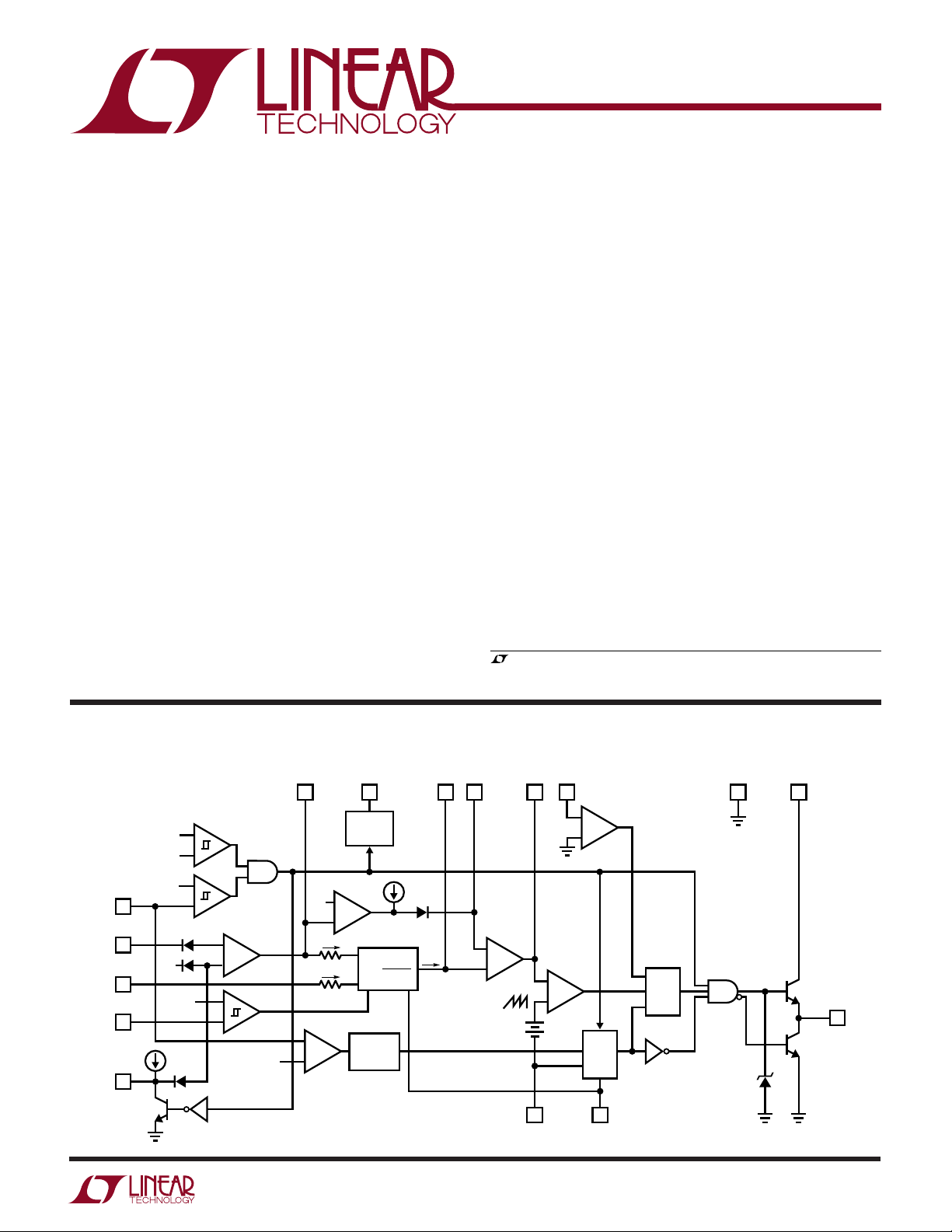
BLOCK DIAGRA
+
V
CC
2.6V/
2.2V
7.5V
7.9V
12µA
–
–
+
–
EA
+
+
–
5V
16V TO 10V
EN/SYNC
10
V
SENSE
11
I
AC
6
OVP
8
SS
13
W
–
CA
+
CA
PK
OUT
32
–
+
+
0.7V
–
SYNC
C
SET
LIM
GND
1
–
+
R
R
Q
S
RUN
OSC
1 6V
1214
R
SET
V
CC
15
16
GTDR
1248 BD
M
OUTISENSE
4
5
7µA
I
2
M
I
A
B
2
32k
+
M1
–
I
A
I
B
ONE SHOT
V
REF
9
7.5V
V
REF
IM =
200ns
RUN
I
200µA
VA
OUT
7
2.2V
–
+
1
Page 2
LT1248
A
W
O
LUTEXI TIS
S
A
WUW
ARB
U
G
PACKAGE
/
O
RDER I FOR ATIO
WU
U
(Note 1)
Supply Voltage ....................................................... 27V
GTDR Current Continuous ..................................... 0.5A
GTDR Output Energy(Per Cycle) .............................. 5µJ
IAC, R
V
SENSE
I
SENSE
SET
, PK
Input Current............................. 20mA
LIM
, EN/SYNC, OVP Input Voltage................... V
, M
Input Current.................................. ±5mA
OUT
MAX
Operating Junction Temperature Range
LT1248C................................................ 0°C to 100°C
LT1248I ........................................... –40°C to 125°C
GND
PK
CA
I
SENSE
M
VA
OVP
LIM
OUT
OUT
I
OUT
AC
Thermal Resistance (Junction-to-Ambient)
N Package .................................................. 100°C/W
S Package................................................... 120°C/W
Storage Temperature Range ..................–65°C to 150°C
16-LEAD NARROW PLASTIC SO
T
T
Lead Temperature (Soldering, 10 sec)................. 300°C
Consult factory for Military grade parts.
LECTRICAL C CHARA TERIST
E
ture range, otherwise specifications are at T
C
= 1nF to GND, I
SET
PARAMETER CONDITIONS MIN TYP MAX UNITS
Overall
Supply Current (VCC in Undervoltage Lockout) VCC = Lockout Voltage – 0.2V ● 0.25 0.45 mA
Supply Current (Inactive) EN/SYNC = 0V, VCC ≤ V
Supply Current, On 11.5V ≤ VCC ≤ V
VCC Turn-On Threshold (Undervoltage Lockout) ● 15.5 16.5 17.5 V
VCC Turn-Off Threshold ● 9.5 10.5 11.5 V
EN/SYNC Threshold, Rising ● 2.2 2.6 2.85 V
EN/SYNC Threshold Hysteresis 0.40 V
EN/SYNC Input Current EN/SYNC = 0V ● –5 –1 5 µA
Voltage Amplifier
Voltage Amp Offset Voltage VA
Input Bias Current V
Voltage Gain 70 100 dB
Voltage Amp Unity-Gain Bandwidth 3 MHz
Voltage Amp Output High (Internally Clamped) ● 11.3 13.3 V
Voltage Amp Output Low ● 1.1 2 V
Voltage Amp Short-Circuit Current VA
SS Current SS = 2.5V ● 51230 µA
Current Amplifier
Current Amp Offset Voltage ● ±1 ±4mV
I
Bias Current ● – 25 –250 nA
SENSE
Current Amp Voltage Gain 80 110 dB
Current Amp Unity-Gain Bandwidth 3 MHz
Current Amp Output High ● 7.2 8.5 V
Current Amp Output Low ● 1.1 2 V
= 100µA, I
AC
SENSE
= 0V, CA
ICS
= 25°C. Maximum operating voltage (V
A
OUT
The ● denotes specifications which apply over the full operating tempera-
= 3.5V, VA
3V ≤ EN/SYNC ≤ 7V –50 – 25 50 µA
OUT
SENSE
OUT
= 5V, OVP = 7.5V, no load on any outputs, unless otherwise noted.
OUT
MAX
, CA
MAX
OUT
= 3.5V ● –8 8 mV
= 0V to 7V ● – 25 –250 nA
= 0V ● 51430 mA
TOP VIEW
1
2
3
4
5
6
7
8
N PACKAGE
16-LEAD PDIP
S PACKAGE
= 125°C, θJA = 100°C/W (N)
JMAX
= 125°C, θJA = 120°C/W (S)
JMAX
) = 25V, VCC = 18V, R
MAX
= 1V ● 8.5 12.0 mA
GTDR
16
V
15
CC
C
14
SET
SS
13
R
12
SET
V
11
SENSE
EN/SYNC
10
V
9
REF
● 0.5 1.5 mA
ORDER PART
NUMBER
LT1248CN
LT1248IN
LT1248CS
LT1248IS
= 15k to GND,
SET
2
Page 3
LT1248
LECTRICAL C CHARA TERIST
E
ture range, otherwise specifications are at T
C
= 1nF to GND, I
SET
= 100µA, I
AC
SENSE
A
= 0V, CA
ICS
= 25°C. Maximum operating voltage (V
OUT
The ● denotes specifications which apply over the full operating tempera-
= 3.5V, VA
) = 25V, VCC = 18V, R
= 5V, OVP = 7.5V, no load on any outputs, unless otherwise noted.
OUT
MAX
= 15k to GND,
SET
PARAMETER CONDITIONS MIN TYP MAX UNITS
Current Amplifier
Current Amp Short-Circuit Current CA
Input Range, I
SENSE
, M
(Linear Operation) ● –0.3 1 V
OUT
= 0V ● 51430 mA
OUT
Reference
Reference Output Voltage I
V
Load Regulation –5mA < I
REF
V
Line Regulation 11.5V < VCC < V
REF
V
Short-Circuit Current V
REF
V
Worst Case Load, Line, Temperature ● 7.32 7.5 7.68 V
REF
= 0mA, TA = 25°C 7.39 7.50 7.60 V
REF
< 0mA 5 mV
REF
MAX
= 0V ● 12 28 50 mA
REF
● –20 5 20 mV
Current Limit
PK
Offset Voltage ● –15 15 mV
LIM
PK
Input Current PK
LIM
PK
to GTDR Propagation Delay PK
LIM
= –0.1V ● – 50 –100 µA
LIM
Falling from 50mV to –50mV 400 ns
LIM
Multiplier
Multiplier Output Current IAC = 100µA, R
= 15k 35 µA
SET
Multiplier Output Current Offset RAC = 1M from IAC to GND ● –0.05 –0.5 µA
Multiplier Maximum Output Current IAC = 450µA, R
= 15k, VA
SET
OUT
= 7V, M
= 0V ● –286 –260 – 235 µA
OUT
Multiplier Gain Constant (Note 2) 0.035 V
IAC Input Resistance IAC from 50µA to 1mA 15 32 50 kΩ
Oscillator
Oscillator Frequency R
C
Ramp Peak-to-Peak Amplitude 4.35 4.7 5.0 V
SET
C
Ramp Valley Voltage 1.25 1.4 1.55 V
SET
Synchronization Pulse Threshold on EN/SYNC Pin
Synchronization Frequency Range
SET
R
SET
= 15k, C
= 15k, C
= 1000pF ● 85 100 115 kHz
SET
= 1500pF ● 58 68 78 kHz
SET
Pulse Low = 3.5V, High = 7V, Width > 200ns
R
SET
= 15k, C
= 1000pF
SET
4.5 5.6 6.5 V
● 1.2 1.6 f
NOM
Overvoltage Comparator
Comparator Trip Voltage Ratio (V
TRIP/VREF
) ● 1.04 1.05 1.06
Hysteresis 0.35 V
OVP Bias Current OVP = 7.5V ● –50 – 250 nA
OVP Propagation Delay 100 ns
Gate Driver
Max GTDR Output Voltage 0mA Load, 18V < V
CC
GTDR Output High –200mA Load, 11.5V ≤ VCC ≤ 15V ● V
● 12 15 17.5 V
– 3.0 V
CC
GTDR Output Low (Device Unpowered) VCC = 0V, 50mA Load (Sinking) ● 0.9 1.5 V
GTDR Output Low (Device Active) 200mA Load (Sinking) ● 0.5 1 V
10mA Load
● 0.2 0.4 V
Peak GTDR Current 10nF from GTDR to GND 2 A
GTDR Rise and Fall Time 1nF from GTDR to GND 25 ns
GTDR Max Duty Cycle 90 96 %
–2
Note 1: Absolute Maximum Ratings are those values beyond which the life
of a device may be impaired
I
Note 2: Multiplier Gain Constant: K =
IAC (VA
M
OUT
– 2)
2
3
Page 4

LT1248
LPER
UW
R
F
O
ATYPICA
CCHARA TERIST
E
C
ICS
Voltage Amplifier Open-Loop
Gain and Phase
100
80
60
40
GAIN (dB)
20
0
–20
10
100
GAIN
PHASE
1k 10k 100k
FREQUENCY (Hz)
Reference Voltage vs
Temperature
7.536
7.524
7.512
7.500
7.488
7.476
7.464
REFERENCE VOLTAGE (V)
7.452
7.440
7.428
–50 150
–75
0 25 50 100
–25
JUNCTION TEMPERATURE (°C)
75
1M 10M
1148 G01
125
1248 G03
0
–20
–40
–60
–80
–100
–120
PHASE (DEG)
Current Amplifier Open-Loop
Gain and Phase
100
80
GAIN
60
40
GAIN (dB)
–20
20
0
10
100
PHASE
1k 10k 100k
FREQUENCY (Hz)
Multiplier Current
300
VA
= 7V
OUT
VA
= 6.5V
OUT
VA
= 6V
OUT
150
(µA)
M
I
0
0
250
IAC (µA)
1M 10M
1148 G02
500
1248 G04
0
–20
–40
–60
–80
–100
–120
VA
VA
VA
VA
VA
VA
VA
OUT
OUT
OUT
OUT
OUT
OUT
OUT
PHASE (DEG)
= 5.5V
= 5V
= 4.5V
= 4V
= 3.5V
= 3V
= 2.5V
Supply Current vs Supply Voltage GTDR Source Current
11
10
TJ = –55°C
9
8
7
6
5
4
3
SUPPLY CURRENT (mA)
2
1
0
10
SUPPLY VOLTAGE (V)
TJ = 25°CTJ = 125°C
21
32
1248 G05
18.5
VCC = 18V
18.0
17.5
17.0
16.5
16.0
15.5
15.0
GTDR VOLTAGE (V)
14.5
14.0
13.5
13.0
0
–60
SOURCE CURRENT (mA)
4
TJ = 125°C
TJ = 25°C
TJ = –55°C
–120 –180 –240
1248 G06
–300
GTDR Sink Current
1.1
1.0
0.9
0.8
0.7
0.6
0.5
TA = –55°C
0.4
GTDR VOLTAGE (V)
0.3
0.2
0.1
0
TA = 125°C
0
TA = 25°C
60
120 180 240
SINK CURRENT (mA)
300
1248 G07
Page 5

LPER
GTDR Rise and Fall Time
400
300
200
TIME (ns)
100
0
0
FALL TIME
20 30 40
10
LOAD CAPACITANCE (nF)
R
F
O
RISE TIME
NOTE: GTDR SLEWS
BETWEEN 1V AND 16V
ATYPICA
1248 G08
UW
CCHARA TERIST
E
C
Start-Up Supply Current vs
Supply Voltage
550
500
450
400
350
300
250
200
150
SUPPLY CURRENT (µA)
100
50
50
0
0
2610
81216
4
SUPPLY VOLTAGE (V)
ICS
–55°C
25°C
125°C
14 18
1248 G09
LT1248
Frequency vs R
500
450
400
350
300
250
200
FREQUENCY (kHz)
150
100
50
0
20
600 1000 1800
200
C
SET
and C
SET
1400
CAPACITANCE (pF)
SET
R
R
R
R
SET
SET
SET
SET
= 10k
= 15k
= 20k
= 30k
2200
1248 G10
GTDR Maximum Duty Cycle vs
R
SET
1.00
0.99
0.98
0.97
0.96
0.95
0.94
0.93
MAXIMUM DUTY CYCLE
0.92
0.91
0.90
200
Synchronization and Shutdown
Thresholds at EN/SYNC Pin
–44
–40
SHUTDOWN
–36
THRESHOLD
–32
–28
–24
–20
–16
–12
EN/SYNC CURRENT (µA)
–8
–4
0
0
123
EN/SYNC VOLTAGE (V)
SYNCHRONIZATION
THRESHOLD
TJ = –55°C
TJ = 25°C
TJ = 125°C
4
5
6789
and C
SET
R
R
R
R
600 1000 1800
C
SET
1400
CAPACITANCE (pF)
SS CURRENT (µA)
10
1248 G13
–22
–20
–18
–16
–14
–12
–10
SET
SET
SET
SET
–8
–6
–4
–2
= 10k
= 15k
= 20k
= 30k
0
Shutdown Mode Supply Current
and Reference Voltage
1248 G12
–1.2
M
1.1
1.0
0.9
REFERENCE VOLTAGE (V)
0.8
0.7
0.6
0.5
0.4
0.3
0.2
0.1
0
32
0
VOLTAGE (V)
OUT
1.2
2.4
1248 G15
1.1
EN/SYNC ≤ 1.8V
1.0
0.9
0.8
0.7
0.6
0.5
0.4
0.3
SUPPLY CURRENT (mA)
0.2
0.1
0
2200
1248 G11
TJ = –55°C
TJ = 25°C
TJ = 125°C
0
4
SS VOLTAGE (V)
0
8
1248 G14
SUPPLY CURRENT
–55°C ≤ TJ ≤ 25°C
TJ = 125°C
REFERENCE VOLTAGE
≤ 125°C
T
J
16
SUPPLY VOLTAGE (V)
M
OUT
1.5
1.0
0.5
0
–0.5
–1.0
–1.5
CURRENT (mA)
–2.0
OUT
M
–2.5
–3.0
–3.5
–4.0
–2.4
Pin CharacteristicsSS Pin Characteristics
TJ = 125°C
= 25°C
T
J
T
= –55°C
J
5
Page 6

LT1248
LPER
R
SET
120
100
80
60
40
(mV)
20
REF
0
– V
SET
–20
VR
–40
–60
–80
–100
0
R
F
O
Voltage vs Current
–0.2
ATYPICA
–0.4
R
CURRENT (mA)
SET
–0.6
UW
CCHARA TERIST
E
C
TJ = 125°C
= 25°C
T
J
= –55°C
T
J
–0.8
–1.0
1248 G16
ICS
–360
–300
–240
–180
–120
CURRENT (µA)
LIM
PK
–60
60
120
180
240
300
PK
Pin Characteristics
LIM
0
–0.4
–0.8
PK
LIM
0
VOLTAGE (V)
TJ = 125°C
T
= 25°C
J
= –55°C
T
J
0.4
0.8
1248 G17
U
UU
PI FU CTIO S
Pin 1 (GND).
Pin 2 (PK
comparator is GND. To set current limit, a resistor divider
can be connected from V
Pin 3 (CA
that senses and forces the line current to follow the
reference signal that comes from the multiplier by commanding the pulse width modulator. When CA
the modulator has zero duty cycle.
Pin 4 (I
amplifier. This pin is clamped at –0.6V by an ESD protection diode.
Pin 5 (M
current output and the noninverting input of the current
amplifier. This pin is clamped at –0.6V and 2V.
Pin 6 (IAC): This is the AC line voltage sensing input to the
multiplier. It is a current input that is biased at 2V to
minimize the crossover dead zone caused by low line
voltage. At the pin, a 32k resistor is in series with the
current input, so that a lowpass RC can be used to filter out
the switching noise from the high impedance lines.
): The threshold of the peak current limit
LIM
to current sense resistor.
REF
): This is the output of the current amplifier
OUT
OUT
): This is the inverting input of the current
SENSE
): This is the multiplier high impedance
OUT
is low,
Pin 7 (VA
): This is the output of the voltage error
OUT
amplifier. The output is clamped at 13.5V. When the
output goes below 2.5V, the multiplier output current is
zero.
Pin 8 (OVP): This is the input to the overvoltage comparator. The threshold is 1.05 times the reference voltage.
When the comparator trips, the multiplier is quickly inhibited and outputs no current. Figure 4 in the Applications
Information section shows how to set overvoltage threshold with only one additional resistor.
Pin 9 (V
or EN/SYNC goes low, V
): This is the 7.5V reference. When either V
REF
will stay at 0V. V
REF
REF
CC
biases
most of the internal circuity and can source up to 5mA
externally.
Pin 10 (EN/SYNC): This pin has two functions. When it
goes below 2.6V, the chip goes into shutdown mode and
draws little current. Pulses at this pin that go below the 5V
threshold will synchronize the chip. The synchronizing
pulses should have an on-time of at least 200ns for the
LT1248 resetting circuit to work.
Pin 11 (V
): This is the inverting input to the voltage
SENSE
amplifier.
6
Page 7

LT1248
U
UU
PI FU CTIO S
Pin 12 (R
oscillator charging current and the maximum multiplier
output current which is used to limit the maximum line
current.
I
M(MAX)
Pin 13 (SS): Soft-Start. When either VCC or EN/SYNC goes
low, the SS pin will stay at 0V. With a capacitor from the
pin to GND, the 12µA charging current slowly brings up the
SS to 8V; below 7.5V SS is the reference input to the
voltage amplifier. At supply dropout or EN/SYNC low, the
soft start capacitor will be quickly discharged.
Pin 14 (C
R
, determine oscillator frequency. The oscillator ramp
SET
is 5V, and the frequency = 1.5/(R
PPLICATI
A
): A resistor from R
SET
= 3.75V/R
): The capacitor from this pin to GND, and
SET
SET
U
O
S
I FOR ATIO
to GND sets the
SET
• C
SET
).
SET
WU
U
Pin 15 (VCC): This is the supply for the chip. The LT1248
has a very fast gate driver required to fast charge high
power MOSFET gate capacitance. High current spikes
occur during charging. For good supply bypass, a 0.1µF
ceramic capacitor in parallel with a low ESR electrolytic
capacitor, 56µF or higher is required in close proximity to
IC GND.
Pin 16 (GTDR): The MOSFET gate driver is a 1.5A fast
totem pole output. It is clamped at 15V, but capacitive
loads like MOSFET gates may cause overshoot. A gate
series resistor of at least 5Ω will prevent the overshoot.
Error Amplifier
The error amplifier has a 100dB DC gain and 3MHz unitygain frequency. The output is internally clamped at 13.5V.
The noninverting input is tied to the 7.5V V
through a
REF
diode and can be pulled down from the SS (soft-start) pin.
Current Amplifier
The current amplifier has a 110dB DC gain, 3MHz unitygain frequency, and a 2V/µs slew rate. It is internally
clamped at 8.5V. Note that in the current averaging operation, high gain at twice the line frequency is necessary to
minimize line current distortion. Because CA
may need
OUT
to swing 5V over one line cycle at high line condition,
14mV AC will be needed at the inputs of the current
amplifier for a gain of 350 at 120Hz. Especially at light load
when the current loop reference signal is small, lower gain
will distort the reference signal and line current. If signal
gain at switching frequency is too high, the system behaves more like a current mode system and can cause
subharmonic oscillation. Therefore, the current amplifier
should be compensated to have a gain of less than 15 at
the switching frequency, but more than 250 at twice the
line frequency.
Multiplier
The multiplier is a current multiplier with high noise
immunity in a high power switching environment. The
current gain is: IM = (IAC • I
2
)/(200µA)2, with IEA = (VA
EA
OUT
– 2V)/25k. With a square function, because of the lower
gain at light power load, system stability is maintained and
line current distortion caused by the line frequency AC
300
VA
500
= 5.5V
OUT
VA
= 5V
OUT
VA
= 4.5V
OUT
VA
= 4V
OUT
VA
= 3.5V
OUT
VA
= 3V
OUT
VA
= 2.5V
OUT
OUT
VA
= 7V
OUT
VA
= 6.5V
OUT
VA
= 6V
OUT
150
(µA)
M
I
0
0
Figure 1. Multiplier Current IM vs IAC and VA
250
IAC (µA)
1248 G04
7
Page 8

LT1248
PPLICATI
A
U
O
S
I FOR ATIO
WU
U
ripple fed back to the error amplifier is minimized. Note
that switching ripple on the high impedance lines could get
into the multiplier from the IAC pin and cause instability.
The LT1248 provides an internal 25k resistor in series with
the low impedance multiplier current input so that only a
capacitor from the IAC pin to GND is needed to filter out the
noise. The maximum multiplier output current, which
limits the system line current, is set by the R
to the formula: I
M(MAX)
= 3.75V/R
SET
.
according
SET
Oscillator Frequency and Maximum Line
Current Settling
Oscillator frequency is set by R
tude is 5V and C
charging current is set by V
SET
Typical discharging time for C
and C
SET
= 1nF is 250ns. R
SET
. Ramp ampli-
SET
REF/RSET
SET
.
should always be determined first to set the maximum
multiplier output current for system line current limit. For
a 300W preregulator, with R
= 250µA. With a 4k resistor R
line current sense resistor RS, the line current limit is: (I
SET
REF
= 15k, I
from M
M(MAX)
OUT
= 3.75V/15k
to the 0.2Ω
M
• 4k)/RS. As a general rule, RS is chosen according to:
RS = I
M(MAX)
K(1.414)P
where P
OUT(MAX)
• R
• V
REF
OUT(MAX)
LINE(MIN)
is the maximum power output and K is
usually between 1.1 and 1.3 depending on efficiency and
resistor tolerance. With R
determined by: C
C
= 1.5/(100kHz • 15k) = 1nF. For optional double
SET
= 1.5/(Frequency • R
SET
selected, C
SET
can then be
SET
). For 100kHz,
SET
protection, the LT1248 provides a current limit comparator. When the comparator trips at 0V, the GTDR pin quickly
goes low to shut off the MOS switch. A resistor divider
from V
to RS (Figure 2) senses the voltage across the
REF
line current sense resistor and the current limit is set by:
I
= [(7.5V/R1) + 50µA](R2/RS), where 50µA is I
LINE
PKLIM
.
With I
(I
LINE
Always use R
PK
LIM
and RS chosen, let R1 = 10k, then R2 =
LINE
• RS)/0.8mA.
to set the primary line current limit. The
SET
comparator is only for secondary protection. The
secondary limit should be higher than the primary limit;
6.5A is good (5A for primary limit) for a 300W regulator.
When line current reaches the primary limit, V
drops to
OUT
keep the line current constant, and system stability is still
maintained by the current loop which is controlled by the
current amplifier. When line current reaches the secondary limit, the comparator controls the system and loop
hysteresis may occur and can cause audible noise.
Synchronization
The LT1248 can be synchronized to a frequency that is up
to 1.6 times the natural frequency. With a 200ns one-shot
timer on-chip, the LT1248 provides flexibility on the
synchronizing pulse width. Because the EN/SYNC pin also
serves the chip shutdown function, the pulses at the pin
should not go below 3V and must go below 5V with widths
greater than 200ns. The Figure 3 circuit will synchronize
the LT1248.
V
REF
30k
1N4148
EN/SYNC
VN2222
200k
1N4685
3.6V
SYNC PULSE
AT LEAST 200ns
Figure 3
V
CC
1248 F03
Overvoltage Protection
R2
1.6k
+
R
S
Ω
–
C1 IS TO REJECT NOISE, CURRENT
LIMIT DELAY IS ABOUT 2µs.
0.2
I
LINE
8
R1
10k
I
PKLIM
Figure 2
C1
1nF
7.5V
Because of the slow loop response necessary for power
V
REF
factor correction, output overshoot can occur with sudden
load removal or reduction. To protect the power compo-
PK
LIM
–
+
nents and output load, the LT1248 provides an overvoltage comparator which senses the output voltage and
quickly shuts off the current switch. In Figure 4, because
1248 F02
there is no DC current going through R3, R1 and R2 set the
regulator output DC level: V
R1 = 1M, R2 = 20k, V
OUT
= V
OUT
is 382V.
[(R1 + R2)/R2], with
REF
Page 9

LT1248
U
O
PPLICATI
A
Note that V
SENSE
S
I FOR ATIO
is the summing node and it stays at 7.5V.
When overshoot occurs on V
, the overcurrent from R1
OUT
WU
U
will go through R2 as well as R3. Amplifier feedback will
keep V
locked at 7.5V. The equivalent AC resistance,
SENSE
seen by the comparator input pin OVP, is R2 in parallel
with R3, which is 10k. Therefore, with the comparator trip
level of 1.05V
V
overshoot exceeds 10%. Overvoltage trip level:
OUT
%%V
OUT
M
is a high impedance current output. In the current
OUT
and R3 of 20k, the comparator trips when
REF
5
RR
=
+
23
R
3
loop, offset line current is determined by multiplier offset
current and input offset voltage of the current amplifier.
A – 4mV current amplifier VOS translates into 20mA line
current and 5W input power for 250V line if 0.2Ω sense
resistor is used. Under no load or when the load power is
less than this offset input power, V
would slowly
OUT
charge up to an overvoltage state because the overvoltage
comparator can only reduce multiplier output current to
zero. This does not guarantee zero output current if the
current amplifier has offset. To regulate V
under this
OUT
condition, the amplifier M1 (see Block Diagram), becomes
active in the current loop when VA
The M1 can put out up to 7µA to the resistor at the I
goes down to 2.2V.
OUT
SENSE
pin to cancel any current amplifier negative VOS and keep
V
error to within 2V.
OUT
0.047µF
= 7.5V
REF
C1
0.47µF
–
+
ERROR AMP
–
+
OVERVOLTAGE
COMPARATOR
330k
VA
OUT
LT1248
1248 F04
REGULATOR OUTPUT
= 382V
V
OUT
R1
1M
R2
20k
R3
20k
V
SENSE
OVP
V
REF
1.05V
Figure 4
Undervoltage Lockout
The LT1248 turns on when VCC is higher than 16V and
remains on until VCC falls below 10V, whereupon the chip
enters the lockout state. In the lockout state, the LT1248
only draws 250µA, the oscillator is off, and the V
REF
and
the GTDR pins remain low to keep the power MOSFET off.
Start-Up and Supply Voltage
The LT1248 draws only 250µA before the chip starts at
16V on VCC. To trickle start, a 90k resistor from the power
line to VCC supplies the trickle current and C4 holds the V
CC
up while switching starts. Then the auxiliary winding takes
over and supplies the operating current. Note that D3 and
the large value C3, in both Figures 5 and 6, are only
necessary for systems that have sudden large load variation down to minimum load and/or very light load conditions. Under these conditions, the loop may exhibit a start/
restart mode because switching remains off long enough
for C4 to discharge below 10V. The C3 will hold VCC up
until switching resumes. For less severe load variations,
D3 is replaced with a short and C3 is omitted. The turns
ratio between the primary winding and the auxiliary winding determines VCC according to:
LINE MAIN INDUCTOR
N
P
C2
1000pF
D2
D1
N
S
D2
Figure 5
+
C3
390µF
Figure 6
+
+
18V
LINE
D3
R1
90k, 1W
C1
2µF
+
C2
2µF
MAIN INDUCTOR
R1
90k
1W
+
C4
56µF
D3D1
C3
390µF
V
CC
+
C4
56µF
1248 F05
V
CC
1248 F06
9
Page 10

LT1248
PPLICATI
A
V
/(VCC – 2V) = NP/NS.
OUT
For 382V V
U
O
S
I FOR ATIO
and 18V VCC, Np/Ns ≈ 19.
OUT
WU
U
In Figure 6, a new technique for supply voltage eliminates
the need for an extra inductor winding. It uses capacitor
charge transfer to generate a constant current source
which feeds a Zener diode. Current to the Zener is equal
to (V
switching frequency. For V
– VZ)(C)(f), where VZ is Zener voltage and f is
OUT
= 382V, VZ = 18V, C =
OUT
1000pF, and f = 100kHz, Zener current will be 36mA. This
is enough to operate the LT1248, including the FET gate
drive. Normally soft-start is not needed because the
LT1248 has overcurrent limit and overvoltage protection.
If soft-start is used with a 0.01µF capacitor on SS pin,
V
ramps up slower during start-up. Then C4 has to
OUT
hold VCC longer, and the circuit may not start. Increasing
C4 to 100µF ensures start-up, but start-up time will be
extended if the same 90k trickle charge resistor is used.
Output Capacitor
The peak-to-peak 120Hz output ripple is determined by:
V
= (2) (I
P-P
where I
LOAD(DC)
LOAD(DC)
)(Z)
: DC load current.
Z: capacitor impedance at 120Hz.
For 180µF at 300W load, I
V
= 2 • 0.78A • 7.4Ω = 11.5V. If less ripple is desired,
P-P
LOAD(DC)
= 300W/385V = 0.78A,
higher capacitance should be used. The selection of the
output capacitor should also be based on the operating
ripple current through the capacitor. The ripple current
can be divided into three major components. The first is at
120Hz; it’s RMS value is related to the DC load current as
follows:
The third component is the switching ripple from the load,
if the load is a switching regulator.
I
≈ I
3RMS
LOAD(DC)
For the United Chemicon KMH 400V capacitor series,
ripple current multiplier for currents at 100kHz is 1.43. The
equivalent 120Hz ripple current can be then found:
I
RMS
= (I
√
1RMS
)2 + (I
2RMS
/1.43)2 + (I
3RMS
/1.43)
2
For a typical system that runs at an average load of 200W
and 385V output:
I
LOAD(DC)
I
1RMS
I
2RMS
I
3RMS
I
RMS
= 0.52A
≈ 0.71 • 0.52A = 0.37A
≈ 0.82A at 120VAC
≈ I
LOAD(DC)
= (0.37A)2+(0.82A/1.43)2+(0.52A/1.43)2 = 0.77A
√
= 0.52A
The 120Hz ripple current rating at 105°C ambient is 0.95A
for the 180µF KMH 400V capacitor. The expected life of the
output capacitor may be calculated from the thermal
stress analysis:
(105°C+∆TK) – (TA+∆TO)
L = L
O •
2
10
where:
L: expected life time
L
: hours of load life at rated ripple current and rated
O
ambient temperature.
∆T
: Capacitor internal temperature rise at rated condi-
K
tion. ∆T
= (I2R)/(KA). Where I is the rated current,
K
R is capacitor ESR, and KA is a volume constant.
T
: Operating ambient temperature.
A
: Capacitor internal temperature rise at operating
∆T
O
condition.
I
≈ 0.71 • I
1RMS
LOAD(DC)
The second component contains the PF switching frequency ripple current and its harmonics. Analysis of the
ripple is complicated because it is modulated with a 120Hz
signal. However computer numerical integration and Fourier analysis approximate the RMS value reasonably close
to the bench measurements. The RMS value is about 0.82A
at a typical condition of 120VAC, 200W load. This ripple is
line-voltage dependent, and the worst case is at low line.
I
= 0.82A at 120VAC, 200W
2RMS
10
In our example LO = 2000 hours and ∆TK = 10°C at rated
0.95A. ∆TO can then be calculated from:
∆TK = (I
RMS
/0.95A)
2
•
∆TK = (0.77A/0.95A)
2
•
10°C = 6.6°C
Assuming the operating ambient temperature is 60°C, the
approximate life time is:
(105°C+10°C) – (60°+6.6°C)
≈ 2000 • 2
L
O
10
≈ 57,000 hours
For longer life, a capacitor with a higher ripple current
rating or parallel capacitors should be used.
Page 11

A
LT1248
U
O
PPLICATITYPICAL
300W, 382V Preregulator
1M
90V
TO
270V
4.7nF
50k
20k
T
6A
16V TO 10V
10
EN/SYNC
V
11
I
6
OVP
8
SS
13
2.6V/2.2V
SENSE
AC
12µA
0.047µF
0.47µF
V
CC
7.5V
EMI
FILTER
+
–
–
+
7.9V
5V
330k
+
750µH*
–
IRF840
R
S
0.2Ω
R
REF
4k
0.1µF
VA
OUT
–
EA
+
+
–
–
+
7
2.2V
32k
V
REF
9
7.5V
V
REF
RUN
+
M1
–
I
A
IM =
I
B
ONE SHOT
200ns
2
I
A
200µA
4k
100pF
1nF
20k
3
–
+
SYNC
2
RUN
PK
–
+
LIM
R
R
S
OSC
M
OUT
7µA
I
B
2
I
SENSE
4
5
CA
OUT
I
–
M
CA
+
+
0.7V
–
MURH860
1M
1%
20k
1%
V
= 18V**
CC
+
56µF
35V
GND
1
Q
16V
V
CC
15
GTDR
16
10Ω
1N5819
V
OUT
+
180µF
†
0.01µF
1. COILTRONICS CTX02-12236-1 (TYPE 52 CORE)
*
AIR MOVEMENT NEEDED AT POWER LEVEL GREATER THAN 250W.
2. COILTRONICS CTX02-12295 (MAGNETICS Kool Mµ
**
SEE START-UP AND SUPPLY VOLTAGE SECTION FOR V
†
THIS SCHOTTKY DIODE IS TO CLAMP GTDR WHEN MOS SWITCH
TURNS OFF. PARASITIC INDUCTANCE AND GATE CAPACITANCE MAY
TURN ON CHIP SUBSTRATE DIODE AND CAUSE ERRATIC OPERATIONS
IF GTDR IS NOT CLAMPED.
®
77930 CORE)
GENERATOR.
CC
Information furnished by Linear Technology Corporation is believed to be accurate and reliable.
However, no responsibility is assumed for its use. Linear Technology Corporation makes no representation that the interconnection of its circuits as described herein will not infringe on existing patent rights.
C
1000pF
SET
14
R
SET
12
15k
Kool Mµ is a registered trademark of Magnetics, Inc.
1248 TA01
11
Page 12

LT1248
PACKAGE DESCRIPTIO
0.300 – 0.325
(7.620 – 8.255)
0.009 – 0.015
(0.229 – 0.381)
+0.035
0.325
–0.015
+0.889
8.255
()
–0.381
*THESE DIMENSIONS DO NOT INCLUDE MOLD FLASH OR PROTRUSIONS.
MOLD FLASH OR PROTRUSIONS SHALL NOT EXCEED 0.010 INCH (0.254mm)
0.020
(0.508)
MIN
0.130 ± 0.005
(3.302 ± 0.127)
0.125
(3.175)
MIN
U
Dimensions in inches (millimeters) unless otherwise noted.
N Package
16-Lead PDIP (Narrow 0.300)
(LTC DWG # 05-08-1510)
0.045 – 0.065
(1.143 – 1.651)
0.255 ± 0.015*
0.065
(6.477 ± 0.381)
(1.651)
TYP
0.100
(2.54)
BSC
0.018 ± 0.003
(0.457 ± 0.076)
S Package
16-Lead Plastic Small Outline (Narrow 0.150)
(LTC DWG # 05-08-1610)
15
16
2
1
0.770*
(19.558)
MAX
14
3
12
13
4
11
6
5
910
8
7
N16 1098
0.386 – 0.394*
2
(9.804 – 10.008)
13
14
3
12
11
10
9
0.150 – 0.157**
(3.810 – 3.988)
5
4
7
6
8
0.010 – 0.020
(0.254 – 0.508)
0.008 – 0.010
(0.203 – 0.254)
*
DIMENSION DOES NOT INCLUDE MOLD FLASH. MOLD FLASH
SHALL NOT EXCEED 0.006" (0.152mm) PER SIDE
**
DIMENSION DOES NOT INCLUDE INTERLEAD FLASH. INTERLEAD
FLASH SHALL NOT EXCEED 0.010" (0.254mm) PER SIDE
× 45°
0.016 – 0.050
(0.406 – 1.270)
(1.346 – 1.752)
0° – 8° TYP
0.053 – 0.069
0.014 – 0.019
(0.355 – 0.483)
TYP
0.050
(1.270)
BSC
0.004 – 0.010
(0.101 – 0.254)
0.228 – 0.244
(5.791 – 6.197)
16
15
1
RELATED PARTS
PART NUMBER DESCRIPTION COMMENTS
LT1103 Off-Line Switching Regulator Universal Off-Line Inputs with Outputs to 100W
LT1249 PFC in SO-8 Simplified PFC Design with Minimal Part Count
LT1508 Power Factor and PWM Controller Voltage Mode PWM, Simplified PFC Design
LT1509 Power Factor and PWM Controller Complete Solution for Universal Off-Line Switching Power Supplies
S16 1098
12
Linear Technology Corporation
1630 McCarthy Blvd., Milpitas, CA 95035-7417
(408) 432-1900 ● FAX: (408) 434-0507
●
www.linear-tech.com
1248fd LT/GP 0799 2K REV D • PRINTED IN USA
LINEAR TECHNOLOGY CORPORATION 1993
 Loading...