

Page 1
LT1241 Series
High Speed Current Mode
Pulse Width Modulators
EATU
F
■
Low Start-Up Current: < 250µA
■
50ns Current Sense Delay
■
Current Mode Operation: To 500kHz
■
Pin Compatible with UC1842 Series
■
Undervoltage Lockout with Hysteresis
■
No Cross-Conduction Current
■
Trimmed Bandgap Reference
■
1A Totem Pole Output
■
Trimmed Oscillator Frequency and Sink Current
■
Active Pull-Down on Reference and Output During
RE
S
Undervoltage Lockout
■
High Level Output Clamp: 18V
■
Current Sense Leading Edge Blanking
U
O
PPLICATI
A
■
Off-Line Converters
■
DC/DC Converters
, LTC and LT are registered trademarks of Linear Technology Corporation.
S
DUESCRIPTIO
The LT®1241 series devices are 8-pin, fixed frequency,
current mode, pulse width modulators. They are improved
plug compatible versions of the industry standard UC1842
series. These devices have both improved speed and
lower quiescent current. The LT1241 series is optimized
for off-line and DC/DC converter applications. They contain a temperature-compensated reference, high gain error amplifier, current sensing comparator and a high
current totem pole output stage ideally suited to driving
power MOSFETs. Start-up current has been reduced to
less than 250µA. Cross-conduction current spikes in
the output stage have been eliminated, making 500kHz
operation practical. Several new features have been incorporated. Leading edge blanking has been added to the
current sense comparator. Trims have been added to the
oscillator circuit for both frequency and sink current, and
both of these parameters are tightly specified. The output
stage is clamped to a maximum V
on state. The output and the reference output are actively
pulled low during undervoltage lockout.
of 18V in the
OUT
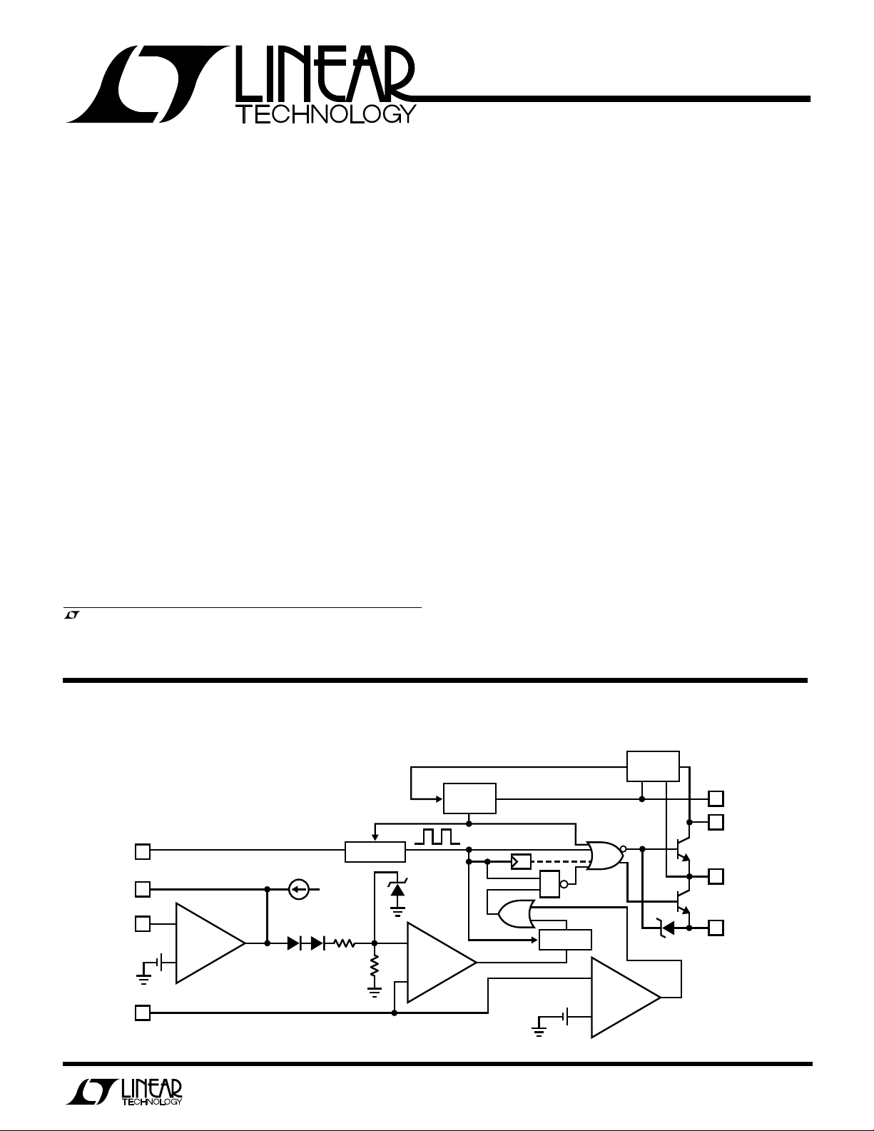
BLOCK
R
T/CT
COMP
FB
I
SENSE
IDAGRA
4
1
–
2
2.5V
+
3
W
1mA
5.6V
2R
OSCILLATOR
R
UV
OUTPUT
PULL-DOWN
+
–
LOCKOUT
18V
8
V
REF
7V
CC
6 OUTPUT
5 GND
1241 BD01
REFERENCE ENABLE
5V REF
MAIN BIAS
1V
–
+
REFERENCE PULL-DOWN
T
S
R
BLANKING
1.5V
1
Page 2
LT1241 Series
WU
U
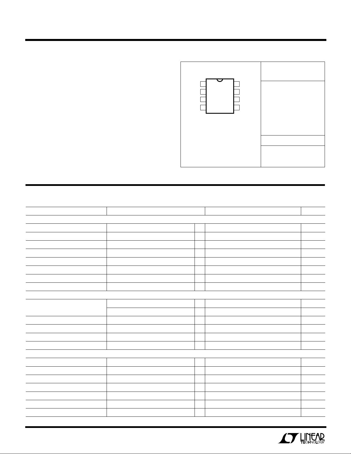
PACKAGE
/
O
RDER I FOR ATIO
COMP
FB
I
SENSE
R
T/CT
V
REF
V
CC
OUTPUT
GND
S8 PACKAGE
8-LEAD PLASTIC SO
N8 PACKAGE
8-LEAD PDIP
J8 PACKAGE
8-LEAD CERDIP
1
2
3
4
8
7
6
5
TOP VIEW
A
Supply Voltage ........................................................ 25V
Output Current.......................................................±1A*
Output Energy (Capacitive Load per Cycle)...............5µJ
Analog Inputs (Pins 2, 3)...............................–0.3 to 6V
Error Amplifier Output Sink Current...................... 10mA
Power Dissipation at TA ≤ 25°C ................................ 1W
Operating Junction Temperature Range
Storage Temperature Range ................. – 65°C to 150°C
Lead Temperature (Soldering, 10 sec)..................300°C
*The 1A rating for output current is based on transient switching
requirements.
E
PARAMETER CONDITIONS MIN TYP MAX UNITS
Reference Section
Output Voltage IO = 1mA, TJ = 25°C 4.925 5.000 5.075 V
Line Regulation 12V < VCC < 25V ● 320mV
Load Regulation 1mA < I
Temperature Stability 0.1 mV/°C
Total Output Variation Line, Load, Temp ● 4.87 5.13 V
Output Noise Voltage 10Hz < F < 10kHz, TJ = 25°C50µV
Long Term Stability TA = 125°C, 1000 Hrs. 5 25 mV
Output Short-Circuit Current ● –30 –90 –180 mA
Oscillator Section
Initial Accuracy RT = 10k, CT = 3.3nF, TJ = 25°C 47.5 50 52.5 kHz
Voltage Stability 12V < VCC < 25V, TJ = 25°C1%
Temperature Stability T
Amplitude TJ = 25°C (Pin 4) 1.7 V
Clock Ramp Reset Current V
Error Amplifier Section
Feedback Pin Input Voltage V
Input Bias Current VFB = 2.5V ● –2 µA
Open-Loop Voltage Gain 2 < VO < 4V ● 65 90 dB
Unity-Gain Bandwidth TJ = 25°C 0.7 1.3 2 MHz
Power Supply Rejection Ratio 12V < VCC < 25V ● 60 dB
Output Sink Current V
Output Source Current V
2
W
O
LUTEXI T
S
A
WUW
ARB
U
G
I
S
LT124XC ............................................. 0°C to 100°C
LT124XI......................................... – 40°C to 100°C
LT124XM........................................ – 55°C to 125°C
LECTRICAL C CHARA TERIST
VREF
RT = 13.0k, CT = 500pF, TJ = 25°C 228 248 268 kHz
< TJ < T
MIN
(Pin 4) = 2V, TJ = 25°C 7.9 8.2 8.5 mA
OSC
= 2.5V ● 2.42 2.50 2.58 V
PIN1
= 2.7V, V
PIN2
= 2.3V, V
PIN2
ICS
< 20mA ● –6 –25 mV
MAX
(Notes 1, 2)
= 1.1V ● 26 mA
PIN1
= 5V ● –0.5 –0.75 mA
PIN1
T
= 125°C, θJA = 100°C/W (J8)
JMAX
= 100°C, θJA = 130°C/W (N8)
T
JMAX
= 100°C, θJA = 150°C/W (S8)
T
JMAX
ORDER PART
NUMBER
LT124XCJ8
LT124XCN8
LT124XCS8
LT124XIN8
LT124XIS8
LT124XMJ8
S8 PART MARKING
124X
124XI
–0.05 %/°C
Page 3

LT1241 Series
LECTRICAL C CHARA TERIST
E
PARAMETER CONDITIONS MIN TYP MAX UNITS
Error Amplifier Section
Output Voltage High Level V
Output Voltage Low Level V
Current Sense Section
Gain ● 2.85 3.00 3.15 V/V
Maximum Current Sense Input Threshold V
Power Supply Rejection Ratio ● 70 dB
Input Bias Current ● –1 10 µA
Delay to Output ● 50 100 ns
Blanking Time 100 ns
Blanking Override Voltage 1.5 V
Output Section
Output Low Level I
Output High Level I
Rise Time CL = 1nF, TJ = 25°C5080ns
Fall Time CL = 1.0nF, TJ = 25°C3060ns
Output Clamp Voltage IO = 1mA ● 18 19.5 V
Undervoltage Lockout
Start-Up Threshold
LT1241
LT1242/LT1244
LT1243/LT1245
Minimum Operating Voltage
LT1241/LT1243/LT1245 ● 7.0 7.6 8.2 V
LT1242/LT1244
Hysteresis
LT1241 1.6 2.0 V
LT1242/LT1244 5.5 6.0 V
LT1243/LT1245 0.4 0.8 V
PWM
Maximum Duty Cycle
LT1241/LT1244/LT1245 T
LT1242/LT1243 T
Minimum Duty Cycle ● 0%
Total Device
Start-Up Current ● 170 250 µA
Operating Current ● 710 mA
PIN2
PIN2
PIN3
= 20mA ● 0.25 0.4 V
OUT
= 200mA ● 0.75 2.2 V
I
OUT
= 20mA ● 12.0 V
OUT
= 200mA ● 11.75 V
I
OUT
= 25°C4648%
J
= 25°C9496%
J
ICS
= 2.3V, RL = 15k to GND ● 5 5.6 V
= 2.7V, RL = 15k to Pin 8 ● 0.2 1.1 V
< 1.1V ● 0.90 1.00 1.10 V
(Notes 1, 2)
● 9.0 9.6 10.2 V
● 15 16 17 V
● 7.8 8.4 9.0 V
● 9.0 10 11 V
The ● denotes those specifications which apply over the full operating
temperature range.
Note 1: Unless otherwise specified, V
= 15V, RT = 10k, CT = 3.3nF.
CC
Note 2: Low duty cycle pulse techniques are used during test to maintain
junction temperature close to ambient.
3
Page 4
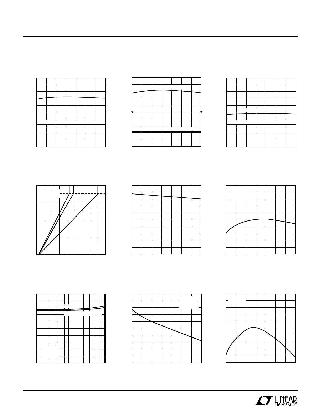
LT1241 Series
TEMPERATURE (°C)
–50
6
V
CC
(V)
7
8
9
10
11
–25 25 75 125
LT1241 • TPC03
0 50 100
MINIMUM OPERATING VOLTAGE
START-UP THRESHOLD
TEMPERATURE (°C)
–50
5
I
CC
(mA)
6
7
8
9
10
–25 25 75 125
LT1241 • TPC06
0 50 100
VCC = 15V
R
T
= 10k
C
T
= 3300pF
TEMPERATURE (°C)
–50
7.7
OSCILLATOR SINK CURRENT (mA)
8.7
–25 25 75 125
LT1241 • TPC08
0 50 100
7.8
8.0
8.2
8.4
8.6
8.5
7.9
8.1
8.3
V
PIN4
= 2V
UW
Y
PICA
11
LPER
F
O
R
AT
CCHARA TERIST
E
C
ICS
Undervoltage Lockout – Undervoltage Lockout –
Undervoltage Lockout – LT1241 LT1242, LT1244 LT1243, LT1245
17
START-UP THRESHOLD
MINIMUM OPERATING VOLTAGE
0 50 100
–25 25 75 125
TEMPERATURE (°C)
LT1241 • TPC02
(V)
CC
V
10
9
8
7
6
–50
START-UP THRESHOLD
MINIMUM OPERATING VOLTAGE
–25 25 75 125
0 50 100
TEMPERATURE (°C)
LT1241 • TPC01
(V)
CC
V
16
15
11
10
9
–50
Start-Up Current Start-Up Current Supply Current
200
180
160
140
120
100
80
60
START-UP CURRENT (µA)
40
20
0
–50
–25 25 75 125
0 50 100
TEMPERATURE (°C)
LT1241 • TPC05
START-UP CURRENT (µA)
200
START-UP
THRESHOLD
150
LT1243/5
100
50
0
0
410146 16
2 8 12 18
LT1241
VCC (V)
LT1242/4
TJ = 25°C
LT1241 • TPC04
Supply Current vs
Oscillator Frequency Oscillator Frequency Oscillator Sink Current
10
9
8
7
6
5
4
3
SUPPLY CURRENT (mA)
VCC = 15V
2
= 10k
R
T
= 15pF
C
1
L
0
10k
4
OSCILLATOR FREQUENCY (Hz)
LT1242, LT1243
LT1241, LT1244, LT1245
100k 1M
LT1241 • TPC18
60
58
56
54
52
50
48
FREQUENCY (kHz)
46
44
42
40
–25 25 75 125
–50
VCC = 5V
= 10k
R
T
= 3300pF
C
T
0 50 100
TEMPERATURE (°C)
LT1241 • TPC07
Page 5
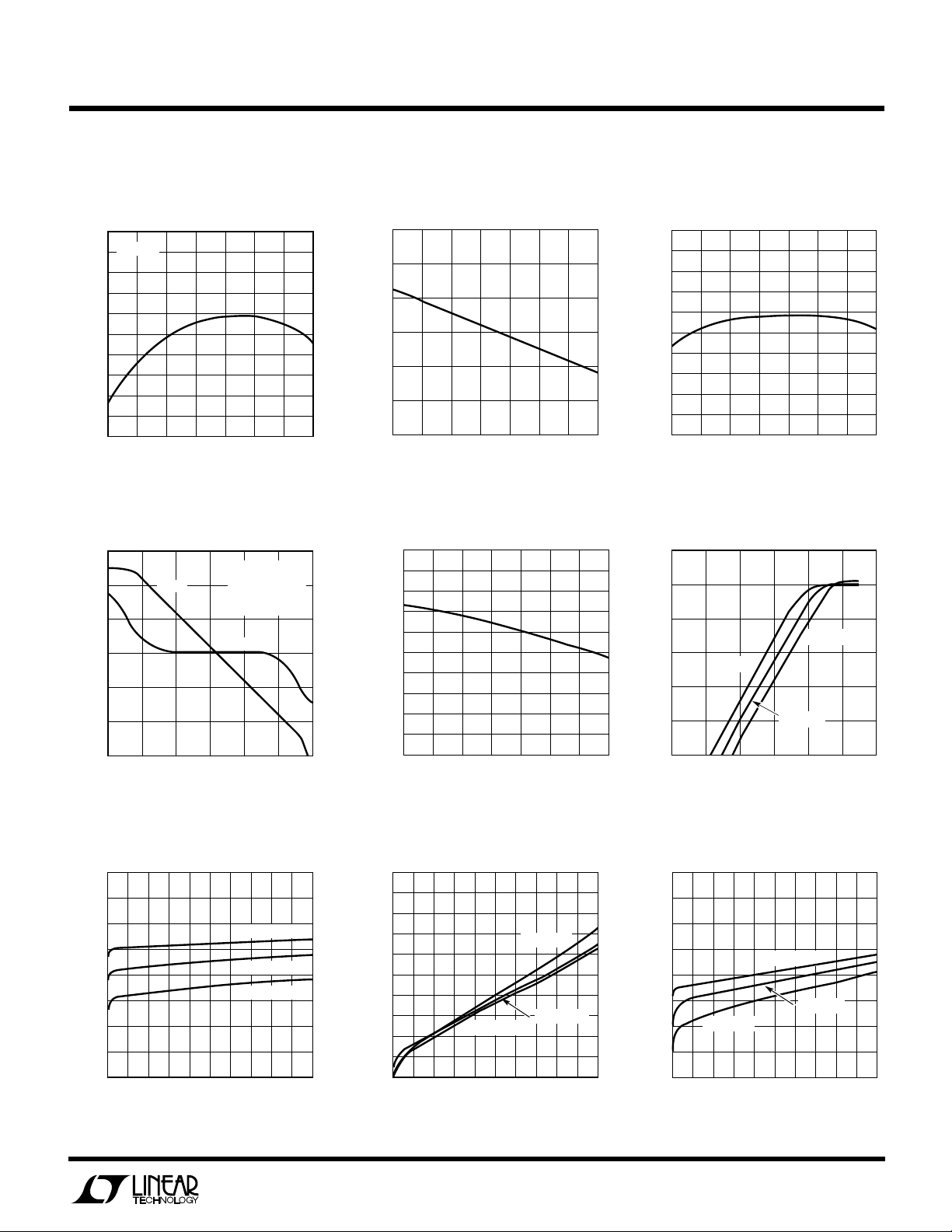
Y
OUTPUT SINK CURRENT (mA)
0
0
OUTPUT SATURATION VOLTAGE (V)
4.0
510
LT1241 • TPC15
2.0
0.5
1.0
1.5
2.5
3.0
3.5
TJ = 125°C
TJ = –55°C
TJ = 25°C
PICA
LPER
Reference Voltage Reference Short-Circuit Current Feedback Pin Input Voltage
5.05
IO = 1mA
5.04
5.03
5.02
5.01
5.00
4.99
4.98
REFERENCE VOLTAGE (V)
4.97
4.96
4.95
–50
–25 25 75 125
Error Amplifier Open-Loop Gain
and Phase Current Sense Clamp Voltage Current Sense Input Threshold
100
80
60
40
20
OPEN-LOOP VOLTAGE GAIN (dB)
0
VOL
A
–20
10
100 1k 100k 1M
High Level Output Low Level Output Voltage During Undervoltage
Saturation Voltage Saturation Voltage Lockout
4.0
3.5
3.0
2.5
2.0
1.5
1.0
OUTPUT SATURATION VOLTAGE (V)
0.5
0
0
OUTPUT SOURCE CURRENT (mA)
R
F
O
0 50 100
TEMPERATURE (°C)
LT1241 • TPC10
VCC = 15V
= 2.0V - 4.0V
V
GAIN
FREQUENCY (Hz)
O
= 100k
R
L
= 25°C
T
A
PHASE
10k 10M
LT1241 • TPC16
TJ = –55°C
TJ = 25°C
TJ = 125°C
100
LT1241 • TPC13
AT
200
UW
CCHARA TERIST
E
C
140
120
100
80
60
40
REFERENCE SHORT-CIRCUIT CURRENT (mA)
20
–50
225
180
135
90
45
0
–45
1.05
1.04
1.03
1.02
PHASE (DEG)
1.01
1.00
0.99
0.98
0.97
CURRENT SENSE CLAMP VOLTAGE (V)
0.96
0.95
–50
1.0
0.5
OUTPUT SATURATION VOLTAGE (V)
0
0
0 50 100
–25 25 75 125
TEMPERATURE (°C)
–25 25 75 125
OUTPUT SINK CURRENT (mA)
ICS
LT1241 • TPC09
0 50 100
TEMPERATURE (°C)
LT1241 • TPC12
TJ = 125°C
TJ = 25°C
100 200
TJ = –55°C
LT1241 • TPC14
LT1241 Series
2.55
2.54
2.53
2.52
2.51
2.50
2.49
2.48
2.47
FEEDBACK PIN INPUT VOLTAGE (V)
2.46
2.45
–50
1.2
1.0
0.8
0.6
0.4
0.2
CURRENT SENSE INPUT THRESHOLD (V)
0
0
Low Level Output Saturation
0 50 100
–25 25 75 125
TEMPERATURE (°C)
TJ = –55°C
=125°C
T
J
TJ = 25°C
12 45
ERROR AMP OUTPUT VOLTAGE (V)
36
LT1241 • TPC11
LT1241 • TPC17
5
Page 6

LT1241 Series
OSCILLATOR FREQUENCY (Hz)
10k
1
R
T
(kΩ)
10
100
100k 1M
LT1241 • TPC21
5nF
2nF
500pF
100pF
CT =10nF
1nF
200pF
VCC = 15V
T
J
= 25°C
UW
Y
PICA
60
LPER
F
O
R
AT
CCHARA TERIST
E
C
ICS
Output Deadtime vs Oscillator Output Deadtime vs Oscillator Timing Resistor vs Oscillator
Frequency – LT1242, LT1244 Frequency – LT1241, LT1243,LT1245 Frequency
75
50
40
30
% OF DEADTIME
20
10
0
0
5nF 2nF 1nF
500pF
100pF
100 1000
OSCILLATOR FREQUENCY (kHz)
LT1241 • TPC19
70
65
60
% OF DEADTIME
55
50
0
5nF 2nF
10nF 1nF
500pF
100 1000
OSCILLATOR FREQUENCY (kHz)
LT1241 • TPC20
100pF
Output Rise and Fall Time Output Cross-Conduction Current Current Sense Delay
OUTPUT VOLTAGE
VCC = 15V
C
= 1nF
L
TIME 50ns/DIV
LT1241 • TPC22
5V/DIV
OUTPUT
VOLTAGE
20mA/DIV
OUTPUT CROSS-
CONDUCTION CURRENT
= 15V
V
CC
C
= 15pF
L
TIME 50ns/DIV
LT1241 • TPC23
5V/DIV
OUTPUT
VOLTAGE
1V/DIV
CURRENT
SENSE INPUT
V
C
CC
= 1nF
L
= 15V
TIME 50ns/DIV
LT1241 • TPC24
6
Page 7

LT1241 Series
U
PI
COMP (Pin 1): Compensation Pin. This pin is the output of
the Error Amplifier and is made available for loop compensation. It can also be used to adjust the maximum value of
the current sense clamp voltage to less than 1V. This pin
can source a minimum of 0.5mA (0.8mA typ) and sink a
minimum of 2mA (4mA typ)
FB (Pin 2) Voltage Feedback Pin. This pin is the inverting
input of the error amplifier. The output voltage is normally
fed back to this pin through a resistive divider. The noninverting input of the error amplifier is internally committed to a 2.5V reference point.
I
current sense comparator. The trip point of the comparator is set by, and is proportional to, the output voltage of
the Error Amplifier.
RT/CT (Pin 4): The oscillator frequency and the deadtime
are set by connecting a resistor (RT) from V
and a capacitor (CT) from RT/CT to GND.
FUUC
(Pin 3): Current Sense Pin. This is the input to the
SENSE
TI
O
U
S
REF
to RT/C
T
The rise time of the oscillator waveform is set by the RC
time constant of RT and CT. The fall time, which is equal to
the output deadtime, is set by a combination of the RC time
constant and the oscillator sink current (8.2mA typ).
GND (Pin 5): Ground.
OUTPUT (Pin 6): This pin is the output of a high current
totem pole output stage. It is capable of driving up to ±1A
of current into a capacitive load such as the gate of a
MOSFET.
V
(Pin 7): This pin is the positive supply of the control
CC
IC.
V
(Pin 8): Reference. This is the reference output of the
REF
IC. The reference output is used to supply charging current
to the external timing resistor RT. The reference provides
biasing to a large portion of the internal circuitry, and is
used to generate several internal reference levels including the VFB level and the current sense clamp voltage.
U
O
PPLICATI
A
MINIMUM
START-UP OPERATING MAXIMUM
DEVICE THRESHOLD VOLTAGE DUTY CYCLE REPLACES
LT1241 9.6V 7.6V 50% NONE
LT1242 16V 10V 100% UC1842
LT1243 8.4V 7.6V 100% UC1843
LT1244 16V 10V 50% UC1844
LT1245 8.4V 7.6V 50% UC1845
Oscillator
The LT1241 series devices are fixed frequency current
mode pulse width modulators. The oscillator frequency
and the oscillator discharge current are both trimmed and
tightly specified to minimize the variations in frequency
and deadtime. The oscillator frequency is set by choosing
a resistor and capacitor combination, RT and CT. This RC
combination will determine both the frequency and the
maximum duty cycle. The resistor RT is connected from
V
(Pin 8) to the RT/CT pin (Pin 4). The capacitor CT is
REF
S
I FOR ATIO
WU
U
connected from the RT/CT pin to ground. The charging
current for CT is determined by the value of RT. The
discharge current for CT is set by the difference between
the current supplied by RT and the discharge current of the
LT124X. The discharge current of the device is trimmed to
8.2mA. For large values of RT discharge time will be
determined by the discharge current of the device and the
value of CT. As the value of RT is reduced it will have more
effect on the discharge time of CT. During an oscillator
cycle capacitor CT is charged to approximately 2.8V and
discharged to approximately 1.1V. The output is enabled
during the charge time of CT and disabled, in an off state,
during the discharge time of CT. The deadtime of the circuit
is equal to the discharge time of CT. The maximum duty
cycle is limited by controlling the deadtime of the oscillator. There are many combinations of RT and CT that will
yield a given oscillator frequency, however there is only
one combination that will yield a specific deadtime at that
frequency. Curves of oscillator frequency and deadtime
7
Page 8

LT1241 Series
U
O
PPLICATI
A
for various values of RT and CT appear in the Typical
Performance Characteristics section. Frequency and
deadtime can also be calculated using the following
formulas:
Oscillator Rise Time: tr = 0.583 • RC
Oscillator Discharge Time:
Oscillator Period: T
Oscillator Frequency:
Maximum Duty Cycle:
LT1241, LT1244, LT1245
t
D
LT1242, LT1243
The above formulas will give values that will be accurate
to approximately ±5%, at the oscillator, over the full
operating frequency range. This is due to the fact that the
oscillator trip levels are constant versus frequency and the
discharge current and initial oscillator frequency are
trimmed. Some fine adjustment may be required to achieve
more accurate results. Once the final RT/CT combination is
selected the oscillator characteristics will be repeatable
from device to device. Note that there will be some slight
differences between maximum duty cycle at the oscillator
and maximum duty cycle at the output due to the finite rise
and fall times of the output.
The output switching frequency will be equal to the
oscillator frequency for LT1242 and LT1243. The output
switching frequency will be equal to one-half the oscillator
==
MAX
T
22
r
OSC
S
I FOR ATIO
t
=
d
= tr + t
OSC
f
OSC
Tt
OSC d
D
MAX
d
=
T
OSC
−
T
OSC
t
r
==
T
OSC
WU
346
.
0 0164 11 73
..
()
1
R
Tt
−
OSC d
T
OSC
RC
•
−
U
frequency for LT1241, LT1244 and LT1245. The oscillator
of LT1241 series devices will run at frequencies up to
1MHz, allowing 500kHz output switching frequencies for
all devices.
Error Amplifier
The LT1241 series of devices contain a fully compensated
error amplifier with a DC gain of 90dB and a unity-gain
frequency of 1MHz. Phase margin at unity-gain is 80°. The
noninverting input is internally committed to a 2.5V reference point derived from the 5V reference of Pin 8. The
inverting input (Pin 2) and the output (Pin 1) are made
available to the user. The output voltage in a regulator
circuit is normally fed back to the inverting input of the
error amplifier through a resistive divider.
The output of the error amplifier is made available for
external loop compensation. The output current of the
error amplifier is limited to approximately 0.8mA sourcing
and approximately 6mA sinking. In a current mode PWM
the peak switch current is a function of the output voltage
of the error amplifier. In the LT1241 series devices the
output of the error amplifier is offset by two diodes (1.4V
at 25°C), divided by a factor of three, and fed to the
inverting input of the current sense comparator. For error
amplifier output voltages less than 1.4V the duty cycle of
the output stage will be zero. The maximum offset that can
appear at the current sense input is limited by a 1V clamp.
This occurs when the error amplifier output reaches 4.4V
at 25°C.
The output of the error amplifier can be clamped below
4.4V in order to reduce the maximum voltage allowed
across the current sensing resistor to less than 1V. The
supply current will increase by the value of the output
source current when the output voltage of the error
amplifier is clamped.
8
Page 9

LT1241 Series
U
O
PPLICATI
A
Current Sense Comparator and PWM Latch
LT1241 series devices are current mode controllers.
Under normal operating conditions the output (Pin 6) is
turned on at the start of every oscillator cycle, coincident
with the rising edge of the oscillator waveform. The output
is then turned off when the current reaches a threshold
level proportional to the error voltage at the output of the
error amplifier. Once the output is turned off it is latched
off until the start of the next cycle. The peak current is thus
proportional to the error voltage and is controlled on a
cycle by cycle basis. The peak switch current is normally
sensed by placing a sense resistor in the source lead of the
output MOSFET. This resistor converts the switch current
to a voltage that can be fed into the current sense input. For
normal operating conditions the peak inductor current,
which is equal to the peak switch current, will be equal to:
VV
()
PIN
I
=
PK
1
()
During fault conditions the maximum threshold voltage at
the input of the current sense comparator is limited by the
internal 1V clamp at the inverting input. The peak switch
current will be equal to:
10
I
PK MAX
In certain applications, such as high power regulators, it
may be desirable to limit the maximum threshold voltage
to less than 1V in order to limit the power dissipated in the
sense resistor or to limit the short-circuit current of the
regulator circuit. This can be accomplished by clamping
the output of the error amplifier. A voltage level of
approximately 1.4V at the output of the error amplifier will
give a threshold voltage of 0V. A voltage level of approximately 4.4V at the output of the error amplifier will give
a threshold level of 1V. Between 1.4V and 4.4V the
threshold voltage will change by a factor of one-third of the
=
()
S
−
143.
R
S
.
V
R
S
I FOR ATIO
WU
U
change in the error amplifier output voltage. The threshold
voltage will be 0.333V for an error amplifier voltage of
2.4V. To reduce the maximum current sense threshold to
less than 1V the error amplifier output should be clamped
to less than 4.4V.
Blanking
A unique feature of the LT1241 series devices is the builtin blanking circuit at the output of the current sense
comparator. A common problem with current mode
PWM circuits is erratic operation due to noise at the
current sense input. The primary cause of noise problems
is the leading edge current spike due to transformer
interwinding capacitance and diode reverse recovery
time. This current spike can prematurely trip the current
sense comparator causing an instability in the regulator
circuit. A filter at the current sense input is normally
required to eliminate this instability.
This filter will in turn slow down the current sense loop.
A slow current sense loop will increase the minimum pulse
width which will increase the short-circuit current in an
overload condition. The LT1241 series devices blank (lock
out) the signal at the output of the current sense comparator for a fixed amount of time after the switch is turned on.
This effectively prevents the PWM latch from tripping due
to the leading edge current spike.
The blanking time will be a function of the voltage at the
feedback pin (Pin 2). The blanking time will be 100ns for
normal operating conditions (VFB = 2.5V). The blanking
time goes to zero as the feedback pin is pulled to 0V. This
means that the blanking time will be minimized during
start-up and also during an output short-circuit fault. This
blanking circuit eliminates the need for an input filter at the
current sense input except in extreme cases. Eliminating
the filter allows the current sense loop to operate with
minimum delays, reducing peak currents during fault
conditions.
9
Page 10

LT1241 Series
U
O
PPLICATI
A
Undervoltage Lockout
The LT1241 series devices incorporate an undervoltage
lockout comparator which prevents the internal reference
circuitry and the output from starting up until the supply
voltage reaches the start-up threshold voltage. The quiescent current, below the start-up threshold, has been
reduced to less than 250µA (170µA typ.) to minimize the
power loss due to the bleed resistor used for start-up in
off-line converters. In undervoltage lockout both V
(Pin 8) and the output (Pin 6) are actively pulled low by
Darlington connected PNP transistors. They are designed
to sink a few milliamps of current and will pull down to
about 1V. The pull-down transistor at the reference pin can
be used to reset the external soft start capacitor. The pulldown transistor at the output eliminates the external pulldown resistor required, with earlier devices, to hold the
external MOSFET gate low during undervoltage lockout.
Output
The LT1241 series devices incorporate a single high
current totem pole output stage. This output stage is
capable of driving up to ± 1A of output current. Crossconduction current spikes in the output totem pole have
been eliminated. This device is primarily intended for
driving MOSFET switches. Rise time is typically 40ns and
fall time is typically 30ns when driving a 1.0nF load. A
clamp is built into the device to prevent the output from
rising above 18V in order to protect the gate of the
MOSFET switch.
The output is actively pulled low during undervoltage
lockout by a Darlington PNP. This PNP is designed to sink
several milliamps and will pull the output down to approximately 1V. This active pull-down eliminates the need for an
external resistor which was required in older designs. The
output pin of the device connects directly to the emitter of
the upper NPN drive transistor and the collector of the
lower NPN drive transistor in the totem pole. The collector
of the lower transistor, which is n-type silicon, forms a
p-n junction with the substrate of the device. This junction
is reverse biased during normal operation.
S
I FOR ATIO
WU
U
REF
ground. If the OUTPUT pin is pulled negative by more than
a diode drop the parasitic diode formed by the collector of
the output NPN and the substrate will turn on. This can
cause erratic operation of the device. In these cases a
Schottky clamp diode is recommended from the output to
ground.
Reference
The internal reference of the LT1241 series devices is a 5V
bandgap reference, trimmed to within ±1% initial toler-
ance. The reference is used to power the majority of
internal logic and the oscillator circuitry. The oscillator
charging current is supplied from the reference. The
feedback pin voltage and the clamp level for the current
sense comparator are derived from the reference voltage.
The reference can supply up to 20mA of current to power
external circuitry. Note that using the reference in this
manner, as a voltage regulator, will significantly increase
power dissipation in the device which will reduce the
useful operating ambient temperature range.
Design/Layout Considerations
LT1241 series devices are high speed circuits capable of
generating pulsed output drive currents of up to 1A peak.
The rise and fall time for the output drive current is in the
range of 10ns to 20ns. High speed circuit techniques must
be used to insure proper operation of the device. Do not
attempt to use Proto-boards or wire-wrap techniques to
breadboard high speed switching regulator circuits.
They
will not
Printed circuit layouts should include separate ground
paths for the voltage feedback network, oscillator capacitor, and switch drive current. These ground paths should
be connected together directly at the ground pin (Pin 5) of
the LT124X. This will minimize noise problems due to
pulsed ground pin currents. VCC should be bypassed, with
a minimum of 0.1µF, as close to the device as possible.
High current paths should be kept short and they should
be separated from the feedback voltage network with
shield traces if possible.
work properly.
In some applications the parasitic LC of the external
MOSFET gate can ring and pull the OUTPUT pin below
10
Page 11

LT1241 Series
U
O
PPLICATITYPICAL
SA
External Clock Synchronization
V
REF
8
R
T
RT/C
100k
47Ω
C
4
T
V
R
COMP
EXTERNAL
SYNC
INPUT
0.01µF
+
D1 IS REQUIRED IF THE SYNC AMPLITUDE IS LARGE
ENOUGH TO PULL THE BOTTOM OF C
300mV BELOW GROUND.
R2
C
R1
T
REF
8
T/CT
4
1
FB
2
5V REF
OSCILLATOR
D1
MORE THAN
T
LT1241 • TA01
–
+
2.5V
V
REF
8
R
COMP
1
C
FB
2
–
1mA
+
I
SENSE
3
2.5V
Adjustable Clamp Level with Soft Start
REFERENCE ENABLE
REFERENCE PULL-DOWN
T
BLANKING
1mA
OSCILLATOR
5.6V
2R
5V REF
MAIN BIAS
1V
–
R
+
Soft Start
5.6V
2R
PULL-DOWN
S
R
1.5V
5V REF
R
LOCKOUT
OUTPUT
+
–
UV
1V
–
+
18V
1.5V
V
CC
7
OUTPUT
6
GND
5
I
SENSE
3
+
–
LT1241 • TA02
V
IN
R
S
≈
V
CLAMP
1.67
R2
+ 1
(
R1
(
I
PK (MAX)
≈
V
CLAMP
R
S
WHERE: 0V ≤ V
CLAMP
≤ 1.0V t
SOFT START
= –ln 1 –
3 • V
V
C
CLAMP
C
R1 R2
R1 + R2
LT1241 • TA03
11
Page 12

LT1241 Series
PPLICATITYPICAL
O
U
SA
300kHz Off-Line Power Supply
90VAC
TO
240VAC
HOT
NEU
AC GND
R5
1M
1/2W
D7
BAV21
C2
0.1µF
250V
MP3-X2
13
T1
BALEN
24
1212-R6103
COILTRONICS
R
T1
MCID404
2KBPOO5M
C14
+
100µF
400V
D6
1N5245B
15V
R7
510
1/10W
R1
200k
1/2W
R3
200k
1/2W
C3
0.1µF
250V
MP3-X2
C5
4700pF
250V
Y-CAP
R2
660k
1/10W
R4
660k
1/10W
C4
4700pF
250V
Y-CAP
4700pF
250V
Y-CAP
C1
470pF
–
C6
R5
27k
2W
D1
MUR160
D5
+
2KBPO8M
30T
30T
13T
T2
8
2
7
1
3
6
LP = 100µH
D3
MUR420
4
12T
5
CTX210433-1
L1
5 1/2 TURN
AIRCORE
C15
3.3µF
50V
C16
3.3µF
50V
R15
750Ω
1W
C13
4700pF
1kV
Y-CAP
LT1241 • TA06
20V
1.5A
RTN
R8
152k
R10
20k
12
C7
0.22µF
MKS-2
C9
0.01µF, 100V
R9
200k
R13
12k
C11
220pF
MKS-2
C10
0.1µF
MKS-2
NOTES: UNLESS OTHERWISE SPECIFIED
1. ALL RESISTANCES ARE IN OHMS, 1/4W, 5%.
2. ALL CAPACITANCES ARE IN MICROFARADS, 50V, 10%.
2
1
8
4
C8
100pF
FB
COMP
V
REF
R
T/CT
LT1241
OUTPUT
GND
I
5
V
SENSE
D4
BAT 85
R18
2Ω
1/4W
D2
BAV21
R11
12
R16
2Ω
1/4W
Q1
MPT2N60
R17
2Ω
1/4W
R14
39
R12
1k
1/10W
C12
22µF
25V
7
CC
6
3
Page 13

LT1241 Series
U
O
PPLICATITYPICAL
SA
V
REF
8
R
T
R
T/CT
4
C
T
COMP
1
FB
2
–
+
2.5V
PACKAGEDESCRIPTI
O
Slope Compensation at I
5V REF
MAIN BIAS
OSCILLATOR
5.6V
1mA
2R
1V
–
R
+
Pin
SENSE
REFERENCE ENABLE
REFERENCE PULL-DOWN
T
S
R
BLANKING
PULL-DOWN
+
1.5V
UV
LOCKOUT
OUTPUT
18V
–
U
Dimensions in inches (millimeters) unless otherwise noted.
V
CC
7
OUTPUT
6
GND
5
I
SENSE
3
V
IN
R
LT1241 • TA04
S
J8 Package
8-Lead CERDIP (Narrow 0.300, Hermetic)
(LTC DWG # 05-08-1110)
CORNER LEADS OPTION
(4 PLCS)
0.023 – 0.045
(0.584 – 1.143)
HALF LEAD
0.045 – 0.068
(1.143 – 1.727)
FULL LEAD
OPTION
0.300 BSC
(0.762 BSC)
0.008 – 0.018
(0.203 – 0.457)
0.385 ± 0.025
(9.779 ± 0.635)
NOTE: LEAD DIMENSIONS APPLY TO SOLDER DIP/PLATE OR TIN PLATE LEADS.
0° – 15°
OPTION
0.005
(0.127)
MIN
0.025
(0.635)
RAD TYP
0.045 – 0.068
(1.143 – 1.727)
0.014 – 0.026
(0.360 – 0.660)
0.405
(10.287)
MAX
87
12
65
3
4
0.220 – 0.310
(5.588 – 7.874)
0.015 – 0.060
(0.381 – 1.524)
0.100 ± 0.010
(2.540 ± 0.254)
0.200
(5.080)
MAX
0.125
3.175
MIN
J8 0694
13
Page 14

LT1241 Series
PACKAGEDESCRIPTI
O
U
Dimensions in inches (millimeters) unless otherwise noted.
N8 Package
8-Lead PDIP (Narrow 0.300)
(LTC DWG # 05-08-1510)
0.400*
(10.160)
MAX
876
5
0.255 ± 0.015*
(6.477 ± 0.381)
0.300 – 0.325
(7.620 – 8.255)
0.065
(1.651)
0.009 – 0.015
(0.229 – 0.381)
+0.025
0.325
–0.015
+0.635
8.255
()
–0.381
*THESE DIMENSIONS DO NOT INCLUDE MOLD FLASH OR PROTRUSIONS.
MOLD FLASH OR PROTRUSIONS SHALL NOT EXCEED 0.010 INCH (0.254mm)
TYP
(2.540 ± 0.254)
12
0.045 – 0.065
(1.143 – 1.651)
0.005
(0.127)
MIN
0.100 ± 0.010
3
4
0.130 ± 0.005
(3.302 ± 0.127)
0.125
(3.175)
MIN
0.018 ± 0.003
(0.457 ± 0.076)
0.015
(0.380)
MIN
N8 0695
14
Page 15

PACKAGEDESCRIPTI
U
O
Dimensions in inches (millimeters) unless otherwise noted.
S8 Package
8-Lead Plastic Small Outline (Narrow 0.150)
(LTC DWG # 05-08-1610)
0.189 – 0.197*
(4.801 – 5.004)
7
8
LT1241 Series
5
6
0.010 – 0.020
(0.254 – 0.508)
0.008 – 0.010
(0.203 – 0.254)
*
DIMENSION DOES NOT INCLUDE MOLD FLASH. MOLD FLASH
SHALL NOT EXCEED 0.006" (0.152mm) PER SIDE
**
DIMENSION DOES NOT INCLUDE INTERLEAD FLASH. INTERLEAD
FLASH SHALL NOT EXCEED 0.010" (0.254mm) PER SIDE
× 45°
0°– 8° TYP
0.016 – 0.050
0.406 – 1.270
0.228 – 0.244
(5.791 – 6.197)
0.053 – 0.069
(1.346 – 1.752)
0.014 – 0.019
(0.355 – 0.483)
0.150 – 0.157**
(3.810 – 3.988)
1
3
2
4
(1.270)
0.004 – 0.010
(0.101 – 0.254)
0.050
BSC
SO8 0695
Information furnished by Linear Technology Corporation is believed to be accurate and reliable.
However, no responsibility is assumed for its use. Linear Technology Corporation makes no representation that the interconnection of its circuits as described herein will not infringe on existing patent rights.
15
Page 16

LT1241 Series
TYPICAL APPLICATION
V
REF
8
R
R
/
C
T
T
T
TO
V
OUT
R
SLOPE
4
C
T
COMP
1
R
f
2
FB
2.5V
U
Slope Compensation at Error Amp
UV
5V REF
MAIN BIAS
OSCILLATOR
5.6V
1mA
–
2R
+
1V
–
R
+
REFERENCE ENABLE
REFERENCE PULL-DOWN
T
S
R
BLANKING
1.5V
LOCKOUT
OUTPUT
PULL-DOWN
+
–
18V
V
OUTPUT
GND
I
SENSE
LT1241 • TA05
CC
7
6
5
3
RELATED PARTS
PART NUMBER DESCRIPTION COMMENTS
LT1246 1MHz Current Mode PWM 16V Start-Up Threshold, 10V Minimum Operating Voltage
LT1248/LT1249 Power Factor Controllers Minimal Parts Count
LT1372 High Efficiency Switching Regulator 500kHz 1.5A Boost Regulator
LT1376 1.5A 500kHz Step-Down Switching Regulator Steps Down from Up to 25V Using 4.7µH Inductors
LT1509 Power Factor and PWM Controller Complete Solution for Universal Off-Line Switching Power Supplies
16
Linear Technology Corporation
1630 McCarthy Blvd., Milpitas, CA 95035-7417 ● (408) 432-1900
FAX: (408) 434-0507
●
TELEX: 499-3977 ● www.linear-tech.com
1241fa LT/TP 0297 5K REV A • PRINTED IN USA
LINEAR TECHNOLOGY CORPORATION 1992
 Loading...