

Page 1
LT1228
100MHz Current Feedback
Amplifier with DC Gain Control
EATU
F
■
Very Fast Transconductance Amplifier
RE
S
Bandwidth: 75MHz
gm = 10 × I
Low THD: 0.2% at 30mV
Wide I
■
Very Fast Current Feedback Amplifier
SET
Range: 1µA to 1mA
SET
RMS
Input
Bandwidth: 100MHz
Slew Rate: 1000V/µs
Output Drive Current: 30mA
Differential Gain: 0.04%
Differential Phase: 0.1°
High Input Impedance: 25MΩ, 6pF
■
Wide Supply Range: ±2V to ±15V
■
Inputs Common Mode to Within 1.5V of Supplies
■
Outputs Swing Within 0.8V of Supplies
■
Supply Current: 7mA
U
O
PPLICATI
A
■
Video DC Restore (Clamp) Circuits
■
Video Differential Input Amplifiers
■
Video Keyer/Fader Amplifiers
■
AGC Amplifiers
■
Tunable Filters
■
Oscillators
S
DUESCRIPTIO
The LT1228 makes it easy to electronically control the gain
of signals from DC to video frequencies. The LT1228
implements gain control with a transconductance amplifier
(voltage to current) whose gain is proportional to an externally controlled current. A resistor is typically used to
convert the output current to a voltage, which is then
amplified with a current feedback amplifier. The LT1228
combines both amplifiers into an 8-pin package, and operates on any supply voltage from 4V (±2V) to 30V (±15V). A
complete differential input, gain controlled amplifier can be
implemented with the LT1228 and just a few resistors.
The LT1228 transconductance amplifier has a high impedance differential input and a current source output with wide
output voltage compliance. The transconductance, gm, is
set by the current that flows into pin 5, I
gm is equal to ten times the value of I
holds over several decades of set current. The voltage at pin
5 is two diode drops above the negative supply, pin 4.
The LT1228 current feedback amplifier has very high input
impedance and therefore it is an excellent buffer for the
output of the transconductance amplifier. The current feedback amplifier maintains its wide bandwidth over a wide
range of voltage gains making it easy to interface the
transconductance amplifier output to other circuitry. The
current feedback amplifier is designed to drive low impedance loads, such as cables, with excellent linearity at high
frequencies.
. The small signal
SET
and this relationship
SET
U
O
A
PPLICATITYPICAL
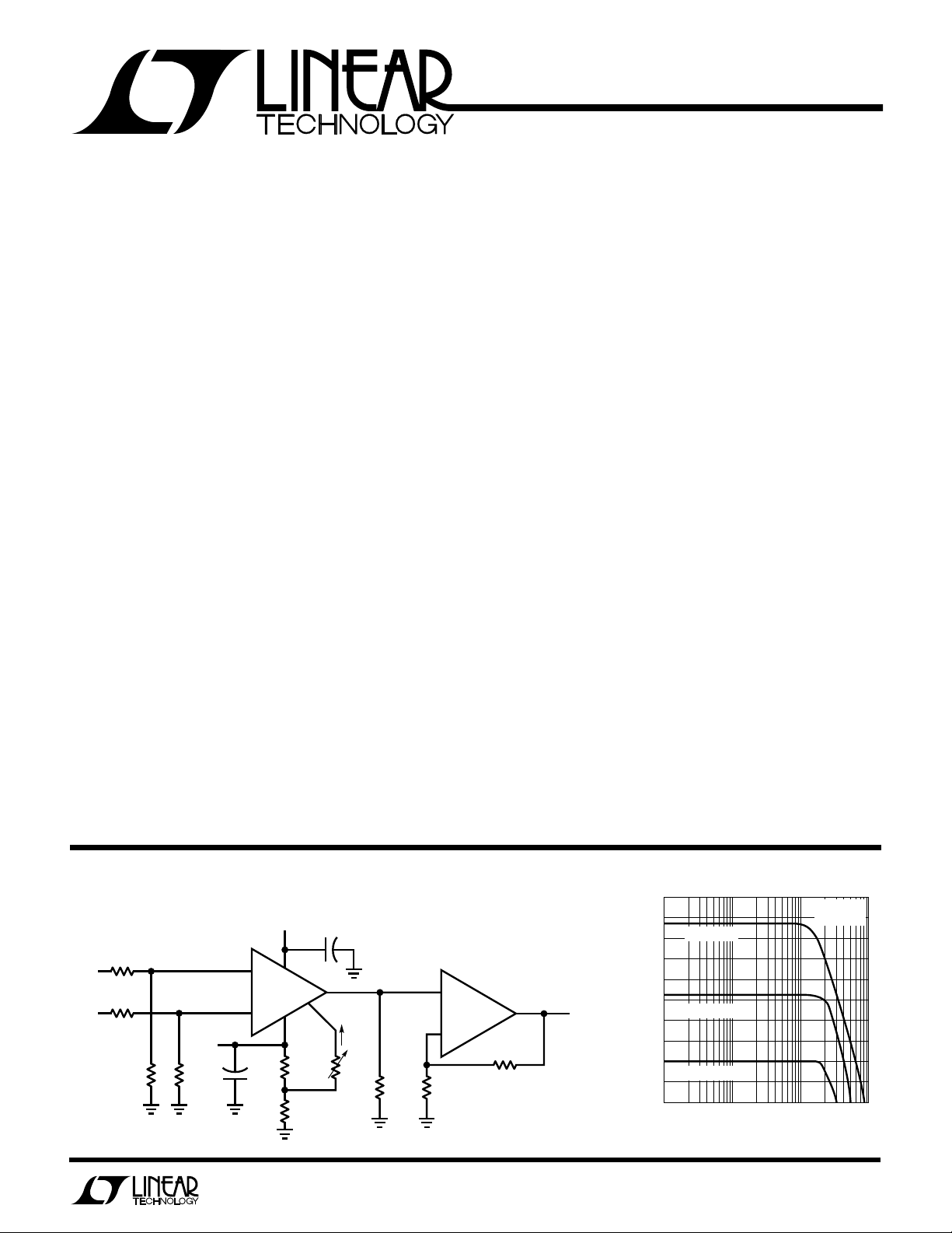
Differential Input Variable Gain Amp
15V
4.7µF
m
7
4
R4
1.24k
R6
6.19Ω
+
1
+
5
I
SET
R5
10k
R1
270Ω
CFA V
8
–
RG
10Ω
6
R
F
470Ω
HIGH INPUT RESISTANCE
EVEN WHEN POWER IS OFF
–18dB < GAIN < 2dB
≤ 3V
V
IN
RMS
OUT
LT1228 • TA01
R3A
10k
+
R2A
V
IN
10k
–
–15V
100Ω
R3
R2
100Ω
3
+
g
2
–
4.7µF
+
6
3
0
–3
–6
–9
GAIN (dB)
–12
–15
–18
–21
–24
100k
Frequency Response
= 1mA
I
SET
I
= 300µA
SET
I
= 100µA
SET
1M 10M 100M
FREQUENCY (Hz)
= ±15V
V
S
= 100Ω
R
L
LT1228 • TA02
1
Page 2
LT1228
WU
U
PACKAGE
/
O
RDER I FOR ATIO
W
O
A
LUTEXI T
S
Supply Voltage ...................................................... ±18V
Input Current, Pins 1, 2, 3, 5, 8 (Note 7) ............ ±15mA
Output Short Circuit Duration (Note 1) .........Continuous
Operating Temperature Range
LT1228C................................................ 0°C to 70°C
LT1228M........................................ –55°C to 125°C
Storage Temperature Range ................. –65°C to 150°C
Junction Temperature
Plastic Package .............................................. 150°C
Ceramic Package ............................................175°C
Lead Temperature (Soldering, 10 sec)..................300°C
LECTRICAL C CHARA TERIST
E
Current Feedback Amplifier, Pins 1, 6, 8. ±5V ≤ VS ≤ ±15V, I
SYMBOL PARAMETER CONDITIONS MIN TYP MAX UNITS
V
OS
+
I
IN
–
I
IN
e
n
i
n
R
IN
C
IN
CMRR Common-Mode Rejection Ratio VS = ±15V, V
PSRR Power Supply Rejection Ratio VS = ±2V to ±15V, TA = 25°C6080dB
Input Offset Voltage TA = 25°C ±3 ±10 mV
Input Offset Voltage Drift ● 10 µV/°C
Noninverting Input Current TA = 25°C ±0.3 ±3 µA
Inverting Input Current TA = 25°C ±10 ±65 µA
Input Noise Voltage Density f = 1kHz, RF = 1k, RG = 10Ω, RS = 0Ω 6 nV/√Hz
Input Noise Current Density f = 1kHz, RF = 1k, RG = 10Ω, RS = 10k 1.4 pV/√Hz
Input Resistance V
Input Capacitance (Note 2) VS = ±5V 6 pF
Input Voltage Range VS = ±15V, TA = 25°C ±13 ±13.5 V
Inverting Input Current VS = ±15V, V
Common-Mode Rejection V
Noninverting Input Current VS = ±2V to ±15V, TA = 25°C 10 50 nA/V
Power Supply Rejection V
Inverting Input Current VS = ±2V to ±15V, TA = 25°C 0.1 5 µA/V
Power Supply Rejection VS = ±3V to ±15V ● 5 µA/V
A
WUW
U
ARB
G
I
S
TOP VIEW
1I
OUT
2
–IN
+IN
–
V
J8 PACKAGE
8-LEAD CERAMIC DIP
T
T
J MAX =
T
J MAX =
Consult Factory for Industrial grade parts.
g
m
3
S8 PACKAGE
8-LEAD PLASTIC SOIC
175°C, θ
J MAX =
150°C, θ
150°C, θ
8
7
6
54
N8 PACKAGE
100°C/W (J)
100°C/W (N)
150°C/W (S)
GAIN
+
V
V
OUT
I
SET
+–
8-LEAD PLASTIC DIP
JA =
JA =
JA =
ORDER PART
NUMBER
LT1228MJ8
LT1228CJ8
LT1228CN8
LT1228CS8
S8 PART MARKING
1228
ICS
= 0µA, VCM = 0V unless otherwise noted.
SET
● ±15 mV
● ±10 µA
● ±100 µA
= ±13V, VS = ±15V ● 225 MΩ
IN
= ±3V, VS = ±5V ● 225 MΩ
V
IN
● ±12 V
VS = ±5V, TA = 25°C ±3 ±3.5 V
● ±2V
= ±13V, TA = 25°C5569dB
= ±15V, V
V
S
= ±5V, V
V
S
= ±5V, V
V
S
= ±15V, V
S
= ±5V, V
V
S
VS = ±5V, V
= ±3V to ±15V ● 60 dB
V
S
= ±3V to ±15V ● 50 nA/V
S
CM
= ±12V ● 55 dB
CM
= ±3V, TA = 25°C5569dB
CM
= ±2V ● 55 dB
CM
= ±13V, TA = 25°C 2.5 10 µA/V
CM
= ±12V ● 10 µA/V
CM
= ±3V, TA = 25°C 2.5 10 µA/V
CM
= ±2V ● 10 µA/V
CM
2
Page 3
LT1228
LECTRICAL C CHARA TERIST
E
Current Feedback Amplifier, Pins 1, 6, 8. ±5V ≤ VS ≤ ±15V, I
SYMBOL PARAMETER CONDITIONS MIN TYP MAX UNITS
A
V
R
OL
V
OUT
I
OUT
I
s
SR Slew Rate (Notes 3 and 5) TA = 25°C 300 500 V/µs
SR Slew Rate VS = ±15V, RF = 750Ω, RG= 750Ω, RL = 400Ω 3500 V/µs
t
r
BW Small-Signal Bandwidth VS = ±15V, RF = 750Ω, RG= 750Ω, RL = 100Ω 100 MHz
t
r
t
s
Large-Signal Voltage Gain VS = ±15V, V
Transresistance, ∆V
Maximum Output Voltage Swing VS = ±15V, R
Maximum Output Current R
Supply Current V
Rise Time (Notes 4 and 5) TA = 25°C1020ns
Small-Signal Rise Time VS = ±15V, RF = 750Ω, RG= 750Ω, RL = 100Ω 3.5 ns
Propagation Delay VS = ±15V, RF = 750Ω, RG= 750Ω, RL = 100Ω 3.5 ns
Small-Signal Overshoot VS = ±15V, RF = 750Ω, RG= 750Ω, RL = 100Ω 15 %
Settling Time 0.1%, V
Differential Gain (Note 6) VS = ±15V, RF = 750Ω, RG= 750Ω, RL = 1k 0.01 %
Differential Phase (Note 6) VS = ±15V, RF = 750Ω, RG= 750Ω, RL = 1k 0.01 DEG
Differential Gain (Note 6) VS = ±15V, RF = 750Ω, RG= 750Ω, RL = 150Ω 0.04 %
Differential Phase (Note 6) VS = ±15V, RF = 750Ω, RG= 750Ω, RL = 150Ω 0.1 DEG
OUT
/∆I
–
IN
ICS
= 0µA, VCM = 0V unless otherwise noted.
SET
= ±10V, R
VS = ±5V, V
VS = ±15V, V
= ±5V, V
V
S
= ±5V, R
V
S
LOAD
OUT
OUT
= ±2V, R
OUT
= ±10V, R
OUT
= ±2V, R
OUT
= 400Ω, TA = 25°C ±12 ±13.5 V
LOAD
= 150Ω, TA = 25°C ±3 ±3.7 V
LOAD
= 0Ω, TA = 25°C 30 65 125 mA
= 0V, I
= 0V ● 611 mA
SET
= 10V, RF =1k, RG= 1k, RL =1k 45 ns
OUT
= 1k ● 55 65 dB
LOAD
= 150Ω ● 55 65 dB
LOAD
= 1k ● 100 200 kΩ
LOAD
= 150Ω ● 100 200 kΩ
LOAD
● ±10 V
● ±2.5 V
● 25 125 mA
LECTRICAL C CHARA TERIST
E
Transconductance Amplifier, Pins 1, 2, 3, 5. ±5V ≤ VS ≤ ±15V, I
SYMBOL PARAMETER CONDITIONS MIN TYP MAX UNITS
V
OS
I
OS
I
B
e
n
R
IN
C
IN
Input Offset Voltage I
Input Offset Voltage Drift ● 10 µV/°C
Input Offset Current TA = 25°C 40 200 nA
Input Bias Current TA = 25°C 0.4 1 µA
Input Noise Voltage Density f = 1kHz 20 nV/√Hz
Input Resistance-Differential Mode V
Input Resistance-Common Mode VS = ±15V, VCM = ±12V ● 50 1000 MΩ
Input Capacitance 3pF
Input Voltage Range VS = ±15V, TA = 25°C ±13 ±14 V
ICS
= 100µA, VCM = 0V unless otherwise noted.
SET
= 1mA, TA = 25°C ±0.5 ±5mV
SET
≈ ±30mV ● 30 200 kΩ
IN
= ±5V, VCM = ±2V ● 50 1000 MΩ
V
S
= ±15V ● ±12 V
V
S
= ±5V, TA = 25°C ±3 ±4V
V
S
= ±5V ● ±2V
V
S
● ±10 mV
● 500 nA
● 5 µA
3
Page 4
LT1228
LECTRICAL C CHARA TERIST
E
Transconductance Amplifier, Pins 1, 2, 3, 5. ±5V ≤ VS ≤ ±15V, I
SYMBOL PARAMETER CONDITIONS MIN TYP MAX UNITS
CMRR Common-Mode Rejection Ratio VS = ±15V, V
PSRR Power Supply Rejection Ratio VS = ±2V to ±15V, TA = 25°C 60 100 dB
g
m
I
OUT
I
OL
V
OUT
R
O
I
S
THD Total Harmonic Distortion VIN = 30mV
BW Small-Signal Bandwidth R1 = 50Ω, I
t
r
Transconductance I
Transconductance Drift ● –0.33 %/°C
Maximum Output Current I
Output Leakage Current I
Maximum Output Voltage Swing VS = ±15V , R1 = ∞ ● ±13 ±14 V
Output Resistance VS = ±15V, V
Output Capacitance (Note 2) VS = ±5V 6 pF
Supply Current, Both Amps I
Small-Signal Rise Time R1 = 50Ω, I
Propagation Delay R1 = 50Ω, I
ICS
= 100µA, VCM = 0V unless otherwise noted.
SET
= ±13V, TA = 25°C 60 100 dB
= ±15V, V
V
S
= ±5V, V
V
S
VS = ±5V, V
= ±3V to ±15V ● 60 dB
V
S
= 100µA, I
SET
= 100µA ● 70 100 130 µA
SET
= 0µA (+IIN of CFA), TA = 25°C 0.3 3 µA
SET
= ±5V , R1 = ∞ ● ±3 ±4V
V
S
= ±5V, V
V
S
= 1mA ● 915 mA
SET
CM
= ±12V ● 60 dB
CM
= ±3V, TA = 25°C 60 100 dB
CM
= ±2V ● 60 dB
CM
= ±30µA, TA = 25°C 0.75 1.00 1.25 µA/mV
OUT
● 10 µA
= ±13V ● 28 MΩ
OUT
= ±3V ● 28 MΩ
OUT
at 1kHz, R1 = 100k 0.2 %
RMS
= 500µA 80 MHz
SET
= 500µA, 10% to 90% 5 ns
SET
= 500µA, 50% to 50% 5 ns
SET
The ● denotes specifications which apply over the operating temperature
range.
Note 1: A heat sink may be required depending on the power supply
voltage.
Note 2: This is the total capacitance at pin 1. It includes the input
capacitance of the current feedback amplifier and the output capacitance
of the transconductance amplifier.
Note 3: Slew rate is measured at ±5V on a ±10V output signal while
operating on ±15V supplies with R
slew rate is much higher when the input is overdriven, see the applications
section.
= 1k, RG = 110Ω and RL = 400Ω. The
F
Note 4: Rise time is measured from 10% to 90% on a ±500mV output
signal while operating on ±15V supplies with R
RL = 100Ω. This condition is not the fastest possible, however, it does
guarantee the internal capacitances are correct and it makes automatic
testing practical.
Note 5: AC parameters are 100% tested on the ceramic and plastic DIP
packaged parts (J and N suffix) and are sample tested on every lot of
the SO packaged parts (S suffix).
Note 6: NTSC composite video with an output level of 2V.
Note 7: Back to back 6V Zener diodes are connected between pins 2 and
3 for ESD protection.
= 1k, RG = 110Ω and
F
4
Page 5
LT1228
TEMPERATURE (°C)
–50
V
–
COMMON-MODE RANGE (V)
0.5
1.0
–1.5
V
+
–25 0 25 125
LT1228 • TPC06
50 75 100
–0.5
–1.0
–2.0
1.5
2.0
V
–
= –2V TO –15V
V+ = 2V TO 15V
INPUT VOLTAGE (mVDC)
–200
0
TRANSCONDUCTANCE (µA/mV)
0.2
0.4
1.4
2.0
–150 –100 –50 200
LT1228 • TPC03
0 100 150
1.8
1.6
1.2
0.6
0.8
–55°C
VS = ±2V TO ±15V
I
SET
= 100µA
50
1.0
25°C
125°C
TEMPERATURE (°C)
–50
V
–
OUTPUT SATURATION VOLTAGE (V)
+0.5
+1.0
–1.0
V
+
–25 0 25 125
LT1228 • TPC09
50 75 100
–0.5
±2V ≤ VS ≤ ±15V
R1 =
∞
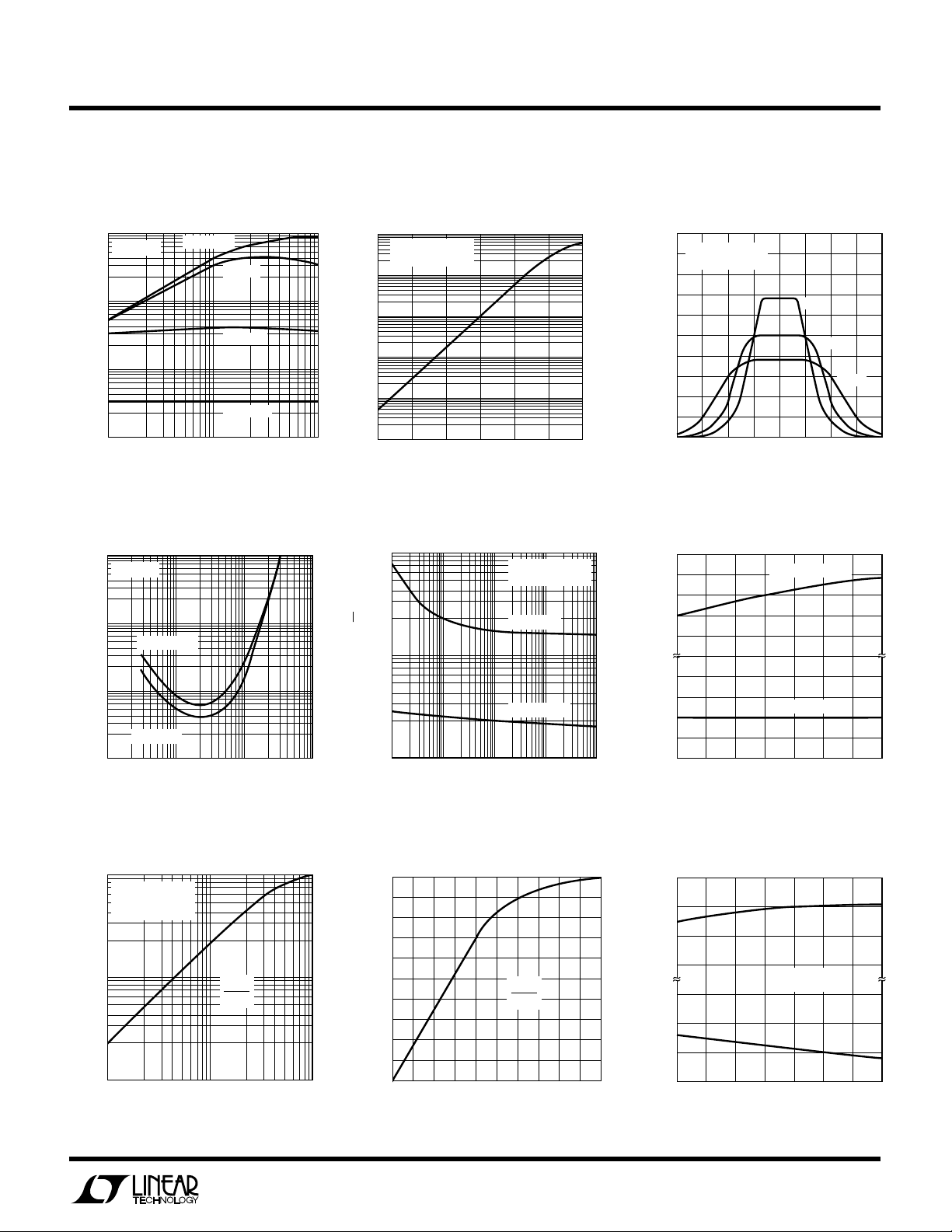
UW
Y
PICA
100
10
1
–3dB BANDWIDTH (MHz)
LPER
F
O
R
AT
CCHARA TERIST
E
C
ICS
Transconductance Amplifier, Pins 1, 2, 3 & 5
Small-Signal Bandwidth vs Small-Signal Transconductance Small-Signal Transconductance
Set Current and Set Current vs Bias Voltage vs DC Input Voltage
VS = ±15V
R1 = 100Ω
R1 = 1k
R1 = 10k
R1 = 100k
100
10
0.1
0.01
TRANSCONDUCTANCE (µA/mV)
1
VS = ±2V TO ±15V
= 25°C
T
A
10000
1000
SET CURRENT (µA)
100
10
1.0
0.1
10
Total Harmonic Distortion vs Spot Output Noise Current vs Input Common-Mode Limit vs
Input Voltage Frequency Temperature
10
VS = ±15V
1
I
= 100µA
SET
0.1
OUTPUT DISTORTION (%)
I
= 1mA
SET
0.01
1
INPUT VOLTAGE (mV
Small-Signal Control Path Small-Signal Control Path Output Saturation Voltage vs
Bandwidth vs Set Current Gain vs Input Voltage Temperature
100
VS = ±2V TO ±15V
= 200mV
V
IN
(PIN 2 TO 3)
10
–3dB BANDWIDTH (MHz)
1
10
100 1000
SET CURRENT (µA)
10 1000
∆I
∆I
100 1000
SET CURRENT (µA)
100
OUT
SET
P–P
LT1228 • TPC01
)
LT1228 • TPC04
LT1228 • TPC07
0.001
1.0 1.1 1.4
0.9 1.2 1.3 1.5
BIAS VOLTAGE, PIN 5 TO 4, (V)
1000
100
SPOT NOISE (pA/√Hz)
1.0
0.9
0.8
0.7
0.6
0.5
0.4
0.3
0.2
CONTROL PATH GAIN (µA/µA)
0.1
10
10
0
100 10k
FREQUENCY (Hz)
40 80 160
0
INPUT VOLTAGE, PIN 2 TO 3, (mVDC)
VS = ±2V TO ±15V
= 25°C
T
A
I
SET
I
SET
1k 100k
∆I
OUT
∆I
SET
120 200
0.1
LT1228 • TPC02
= 1mA
= 100µA
LT1228 • TPC05
LT1228 • TPC08
5
Page 6
LT1228
SUPPLY VOLTAGE (±V)
2
–3dB BANDWIDTH (MHz)
40
100
120
12 16
LT1228 • TPC12
4068101418
0
20
60
140
160
180
80
PEAKING ≤ 0.5dB
PEAKING ≤ 5dB
RF = 750Ω
RF = 1k
RF = 2k
RF = 500Ω
SUPPLY VOLTAGE (±V)
2
–3dB BANDWIDTH (MHz)
40
100
120
12 16
LT1228 • TPC15
4068101418
0
20
60
140
160
180
RF = 500Ω
80
PEAKING ≤ 0.5dB
PEAKING ≤ 5dB
RF = 750Ω
RF = 1k
RF = 2k
RF = 250Ω
SUPPLY VOLTAGE (±V)
2
–3dB BANDWIDTH (MHz)
4
10
12
12 16
LT1228 • TPC18
4068101418
0
2
6
14
16
18
RF = 500Ω
8
RF = 1k
RF = 2k
UW
Y
PICA
8
7
6
5
4
3
2
VOLTAGE GAIN (dB)
1
0
–1
–2
0.1 10 100
22
21
20
19
18
17
16
VOLTAGE GAIN (dB)
15
14
13
12
0.1 10 100
LPER
F
O
R
AT
CCHARA TERIST
E
C
ICS
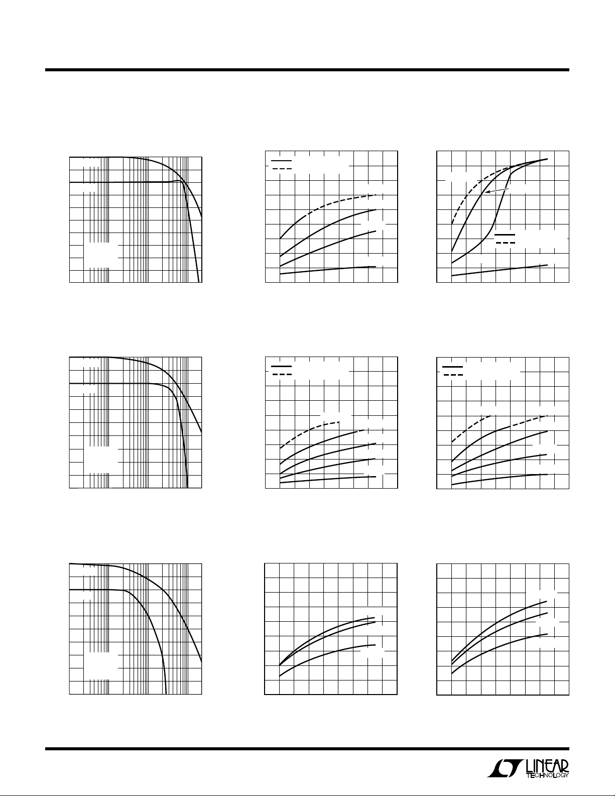
Current Feedback Amplifier, Pins 1, 6, 8
Voltage Gain and Phase vs –3dB Bandwidth vs Supply –3dB Bandwidth vs Supply
Frequency, Gain = 6dB Voltage, Gain = 2, RL = 100Ω Voltage, Gain = 2, RL = 1k
180
160
140
PHASE SHIFT (DEGREES)
120
100
80
60
–3dB BANDWIDTH (MHz)
40
20
0
2
PEAKING ≤ 0.5dB
PEAKING ≤ 5dB
RF = 500Ω
RF = 750Ω
RF = 1k
RF = 2k
4068101418
SUPPLY VOLTAGE (±V)
12 16
LT1228 • TPC11
PHASE
GAIN
VS = ±15V
R
L
= 750Ω
R
F
= 100Ω
1
FREQUENCY (MHz)
0
45
90
135
180
225
LT1228 • TPC10
Voltage Gain and Phase vs –3dB Bandwidth vs Supply –3dB Bandwidth vs Supply
Frequency, Gain = 20dB Voltage, Gain = 10, RL = 100Ω Voltage, Gain = 10, RL = 1kΩ
PHASE
GAIN
VS = ±15V
= 100Ω
R
L
= 750Ω
R
F
1
FREQUENCY (MHz)
0
45
90
135
180
225
LT1228 • TPC13
180
160
PHASE SHIFT (DEGREES)
140
120
100
80
60
–3dB BANDWIDTH (MHz)
40
20
0
2
PEAKING ≤ 0.5dB
PEAKING ≤ 5dB
RF = 250Ω
4068101418
SUPPLY VOLTAGE (±V)
RF = 500Ω
RF = 750Ω
RF = 1k
RF = 2k
12 16
LT1228 • TPC14
Voltage Gain and Phase vs –3dB Bandwidth vs Supply –3dB Bandwidth vs Supply
Frequency, Gain = 40dB Voltage, Gain = 100, RL = 100Ω Voltage, Gain = 100, RL = 1kΩ
42
41
40
39
38
37
36
VOLTAGE GAIN (dB)
35
34
33
32
0.1 10 100
6
PHASE
GAIN
VS = ±15V
= 100Ω
R
L
= 750Ω
R
F
1
FREQUENCY (MHz)
LT1228 • TPC16
0
45
90
PHASE SHIFT (DEGREES)
135
180
225
18
16
14
12
10
–3dB BANDWIDTH (MHz)
8
6
4
2
0
4068101418
2
RF = 500Ω
12 16
SUPPLY VOLTAGE (±V)
RF = 1k
RF = 2k
LT1228 • TPC17
Page 7

UW
TEMPERATURE (°C)
–25
OUTPUT SHORT-CIRCUIT CURRENT (mA)
40
60
100 150
LT1228 • TPC24
0–50 25 50 75 125 175
30
70
50
FREQUENCY (Hz)
OUTPUT IMPEDANCE (Ω)
0.1
100
10k 1M 10M 100M
LT1228 • TPC27
0.001
100k
0.01
10
VS = ±15V
1.0
RF = RG = 2k
RF = RG = 750Ω
Y
PICA
10k
1k
100
CAPACITIVE LOAD (pF)
10
1
+
V
–0.5
–1.0
–1.5
–2.0
2.0
1.5
COMMON-MODE RANGE (V)
1.0
0.5
–
V
–50 25 75 125
LPER
F
O
R
AT
CCHARA TERIST
E
C
ICS
Current Feedback Amplifier, Pins 1, 6, 8
Maximum Capacitive Load vs Total Harmonic Distortion vs 2nd and 3rd Harmonic
Feedback Resistor Frequency Distortion vs Frequency
0.10
VS = ±5V
VS = ±15V
RL = 1k
PEAKING ≤ 5dB
GAIN = 2
023
1
FEEDBACK RESISTOR (kΩ)
LT1228 • TPC19
0.01
TOTAL HARMONIC DISTORTION (%)
0.001
VS = ±15V
= 400Ω
R
L
= RG = 750Ω
R
F
VO = 7V
RMS
VO = 1V
RMS
10 1k 10k 100k
100
FREQUENCY (Hz)
LT1228 • TPC20
–20
VS = ±15V
= 2V
V
O
= 100Ω
R
–30
–40
–50
DISTORTION (dBc)
–60
–70
L
= 750Ω
R
F
= 10dB
A
V
1
P–P
10 100
FREQUENCY (MHz)
Input Common-Mode Limit vs Output Saturation Voltage vs Output Short-Circuit Current vs
Temperature Temperature Temperature
+
V
–0.5
V+ = 2V TO 15V
V– = –2V TO –15V
0
–25 50 100
TEMPERATURE (°C)
LT1228 • TPC22
–1.0
RL = ∞
≤ ±15V
±2V ≤ V
S
1.0
0.5
OUTPUT SATURATION VOLTAGE (V)
–
V
–50 25 75 125
0
–25 50 100
TEMPERATURE (°C)
LT1228 • TPC23
LT1228
2nd
3rd
LT1228 • TPC21
Spot Noise Voltage and Current vs Power Supply Rejection vs Output Impedance vs
Frequency Frequency Frequency
100
–i
10
SPOT NOISE (nV/√Hz OR pA/√Hz)
1
10 1k 10k 100k
n
e
n
+i
100
FREQUENCY (Hz)
n
LT1228 • TPC25
80
VS = ±15V
= 100Ω
R
L
= RG = 750Ω
R
60
40
20
POWER SUPPLY REJECTION (dB)
0
10k 1M 10M 100M
100k
FREQUENCY (Hz)
F
POSITIVE
NEGATIVE
LT1228 • TPC26
7
Page 8

LT1228
UW
LPER
F
O
R
ATYPICA
Settling Time to 10mV vs Settling Time to 1mV vs
Output Step Output Step Supply Current vs Supply Voltage
10
NONINVERTING
8
6
4
2
0
–2
OUTPUT STEP (V)
–4
–6
–8
NONINVERTING
–10
200 40 80 100
SETTLING TIME (ns)
INVERTING
V
S
R
F
INVERTING
60
= ±15V
= RG = 1k
LT1228 • TPC28
CCHARA TERIST
E
C
10
NONINVERTING
8
6
4
2
0
–2
OUTPUT STEP (V)
–4
–6
–8
–10
NONINVERTING
40 8 16 20
ICS
INVERTING
V
R
INVERTING
12
SETTLING TIME (µs)
Current Feedback Amplifier, Pins 1, 6 & 8
10
9
8
7
= ±15V
S
= RG = 1k
F
LT1228 • TPC29
6
5
4
3
SUPPLY CURRENT (mA)
2
1
0
125°C
175°C
40816
2 6 10 14 18
SUPPLY VOLTAGE (±V)
–55°C
25°C
12
LT1228 • TPC30
W
SPL
I
IIFED S
I
SET
W
A
E
CH
5
C
TI
+
V
7
BIAS
–IN+IN
23
I
OUT
1
8
GAIN V
6
OUT
–
V
4
LT1228 • TA03
8
Page 9

LT1228
PPLICATI
A
U
O
S
I FOR ATIO
WU
U
The LT1228 contains two amplifiers, a transconductance
amplifier (voltage-to-current) and a current feedback amplifier (voltage-to-voltage). The gain of the transconductance amplifier is proportional to the current that is externally programmed into pin 5. Both amplifiers are designed
to operate on almost any available supply voltage from 4V
(±2V) to 30V (±15V). The output of the transconductance
amplifier is connected to the noninverting input of the
current feedback amplifier so that both fit into an eight pin
package.
TRANSCONDUCTANCE AMPLIFIER
The LT1228 transconductance amplifier has a high impedance differential input (pins 2 and 3) and a current source
output (pin 1) with wide output voltage compliance. The
voltage to current gain or transconductance (gm) is set by
the current that flows into pin 5, I
. The voltage at pin 5
SET
is two forward biased diode drops above the negative
supply, pin 4. Therefore the voltage at pin 5 (with
respect to V–) is about 1.2V and changes with the log of
the set current (120mV/decade), see the characteristic
curves. The temperature coefficient of this voltage is
about –4mV/°C (–3300ppm/°C) and the temperature coefficient of the logging characteristic is 3300ppm/°C. It is
important that the current into pin 5 be limited to less than
15mA. THE LT1228 WILL BE DESTROYED IF PIN 5 IS
SHORTED TO GROUND OR TO THE POSITIVE SUPPLY. A
limiting resistor (2k or so) should be used to prevent more
than 15mA from flowing into pin 5.
The small-signal transconductance (gm) is equal to ten
times the value of I
(in mA/mV) and this relationship
SET
holds over many decades of set current (see the characteristic curves). The transconductance is inversely proportional to absolute temperature (–3300ppm/°C). The input
stage of the transconductance amplifier has been designed to operate with much larger signals than is possible
with an ordinary diff-amp. The transconductance of the
input stage varies much less than 1% for differential input
signals over a ±30 mV range (see the characteristic curve
Small-Signal Transconductance vs DC Input Voltage).
Resistance Controlled Gain
If the set current is to be set or varied with a resistor or
potentiometer it is possible to use the negative temperature coefficient at pin 5 (with respect to pin 4) to compensate for the negative temperature coefficient of the transconductance. The easiest way is to use an LT1004-2.5, a 2.5V
reference diode, as shown below:
Temperature Compensation of gm with a 2.5V Reference
R
I
SET
g
m
4
5
R
LT1004-2.5
–
V
I
SET
2.5V
2E
g
LT1228 • TA04
V
be
V
be
The current flowing into pin 5 has a positive temperature
coefficient that cancels the negative coefficient of the
transconductance. The following derivation shows why a
2.5V reference results in zero gain change with temperature:
qkTI
Since g
and V E
c n Ic A
()
=× =×
m
==
be g
0 001 3 100
., , µ
===
SET
387
.
akT
where a In
–.
q
10
I
SET
n
cT
19 4 27
š
Ic
at C
Eg is about 1.25V so the 2.5V reference is 2Eg. Solving
the loop for the set current gives:
I
SET
=
EE
22
––
gg
R
akT
q
or I
SET
=
akT
2
Rq
9
Page 10

LT1228
PPLICATI
A
U
O
S
I FOR ATIO
WU
U
Substituting into the equation for transconductance gives:
g
a
==
m
19410.
RR
The temperature variation in the term “a” can be ignored
since it is much less than that of the term “T” in the
equation for Vbe. Using a 2.5V source this way will maintain the gain constant within 1% over the full temperature
range of –55°C to 125°C. If the 2.5V source is off by 10%,
the gain will vary only about ±6% over the same temperature range.
We can also temperature compensate the transconductance without using a 2.5V reference if the negative power
supply is regulated. A Thevenin equivalent of 2.5V is
generated from two resistors to replace the reference. The
two resistors also determine the maximum set current,
approximately 1.1V/RTH. By rearranging the Thevenin
equations to solve for R4 and R6 we get the following
equations in terms of RTH and the negative supply, VEE.
R
=
R
4
TH
25
–
1
andR
.
V
V
EE
6
RV
=
TH EE
.
25
V
is two diode drops above the negative supply, a single
resistor from the control voltage source to pin 5 will suffice
in many applications. The control voltage is referenced to
the negative supply and has an offset of about 900mV. The
conversion will be monotonic, but the linearity is determined by the change in the voltage at pin 5 (120mV per
decade of current). The characteristic is very repeatable
since the voltage at pin 5 will vary less than ±5% from part
to part. The voltage at pin 5 also has a negative temperature coefficient as described in the previous section. When
the gain of several LT1228s are to be varied together, the
current can be split equally by using equal value resistors
to each pin 5.
For more accurate (and linear) control, a voltage-tocurrent converter circuit using one op amp can be used.
The following circuit has several advantages. The input no
longer has to be referenced to the negative supply and the
input can be either polarity (or differential). This circuit
works on both single and split supplies since the input
voltage and the pin 5 voltage are independent of each
other. The temperature coefficient of the output current is
set by R5.
Temperature Compensation of gm with a Thevenin Voltage
R6
6.19kΩ
R4
1.24kΩ
1.03k
g
m
4
5
R'
I
SET
–15V
VTH = 2.5V
R'
I
SET
V
be
V
be
LT1228 • TA05
Voltage Controlled Gain
To use a voltage to control the gain of the transconductance amplifier requires converting the voltage into a
current that flows into pin 5. Because the voltage at pin 5
R3
1M
R1
1M
V1
R2
1M
V2
R1 = R2
R3 = R4
(V1 – V2)R5R3
= × = 1mA/V
I
OUT
R1
+
–
LT1006
50pF
1M
R4
R5
1k
I
OUT
TO PIN 5
OF LT1228
LT1228 • TA19
Digital control of the transconductance amplifier gain is
done by converting the output of a DAC to a current flowing
into pin 5. Unfortunately most current output DACs
sink rather than source current and do not have output
10
Page 11

LT1228
U
O
PPLICATI
A
compliance compatible with pin 5 of the LT1228. Therefore, the easiest way to digitally control the set current is
to use a voltage output DAC and a voltage-to-current
circuit. The previous voltage-to-current converter will take
the output of any voltage output DAC and drive pin 5 with
a proportional current. The R, 2R CMOS multiplying DACs
operating in the voltage switching mode work well on both
single and split supplies with the above circuit.
Logarithmic control is often easier to use than linear
control. A simple circuit that doubles the set current for
each additional volt of input is shown in the voltage
controlled state variable filter application near the end of
this data sheet.
Transconductance Amplifier Frequency Response
The bandwidth of the transconductance amplifier is a
function of the set current as shown in the characteristic
curves. At set currents below 100µA, the bandwidth is
approximately:
–3dB bandwidth = 3 × 10
The peak bandwidth is about 80MHz at 500µA. When a
resistor is used to convert the output current to a voltage,
the capacitance at the output forms a pole with the
resistor. The best case output capacitance is about 5pF
with ±15V supplies and 6pF with ±5V supplies. You must
add any PC board or socket capacitance to these values to
get the total output capacitance. When using a 1k resistor
at the output of the transconductance amp, the output
capacitance limits the bandwidth to about 25MHz.
The output slew rate of the transconductance amplifier is
the set current divided by the output capacitance, which is
6pF plus board and socket capacitance. For example with
the set current at 1mA, the slew rate would be over
100V/µs.
S
I FOR ATIO
11
I
SET
WU
U
Transconductance Amp Small-Signal Response
I
= 500µA, R1 = 50Ω
SET
CURRENT FEEDBACK AMPLIFIER
The LT1228 current feedback amplifier has very high
noninverting input impedance and is therefore an excellent buffer for the output of the transconductance amplifier. The noninverting input is at pin 1, the inverting input
at pin 8 and the output at pin 6. The current feedback
amplifier maintains its wide bandwidth for almost all
voltage gains making it easy to interface the output levels
of the transconductance amplifier to other circuitry. The
current feedback amplifier is designed to drive low impedance loads such as cables with excellent linearity at high
frequencies.
Feedback Resistor Selection
The small-signal bandwidth of the LT1228 current feedback amplifier is set by the external feedback resistors and
the internal junction capacitors. As a result, the bandwidth
is a function of the supply voltage, the value of the
feedback resistor, the closed-loop gain and load resistor.
The characteristic curves of bandwidth versus supply
voltage are done with a heavy load (100Ω) and a light load
(1k) to show the effect of loading. These graphs also show
11
Page 12

LT1228
PPLICATI
A
U
O
S
I FOR ATIO
WU
U
the family of curves that result from various values of the
feedback resistor. These curves use a solid line when the
response has less than 0.5dB of peaking and a dashed line
for the response with 0.5dB to 5dB of peaking. The curves
stop where the response has more than 5dB of peaking.
Current Feedback Amp Small-Signal Response
VS = ±15V, RF = RG = 750Ω, RL = 100Ω
Capacitance on the Inverting Input
Current feedback amplifiers want resistive feedback from
the output to the inverting input for stable operation. Take
care to minimize the stray capacitance between the output
and the inverting input. Capacitance on the inverting input
to ground will cause peaking in the frequency response
(and overshoot in the transient response), but it does not
degrade the stability of the amplifier. The amount of
capacitance that is necessary to cause peaking is a function of the closed-loop gain taken. The higher the gain, the
more capacitance is required to cause peaking. For example, in a gain of 100 application, the bandwidth can be
increased from 10MHz to 17MHz by adding a 2200pF
capacitor, as shown below. CG must have very low series
resistance, such as silver mica.
1
V
IN
+
CFA
8
–
R
510Ω
6
F
V
OUT
At a gain of two, on ± 15V supplies with a 750Ω feedback
resistor, the bandwidth into a light load is over 160MHz
without peaking, but into a heavy load the bandwidth
reduces to 100MHz. The loading has so much effect
because there is a mild resonance in the output stage that
enhances the bandwidth at light loads but has its Q
reduced by the heavy load. This enhancement is only
useful at low gain settings, at a gain of ten it does not boost
the bandwidth. At unity gain, the enhancement is so
effective the value of the feedback resistor has very little
effect on the bandwidth. At very high closed-loop gains,
the bandwidth is limited by the gain-bandwidth product of
about 1GHz. The curves show that the bandwidth at a
closed-loop gain of 100 is 10MHz, only one tenth what it
is at a gain of two.
C
Boosting Bandwidth of High Gain Amplifier
with Capacitance On Inverting Input
49
46
43
40
37
34
GAIN (dB)
31
28
25
22
19
RG
G
5.1Ω
LT1228 • TA08
CG = 4700pF
C
= 2200pF
G
C
= 0
G
1
10 100
FREQUENCY (MHz)
LT1228 • TA09
12
Page 13

LT1228
U
O
PPLICATI
A
Capacitive Loads
The LT1228 current feedback amplifier can drive capacitive loads directly when the proper value of feedback
resistor is used. The graph of Maximum Capacitive Load
vs Feedback Resistor should be used to select the appropriate value. The value shown is for 5dB peaking when
driving a 1k load, at a gain of 2. This is a worst case
condition, the amplifier is more stable at higher gains, and
driving heavier loads. Alternatively, a small resistor (10Ω
to 20Ω) can be put in series with the output to isolate the
capacitive load from the amplifier output. This has the
advantage that the amplifier bandwidth is only reduced
when the capacitive load is present and the disadvantage
that the gain is a function of the load resistance.
Slew Rate
The slew rate of the current feedback amplifier is not
independent of the amplifier gain configuration the way it
is in a traditional op amp. This is because the input stage
and the output stage both have slew rate limitations. The
input stage of the LT1228 current feedback amplifier slews
at about 100V/µs before it becomes nonlinear. Faster
input signals will turn on the normally reverse biased
emitters on the input transistors and enhance the slew rate
significantly. This enhanced slew rate can be as much as
3500V/µs!
Current Feedback Amp Large-Signal Response
VS = ±15V, RF = RG = 750Ω Slew Rate Enhanced
S
I FOR ATIO
WU
U
The output slew rate is set by the value of the feedback
resistors and the internal capacitance. At a gain of ten with
a 1k feedback resistor and ±15V supplies, the output slew
rate is typically 500V/µs and –850V/µs. There is no input
stage enhancement because of the high gain. Larger
feedback resistors will reduce the slew rate as will lower
supply voltages, similar to the way the bandwidth is
reduced.
Current Feedback Amp Large-Signal Response
VS = ±15V, RF = 1k, RG = 110Ω, RL = 400Ω
Settling Time
The characteristic curves show that the LT1228 current
feedback amplifier settles to within 10mV of final value in
40ns to 55ns for any output step less than 10V. The curve
of settling to 1mV of final value shows that there is a slower
thermal contribution up to 20µs. The thermal settling
component comes from the output and the input stage.
The output contributes just under 1mV/V of output change
and the input contributes 300µV/V of input change.
Fortunately the input thermal tends to cancel the output
thermal. For this reason the noninverting gain of two
configuration settles faster than the inverting gain of one.
13
Page 14

LT1228
U
O
PPLICATI
A
Power Supplies
The LT1228 amplifiers will operate from single or split
supplies from ±2V (4V total) to ± 18V (36V total). It is not
necessary to use equal value split supplies, however the
offset voltage and inverting input bias current of the
current feedback amplifier will degrade. The offset voltage
changes about 350µV/V of supply mismatch, the inverting
bias current changes about 2.5µA/V of supply mismatch.
Power Dissipation
The worst case amplifier power dissipation is the total of
the quiescent current times the total power supply voltage
plus the power in the IC due to the load. The quiescent
supply current of the LT1228 transconductance amplifier
is equal to 3.5 times the set current at all temperatures. The
quiescent supply current of the LT1228 current feedback
amplifier has a strong negative temperature coefficient
and at 150°C is less than 7mA, typically only 4.5mA. The
power in the IC due to the load is a function of the output
voltage, the supply voltage and load resistance. The worst
case occurs when the output voltage is at half supply, if it
can go that far, or its maximum value if it cannot reach half
supply.
S
I FOR ATIO
WU
U
For example, let’s calculate the worst case power dissipation in a variable gain video cable driver operating on ±12V
supplies that delivers a maximum of 2V into 150Ω. The
maximum set current is 1mA.
V
235
PVI I VV
=+
D S SMAX SET S OMAX
P V mA mA V V
D
The total power dissipation times the thermal resistance of
the package gives the temperature rise of the die above
ambient. The above example in SO-8 surface mount
package (thermal resistance is 150°C/W) gives:
Temperature Rise = PDθJA = 0.385W × 150°C/W
Therefore the maximum junction temperature is 70°C
+57.75°C or 127.75°C, well under the absolute maximum
junction temperature for plastic packages of 150°C.
()
=× × + ×
212 7 351 12 2
=+=
0 252 0 133 0 385
...
.–
+
()
.–
[]
()
W
= 57.75°C
OMAX
R
L
2
+
()
V
150
Ω
U
O
PPLICATITYPICAL
Basic Gain Control
The basic gain controlled amplifier is shown on the front
page of the data sheet. The gain is directly proportional to
the set current. The signal passes through three stages
from the input to the output.
First the input signal is attenuated to match the dynamic
range of the transconductance amplifier. The attenuator
should reduce the signal down to less than 100mV peak.
The characteristic curves can be used to estimate how
much distortion there will be at maximum input signal. For
single ended inputs eliminate R2A or R3A.
The signal is then amplified by the transconductance
amplifier (gm) and referred to ground. The voltage gain of
the transconductance amplifier is:
SA
gR I R
×=× ×110 1
m SET
Lastly the signal is buffered and amplified by the current
feedback amplifier (CFA). The voltage gain of the current
feedback amplifier is:
R
F
1+
R
G
The overall gain of the gain controlled amplifier is the
product of all three stages:
A
=
V SET
RRA
33
More than one output can be summed into R1 because the
output of the transconductance amplifier is a current. This
is the simplest way to make a video mixer.
R
3
+
×× ××+
IR
10 1 1
R
F
R
G
14
Page 15

LT1228
U
O
PPLICATITYPICAL
SA
Video Fader
1k
V
IN1
100Ω
1k
V
IN2
100Ω
1k
–5V
1k
3
+
g
m
2
–
3
+
g
m
2
–
1
5
5.1k10k
10k
5.1k10k
5
1
V
= ±5V
S
+
LT1223
–
CFA
LT1228 • TA12
V
OUT
The video fader uses the transconductance amplifiers
from two LT1228s in the feedback loop of another current
feedback amplifier, the LT1223. The amount of signal
from each input at the output is set by the ratio of the
set currents of the two LT1228s, not by their absolute
value. The bandwidth of the current feedback amplifier
is inversely proportional to the set current in this
configuration. Therefore, the set currents remain high
over most of the pot’s range, keeping the bandwidth over
15MHz even when the signal is attenuated 20dB. The pot
is set up to completely turn off one LT1228 at each end of
the rotation.
Video DC Restore (Clamp) Circuit
NOT NECESSARY IF THE SOURCE RESISTANCE IS LESS THAN 50Ω
1000pF
LOGIC
INPUT
RESTORE
200Ω
3
2
2N3906
+
V
7
+
g
m
–
5
4
10k
–
V
5V
3k
3k
VIDEO
INPUT
0.01µF
1
+
CFA
8
–
R
G
6
V
OUT
R
F
LT1228 • TA13
The video restore (clamp) circuit restores the black level of
the composite video to zero volts at the beginning of every
line. This is necessary because AC coupled video changes
DC level as a function of the average brightness of the
picture. DC restoration also rejects low frequency noise
such as hum.
The circuit has two inputs: composite video and a logic
signal. The logic signal is high except during the back
porch time right after the horizontal sync pulse. While the
logic is high, the PNP is off and I
is zero. With I
SET
SET
equal
to zero the feedback to pin 2 has no affect. The video input
drives the noninverting input of the current feedback
amplifier whose gain is set by RF and RG. When the logic
signal is low, the PNP turns on and I
goes to about 1mA.
SET
Then the transconductance amplifier charges the capacitor to force the output to match the voltage at pin 3, in this
case zero volts.
This circuit can be modified so that the video is DC coupled
by operating the amplifier in an inverting configuration.
Just ground the video input shown and connect RG to the
video input instead of to ground.
15
Page 16

LT1228
CA
U
O
PPLICATITYPI
L
SA
Single Supply Wien Bridge Oscillator
100Ω
2N3906
+
V
10kΩ
10kΩ
10µF
6V TO 30V
+
V
7
3
+
g
m
2
–
4
+
f = 1MHz
= 6dBm (450mV
V
O
2nd HARMONIC = –38dBc
3rd HARMONIC = –54 dBc
FOR 5V OPERATION SHORT OUT 100Ω RESISTOR
160Ω
1000pF 1000pF
RMS
)
470Ω
5
1.8k
+
10µF
1
+
8
–
R
G
20Ω
+
10µF
CFA
680Ω
R
F
160Ω
3 at resonance; therefore the attenuation of the 1.8k resistor and the transconductance amplifier must be about 11,
resulting in a set current of about 600µA at oscillation. At
start-up there is no set current and therefore no attenuation
for a net gain of about 11 around the loop. As the output
oscillation builds up it turns on the PNP transistor which
generates the set current to regulate the output voltage.
0.1µF
6
51Ω
50Ω
LT1228 • TA14
12MHz Negative Resistance LC Oscillator
+
V
9.1k
V
O
4.7µH
3
1k
2
30pF
7
+
g
m
–
4
–
V
4.3k
2N3904
1
+
5
8
–
330Ω
10k
CFA
50Ω
2N3906
V
O
51Ω
6
1k
0.1µF
750Ω
In this application the LT1228 is biased for operation from
a single supply. An artificial signal ground at half supply
voltage is generated with two 10k resistors and bypassed
with a capacitor. A capacitor is used in series with RG to set
the DC gain of the current feedback amplifier to unity.
The transconductance amplifier is used as a variable resistor to control gain. A variable resistor is formed by driving
the inverting input and connecting the output back to it. The
equivalent resistor value is the inverse of the gm. This
works with the 1.8k resistor to make a variable attenuator.
The 1MHz oscillation frequency is set by the Wien bridge
network made up of two 1000pF capacitors and two 160Ω
resistors.
For clean sine wave oscillation, the circuit needs a net gain
of one around the loop. The current feedback amplifier has
a gain of 34 to keep the voltage at the transconductance
amplifier input low. The Wien bridge has an attenuation of
–
VO = 10dB
= ±5V ALL HARMONICS 40dB DOWN
AT V
S
= ±12V ALL HARMONICS 50dB DOWN
AT V
S
V
LT1228 • TA15
This oscillator uses the transconductance amplifier as a
negative resistor to cause oscillation. A negative resistor
results when the positive input of the transconductance
amplifier is driven and the output is returned to it. In this
example a voltage divider is used to lower the signal level at
the positive input for less distortion. The negative resistor
will not DC bias correctly unless the output of the transconductance amplifier drives a very low resistance. Here it sees
an inductor to ground so the gain at DC is zero. The
oscillator needs negative resistance to start and that is
provided by the 4.3k resistor to pin 5. As the output level
rises it turns on the PNP transistor and in turn the NPN
which steals current from the transconductance amplifier
bias input.
16
Page 17

Filters
LT1228
U
O
V
LOWPASS
INPUT
HIGHPASS
INPUT
SA
Single Pole Low/High/Allpass Filter
R3A
1k
IN
120Ω
V
IN
3
+
g
R3
m
2
–
330pF
5
I
SET
RG
1k
1
R2A
1k
+
6
CFA
8
–
R
F
1k
V
OUT
C
PPLICATITYPICAL
R2
120Ω
102πI
f
= × × ×
C
fC = 109 I
Allpass Filter Phase Response
0
–45
–90
–135
PHASE SHIFT (DEGREES)
100µA SET CURRENT
–180
10k
1mA SET CURRENT
100k 1M 10M
FREQUENCY (Hz)
Using the variable transconductance of the LT1228 to
make variable filters is easy and predictable. The most
straight forward way is to make an integrator by putting a
capacitor at the output of the transconductance amp and
buffering it with the current feedback amplifier. Because
the input bias current of the current feedback amplifier
must be supplied by the transconductance amplifier, the
set current should not be operated below 10µA. This limits
the filters to about a 100:1 tuning range.
The Single Pole circuit realizes a single pole filter with a
corner frequency (fC) proportional to the set current. The
CRF + 1
SET
R
FOR THE VALUES SHOWN
SET
G
LT1228 • TA17
R2
R2 + R2A
LT1228 • TA16
values shown give a 100kHz corner frequency for 100µA
set current. The circuit has two inputs, a lowpass filter
input and a highpass filter input. To make a lowpass filter,
ground the highpass input and drive the lowpass input.
Conversely for a highpass filter, ground the lowpass input
and drive the highpass input. If both inputs are driven, the
result is an allpass filter or phase shifter. The allpass has
flat amplitude response and 0° phase shift at low frequencies, going to –180° at high frequencies. The allpass filter
has –90° phase shift at the corner frequency.
17
Page 18

LT1228
U
O
PPLICATITYPICAL
Voltage Controlled State Variable Filter
SA
10k
V
C
180Ω
3.3k
V
IN
100Ω
100Ω
f
= 100kHz AT VC = 0V
O
= 200kHz AT VC = 1V
f
O
= 400kHz AT VC = 2V
f
O
= 800kHz AT VC = 3V
f
O
= 1.6MHz AT VC = 4V
f
O
100Ω
–5V
3
2
2N3906
51k
5V
+
g
–
3
+
2
–
7
m
–5V
5V
1k
+
LT1006
–
100pF
3k
3k
5
4
18pF
3.3k
3.3k
7
5
g
m
4
18pF
–5V
3.3k
1
+
CFA
8
–
1
+
CFA
8
–
6
BANDPASS
OUTPUT
1k
LOWPASS
6
OUTPUT
1k
LT1228 • TA18
The state variable filter has both lowpass and bandpass
outputs. Each LT1228 is configured as a variable integrator whose frequency is set by the attenuators, the capacitors and the set current. Because the integrators have both
positive and negative inputs, the additional op amp normally required is not needed. The input attenuators set the
circuit up to handle 3V
signals.
P–P
The set current is generated with a simple circuit that gives
logarithmic voltage to current control. The two PNP transistors should be a matched pair in the same package for
18
best accuracy. If discrete transistors are used, the 51k
resistor should be trimmed to give proper frequency
response with VC equal zero. The circuit generates 100µA
for VC equal zero volts and doubles the current for every
additional volt. The two 3k resistors divide the current
between the two LT1228s. Therefore the set current of
each amplifier goes from 50µA to 800µA for a control
voltage of 0V to 4V. The resulting filter is at 100kHz for V
C
equal zero, and changes it one octave/V of control input.
Page 19

0.6V
RMS to
PPLICATITYPICAL
RF INPUT
1.3V
25MHz
RMS
LT1228
U
O
SA
RF AGC Amplifier (Leveling Loop)
15V
10k
100
3
Ω
7
+
g
m
2
–
5
10k
300
0.01µF
1
+
Ω
8
10k
CFA
–
4
–15V
4pF
470
10
Ω
Ω
OUTPUT
2V
0.01µF
10k
P–P
15V
–
A3
LT1006
+
–15V
10k
100k
AMPLITUDE
ADJUST
COUPLE THERMALLY
Inverting Amplifier with DC Output Less Than 5mV
+
V
2
3
VS = ±5V, R5 = 3.6k
= ±15V, R5 = 13.6k
V
S
MUST BE LESS THAN
V
OUT
200mV
P–P
BW = 30Hz TO 20MHz
7
–
g
m
+
4
–
V
FOR LOW OUTPUT OFFSET
+
5
R5
1
100µF
8
R
G
1k
V
IN
INCLUDES DC
+
CFA
6
–
R
F
1k
Amplitude Modulator
1N4148’s
LT1228 • TA21
4.7k
–15V
LT1004
1.2V
LT1228 • TA20
V
O
5V
4.7µF
+
3
4.7µF
2
+
CARRIER
INPUT
30mV
Information furnished by Linear Technology Corporation is believed to be accurate and reliable.
However, no responsibility is assumed for its use. Linear Technology Corporation makes no representation that the interconnection of its circuits as described herein will not infringe on existing patent rights.
+
g
m
–
4
–5V
MODULATION
INPUT ≤ 8V
7
1
+
5
10k
1k
P–P
8
R
G
750Ω
CFA
–
R
F
750Ω
6
V
OUT
0dBm(230mV) AT
MODULATION = 0V
LT1228 • TA22
19
Page 20

LT1228
J8 0293
0.014 – 0.026
(0.360 – 0.660)
0.200
(5.080)
MAX
0.015 – 0.060
(0.381 – 1.524)
0.125
3.175
MIN
0.100 ± 0.010
(2.540 ± 0.254)
0.300 BSC
(0.762 BSC)
0.008 – 0.018
(0.203 – 0.457)
0° – 15°
0.385 ± 0.025
(9.779 ± 0.635)
0.005
(0.127)
MIN
0.405
(10.287)
MAX
0.220 – 0.310
(5.588 – 7.874)
12
3
4
87
65
0.025
(0.635)
RAD TYP
0.045 – 0.068
(1.143 – 1.727)
FULL LEAD
OPTION
0.023 – 0.045
(0.584 – 1.143)
HALF LEAD
OPTION
CORNER LEADS OPTION
(4 PLCS)
0.045 – 0.068
(1.143 – 1.727)
NOTE: LEAD DIMENSIONS APPLY TO SOLDER DIP OR TIN PLATE LEADS.
PACKAGEDESCRIPTI
U
O
Dimensions in inches (millimeters) unless otherwise noted.
J8 Package
8-Lead Ceramic DIP
0.008 – 0.010
(0.203 – 0.254)
20
N8 Package
8-Lead Plastic DIP
0.300 – 0.320
(7.620 – 8.128)
0.065
(1.651)
0.009 – 0.015
(0.229 – 0.381)
+0.025
0.325
–0.015
+0.635
8.255
()
–0.381
*THESE DIMENSIONS DO NOT INCLUDE MOLD FLASH OR PROTRUSIONS.
MOLD FLASH OR PROTURSIONS SHALL NOT EXCEED 0.010 INCH (0.254mm).
TYP
0.045 ± 0.015
(1.143 ± 0.381)
(2.540 ± 0.254)
0.045 – 0.065
(1.143 – 1.651)
0.100 ± 0.010
S8 Package
8-Lead Plastic SOIC
0.010 – 0.020
(0.254 – 0.508)
*THESE DIMENSIONS DO NOT INCLUDE MOLD FLASH OR PROTRUSIONS.
MOLD FLASH OR PROTRUSIONS SHALL NOT EXCEED 0.006 INCH (0.15mm).
× 45°
0.016 – 0.050
0.406 – 1.270
0.053 – 0.069
(1.346 – 1.752)
0°– 8° TYP
0.014 – 0.019
(0.355 – 0.483)
Linear Technology Corporation
1630 McCarthy Blvd., Milpitas, CA 95035-7487
(408) 432-1900
●
FAX
: (408) 434-0507
●
TELEX
: 499-3977
0.130 ± 0.005
(3.302 ± 0.127)
0.125
(3.175)
MIN
0.018 ± 0.003
(0.457 ± 0.076)
0.004 – 0.010
(0.101 – 0.254)
0.050
(1.270)
BSC
0.020
(0.508)
MIN
N8 0594
0.228 – 0.244
(5.791 – 6.197)
0.250 ± 0.010*
(6.350 ± 0.254)
0.400*
(10.160)
MAX
876
5
12
0.189 – 0.197*
(4.801 – 5.004)
7
8
1
LINEAR TECHNOLOGY CORPORATION 1994
6
3
2
LT/GP 0694 5K REV A • PRINTED IN USA
3
5
4
4
0.150 – 0.157*
(3.810 – 3.988)
SO8 0294
 Loading...