

Page 1
LT1227
140MHz Video Current
Feedback Amplifier
EATU
F
■
140MHz Bandwidth: AV = 2, R
■
1100V/µs Slew Rate
■
Low Cost
■
30mA Output Drive Current
■
0.01% Differential Gain
■
0.01° Differential Phase
■
High Input Impedance: 14MΩ, 3pF
■
Wide Supply Range: ±2V to ±15V
■
Shutdown Mode: IS < 250µA
■
Low Supply Current: IS = 10mA
■
Inputs Common Mode to Within 1.5V of Supplies
■
Outputs Swing Within 0.8V of Supplies
PPLICATI
A
■
Video Amplifiers
■
Cable Drivers
■
RGB Amplifiers
■
Test Equipment Amplifiers
■
50Ω Buffers for Driving Mixers
RE
S
O
U
S
= 150Ω
L
DUESCRIPTIO
The LT1227 is a current feedback amplifier with wide
bandwidth and excellent video characteristics. The low
differential gain and phase, wide bandwidth, and 30mA
output drive current make the LT1227 well suited to drive
cables in video systems.
A shutdown feature switches the device into a high impedance, low current mode, allowing multiple devices to be
connected in parallel and selected. Input to output isolation in shutdown is 70dB at 10MHz for input amplitudes up
to 10V
or open drain logic and takes only 4µ s to enable or disable.
The LT1227 comes in the industry standard pinout and
can upgrade the performance of many older products. For
a dual or quad version, see the LT1229/1230 data sheet.
The LT1227 is manufactured on Linear Technology’s
proprietary complementary bipolar process.
. The shutdown pin interfaces to open collector
P-P
U
O
A
PPLICATITYPICAL
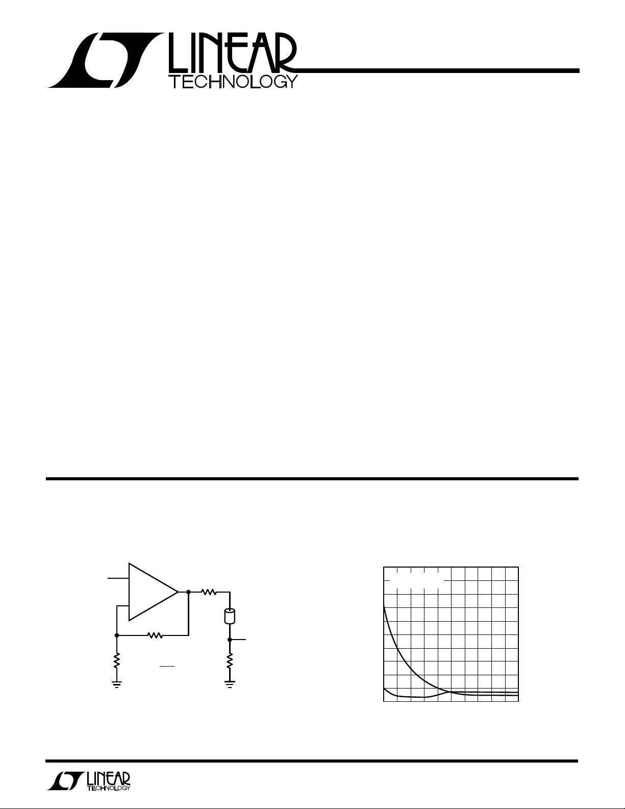
Video Cable Driver Differential Gain and Phase
vs Supply Voltage
0.20
V
IN
+
LT1227
–
RF
1k
RG
1k
V
OUT
V
IN
= 1
75Ω
75Ω
CABLE
V
OUT
75Ω
1227 TA01
NTSC COMPOSITE
f = 3.58MHz
0.16
0.12
0.08
DIFFERENTIAL PHASE (DEG)
0.04
0
5
∆φ
∆G
7
9
SUPPLY VOLTAGE (±V)
11
13
LT1227 • TA02
0.20
0.16
DIFFERENTIAL GAIN (%)
0.12
0.08
0.04
0
15
1
Page 2
LT1227
A
W
O
LUTEXI T
S
A
WUW
ARB
U
G
I
S
Supply Voltage ..................................................... ±18V
Input Current ...................................................... ±15mA
Output Short Circuit Duration (Note 1) ........ Continuous
Operating Temperature Range
LT1227C.................................................. 0°C to 70°C
LT1227M ......................................... – 55°C to 125°C
Storage Temperature Range ................. –65°C to 150°C
Junction Temperature
Plastic Package ................................................ 150°C
Ceramic Package ............................................. 175°C
Lead Temperature (Soldering, 10 sec.)................ 300°C
/
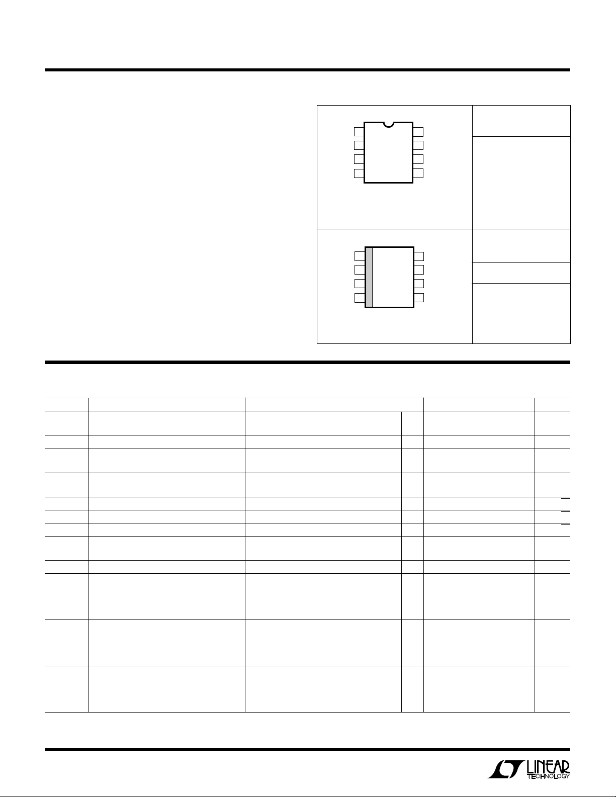
TOP VIEW
= 175°C, θ
150°C, θ
TOP VIEW
S8 PACKAGE
150°C, θ
O
RDER I FOR ATIO
8
SHUTDOWN
+
7
V
6
OUT
NULL
N8 PACKAGE
8-LEAD PLASTIC DIP
100°C/W (J)
JA =
100°C/W (N)
JA =
8
SHUTDOWN
+
7
V
6
OUT
NULL
150°C/W
JA =
PACKAGE
1
NULL
2
–IN
3
+IN
–
V
45
J8 PACKAGE
8-LEAD CERAMIC DIP
T
JMAX
T
JMAX =
1
NULL
2
–IN
3
+IN
–
V
45
8-LEAD PLASTIC SO
T
JMAX =
Consult factory for Industrial grade parts.
WU
ORDER PART
NUMBER
LT1227MJ8
LT1227CN8
LT1227CS8
S8 PART MARKING
1227
U
LECTRICAL C CHARA TERIST
E
SYMBOL PARAMETER CONDITIONS MIN TYP MAX UNITS
V
OS
+ Noninverting Input Current T
I
IN
– Inverting Input Current T
I
IN
e
n
+i
n
–i
n
R
IN
C
IN
CMRR Common-Mode Rejection Ratio VS = ±15V, VCM = ±13V, TA = 25°C5562 dB
Input Offset Voltage TA = 25°C ±3 ±10 mV
Input Offset Voltage Drift ● 10 µV/°C
Input Noise Voltage Density f = 1kHz, RF = 1k, RG = 10Ω, RS = 0Ω 3.2 nV/√Hz
Noninverting Input Noise Current Density f = 1kHz 1.7 pA/√Hz
Inverting Input Noise Current Density f = 1kHz 32 pA/√Hz
Input Resistance VIN = ±13V, VS = ±15V ● 1.5 14 MΩ
Input Capacitance 3pF
Input Voltage Range VS = ±15V, TA = 25°C ±13 ±13.5 V
Inverting Input Current V
Common-Mode Rejection VS = ±15V, VCM = ±12V ● 10 µA/V
ICS
VCM = 0, ±5V ≤ VS ≤ ±15V, pulse tested, unless otherwise noted.
● ±15 mV
= 25°C ±0.3 ±3 µA
A
= 25°C ±10 ±60 µA
A
VIN = ±3V, VS = ±5V ● 1.5 11 MΩ
= ±5V, TA = 25°C ±3 ±3.5 V
V
S
= ±15V, VCM = ±12V ● 55 dB
V
S
= ±5V, VCM = ±3V, TA = 25°C5561dB
V
S
V
= ±5V, VCM = ±2V ● 55 dB
S
= ±15V, VCM = ±13V, TA = 25°C 3.5 10 µA/V
S
= ±5V, VCM = ±3V, TA = 25°C 4.5 10 µA/V
V
S
VS = ±5V, VCM = ±2V ● 10 µA/V
● ±10 µA
● ±100 µA
● ±12 V
● ±2V
2
Page 3
LT1227
LECTRICAL C CHARA TERIST
E
SYMBOL PARAMETER CONDITIONS MIN TYP MAX UNITS
PSRR Power Supply Rejection Ratio VS = ±2V to ±15V, TA = 25°C6080dB
Noninverting Input Current VS = ±2V to ±15V, TA = 25°C250nA/V
Power Supply Rejection VS = ±3V to ±15V ● 50 nA/ V
Inverting Input Current VS = ±2V to ±15V, TA = 25°C 0.25 5 µA/V
Power Supply Rejection VS = ±3V to ±15V ● 5 µA/V
A
V
R
OL
V
OUT
I
OUT
I
S
I
8
SR Slew Rate (Notes 4 and 5) TA = 25°C 500 1100 V/µs
tr, t
f
BW Small-Signal Bandwidth VS = ±15V, RF = 1k, RG = 1k, RL = 150Ω 140 MHz
tr, t
f
t
S
Large-Signal Voltage Gain VS = ±15V, V
Transresistance, ∆V
Maximum Output Voltage Swing VS = ±15V, RL = 400Ω, TA = 25°C ±12 ±13.5 V
Maximum Output Current RL = 0Ω, TA = 25°C3060mA
Supply Current (Note 2) VS = ±15V, V
Positive Supply Current, Shutdown V
Shutdown Pin Current (Note 3) VS = ±15V ● 300 µA
Output Leakage Current, Shutdown VS = ±15V, Pin 8 Voltage = 0V, TA = 25°C10µA
Rise and Fall Time, V
Small-Signal Rise and Fall Time VS = ±15V, RF = 1k, RG = 1k, RL = 100Ω 3.3 ns
Propagation Delay VS = ±15V, RF = 1k, RG = 1k, RL = 100Ω 3.4 ns
Small-Signal Overshoot VS = ±15V, RF = 1k, RG = 1k, RL = 100Ω 5%
Settling Time 0.1%, V
Differential Gain (Note 6) VS = ±15V, RF = 1k, RG = 1k, RL = 150Ω 0.014 %
Differential Phase (Note 6) VS = ±15V, RF = 1k, RG = 1k, RL = 150Ω 0.010 DEG
OUT
OUT
/∆I
= 1V
– V
IN
P-P
ICS
V
S
VS = ±5V, V
S
VS = ±5V, V
VS = ±5V, RL = 150Ω, TA = 25°C ±3 ±3.7 V
S
VS = ±5V, RF = 1k, RG = 1k, RL = 150Ω 8.7 ns
VS = ±15V, RF = 1k, RG = 1k, RL = 1k 0.010 %
VS = ±15V, RF = 1k, RG = 1k, RL = 1k 0.013 DEG
VCM = 0, ±5V ≤ VS ≤ ±15V, pulse tested, unless otherwise noted.
= ±3V to ±15V ● 60 dB
= ±10V, RL = 1k ● 55 72 dB
OUT
= ±2V, RL = 150Ω ● 55 72 dB
OUT
= ±15V, V
= ±15V, Pin 8 Voltage = 0V, TA = 25°C 120 300 µA
= ±10V, RL = 1k ● 100 270 kΩ
OUT
= ±2V, RL = 150Ω ● 100 240 kΩ
OUT
● ±10 V
● ±2.5 V
= 0V, TA = 25°C 10 15.0 mA
OUT
= 10V, RF = 1k, RG = 1k, RL = 1k 50 ns
OUT
● 17.5 mA
● 500 µA
The ● denotes specifications which apply over the operating temperature
range.
Note 1: A heat sink may be required depending on the power supply
voltage.
Note 2: The supply current of the LT1227 has a negative temperature
coefficient. For more information, see Typical Performance Characteristics
curves.
Note 3: Ramp pin 8 voltage down from 15V while measuring I
drops to less than 0.5mA, measure pin 8 current.
. When I
S
S
Note 4: Slew rate is measured at ±5V on a ±10V output signal while
operating on ±15V supplies with RF = 2k, RG = 220Ω and RL = 400Ω.
Note 5: AC parameters are 100% tested on the ceramic and plastic DIP
package parts (J and N suffix) and are sample tested on every lot of the SO
packaged parts (S suffix).
Note 6: NTSC composite video with an output level of 2V.
3
Page 4
LT1227
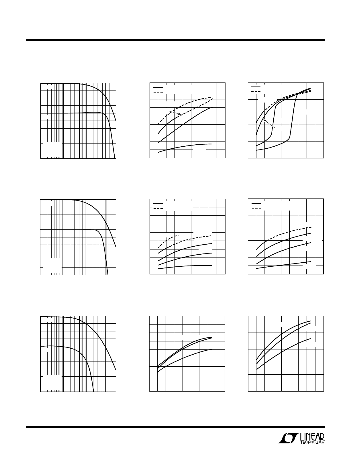
SUPPLY VOLTAGE (±V)
0
0
–3dB BANDWIDTH (MHz)
20
60
80
100
140
4
8
10 18
LT1227 • TPC06
40
160
180
120
26
12
14
16
PEAKING ≤ 0.5dB
PEAKING ≤ 5dB
RF = 500Ω
RF = 750Ω
RF = 2k
RF = 1k
SUPPLY VOLTAGE (±V)
0
0
–3dB BANDWIDTH (MHz)
2
6
8
10
14
4
8
10 18
LT1227 • TPC09
4
16
18
12
26
12
14
16
RF = 500Ω
RF = 2k
RF = 1k
LPER
F
O
R
ATYPICA
UW
CCHARA TERIST
E
C
ICS
Voltage Gain and Phase vs
Frequency, Gain = 6dB
10
PHASE
9
8
7
6
GAIN
5
4
VOLTAGE GAIN (dB)
3
2
VS = ±15V
= 100Ω
R
L
1
= 910Ω
R
F
0
0.1
1 10 100
FREQUENCY (MHz)
Voltage Gain and Phase vs
Frequency, Gain = 20dB
24
PHASE
23
22
21
20
GAIN
19
18
VOLTAGE GAIN (dB)
17
16
VS = ±15V
= 100Ω
R
L
15
= 825Ω
R
F
14
0.1
1 10 100
FREQUENCY (MHz)
LT1227 • TPC01
LT1227 • TPC04
0
PHASE SHIFT (DEG)
45
90
135
180
225
0
PHASE SHIFT (DEG)
45
90
135
180
225
–3dB Bandwidth vs Supply
Voltage, Gain = 2, RL = 100Ω
180
160
140
120
100
80
60
–3dB BANDWIDTH (MHz)
40
20
0
PEAKING ≤ 0.5dB
PEAKING ≤ 5dB
RF = 500Ω
RF = 750Ω
0
26
4
SUPPLY VOLTAGE (±V)
10 18
8
–3dB Bandwidth vs Supply
Voltage, Gain = 10, RL = 100Ω
180
160
140
120
100
80
60
–3dB BANDWIDTH (MHz)
40
20
0
PEAKING ≤ 0.5dB
PEAKING ≤ 5dB
RF = 250Ω
0
4
26
SUPPLY VOLTAGE (±V)
10 18
8
RF = 1k
RF = 2k
14
12
RF = 500Ω
RF = 750Ω
RF = 1k
RF = 2k
14
12
16
LT1227 • TPC02
16
LT1227 • TPC05
–3dB Bandwidth vs Supply
Voltage, Gain = 2, RL = 1k
180
160
140
120
100
80
60
–3dB BANDWIDTH (MHz)
40
20
0
PEAKING ≤ 0.5dB
PEAKING ≤ 5dB
RF = 750Ω
0
26
4
SUPPLY VOLTAGE (±V)
RF = 1.5k
RF = 1k
8
–3dB Bandwidth vs Supply
Voltage, Gain = 10, RL = 1k
= 2k
R
F
14
10 18
12
16
LT1227 • TPC03
44
43
42
41
40
39
38
VOLTAGE GAIN (dB)
37
36
35
34
0.1
4
Voltage Gain and Phase vs
Frequency, Gain = 40dB
PHASE
GAIN
VS = ±15V
= 100Ω
R
L
= 500Ω
R
F
1 10 100
FREQUENCY (MHz)
LT1227 • TPC07
0
PHASE SHIFT (DEG)
45
90
135
180
225
–3dB Bandwidth vs Supply
Voltage, Gain = 100, RL = 100Ω
18
16
14
12
10
8
6
–3dB BANDWIDTH (MHz)
4
2
0
0
26
RF = 500Ω
4
SUPPLY VOLTAGE (±V)
10 18
8
12
RF = 1k
RF = 2k
14
16
LT1227 • TPC08
–3dB Bandwidth vs Supply
Voltage, Gain = 100, RL = 1k
Page 5

LPER
FREQUENCY (Hz)
0.1
OUTPUT IMPEDANCE (Ω)
10k 1M 10M 100M
LT1227 • TPC18
0.001
100k
100
10
1
0.01
VS = ±15V
RF = RG = 2k
RF = RG = 1k
FREQUENCY (MHz)
1
0
OUTPUT VOLTAGE (V
P-P
)
5
10
15
20
25
10 100
LT1127 • TPC12
VS = ±15V
R
L
= 1k
R
F
= 1k
AV = +10
A
V
= –1
AV = +1
A
V
= +2
F
O
R
ATYPICA
UW
CCHARA TERIST
E
C
LT1227
ICS
Maximum Capacitive Load
vs Feedback Resistor
10000
RL = 1k
PEAKING ≤ 5dB
GAIN = 2
1000
100
CAPACITIVE LOAD (pF)
10
1
01 3
FEEDBACK RESISTOR (kΩ)
VS = ±5V
VS = ±15V
2
Input Common Mode Limit
vs Temperature
+
V
–0.5
–1.0
–1.5
–2.0
2.0
1.5
COMMON MODE RANGE (V)
1.0
0.5
–
V
–50
0
–25
TEMPERATURE (°C)
V+ = 2V TO 18V
V– = –2V TO –18V
50
25
75
LT1227 • TPC10
100
LT1227 • TPC13
125
Total Harmonic Distortion
vs Frequency
0.1
VS = ±15V
= 400Ω
R
L
= RG = 1k
R
F
0.01
VO = 7V
RMS
VO = 1V
TOTAL HARMONIC DISTORTION (%)
0.001
10
RMS
100 10k
1k 100k
FREQUENCY (Hz)
Output Saturation Voltage
vs Temperature
+
V
RL = ∞
≤ ±18V
±2V ≤ V
–0.5
–1.0
1.0
0.5
OUTPUT SATURATION VOLTAGE (V)
–
V
–50
S
–25 0
25 75
TEMPERATURE (°C)
LT1227 • TPC11
50 100 125
LT1227 • TPC14
Maximum Undistorted Output
vs Frequency
Output Short-Circuit Current
vs Junction Temperature
70
60
50
40
OUTPUT SHORT-CIRCUIT CURRENT (mA)
30
–50
0
–25 25
100
75 150 175125
50
TEMPERATURE (°C)
LT1227 • TPC15
Spot Noise Voltage and Current
vs Frequency
100
–i
n
10
SPOT NOISE (nV/√Hz OR pA/√Hz)
1
10
e
n
+i
n
100 10k
FREQUENCY (Hz)
1k 100k
LT1227 • TPC16
Power Supply Rejection
vs Frequency
80
60
40
20
POWER SUPPLY REJECTION (dB)
0
10k 1M 10M 100M
NEGATIVE
100k
FREQUENCY (Hz)
VS = ±15V
= 100Ω
R
L
= RG = 1k
R
F
POSITIVE
Output Impedance vs Frequency
LT1227 • TPC17
5
Page 6

LT1227
SUPPLY VOLTAGE (±V)
0
4
SUPPLY CURRENT (mA)
5
7
8
9
14
11
4
8
10 18
LT1227 • TPC21
6
12
13
10
26
12
14
16
–55°C
25°C
125°C
175°C
LPER
F
O
R
ATYPICA
UW
CCHARA TERIST
E
C
ICS
Settling Time to 10mV
vs Output Step
10
8
6
4
2
0
–2
OUTPUT STEP (V)
–4
–6
–8
–10
20
0
SETTLING TIME (ns)
40
NONINVERTING
INVERTING
60
Output Impedance in Shutdown
vs Frequency
100
10
1
OUTPUT IMPEDANCE (kΩ)
0.1
100k
1M 10M 100M
FREQUENCY (Hz)
VS = ±15V
= RG = 1k
R
F
80
LT1227 • TPC19
VS = ±15V
= 1
A
V
= 1.5k
R
F
LT1227 • TPC22
100
Settling Time to 1mV
vs Output Step
10
VS = ±15V
8
= RG = 1k
R
F
6
4
2
0
–2
OUTPUT STEP (V)
–4
–6
–8
–10
0
4
NONINVERTING
INVERTING
12
8
SETTLING TIME (µs)
Differential Phase vs Frequency
0
VS = ±15V
A
R
R
R
100k
V
L
F
G
= 2
= 1k
= 1k
= 1k
(VO)DC = 0.5V
1.0V
1.5V
2.0V
1M 10M 100M
FREQUENCY (Hz)
0.05
0.10
0.15
0.20
DIFFERENTIAL PHASE (DEG)
0.25
0.30
16
LT1227 • TPC20
LT1227 • TPC23
Supply Current vs Supply Voltage
20
Differential Gain vs Frequency
0
0.01
0.02
VS = ±15V
= 2
A
V
= 1k
R
L
= 1k
R
F
= 1k
R
G
(VO)DC = 0.5V
1.0V
2.0V
1M 10M 100M
FREQUENCY (Hz)
LT1227 • TPC24
0.03
0.04
DIFFERENTIAL GAIN (%)
0.05
0.06
100k
2nd and 3rd Harmonic Distortion
vs Frequency
–20
–30
–40
–50
DISTORTION (dBc)
–60
–70
6
1
VS = ±15V
= 2V
V
R
R
A
O
P-P
= 100Ω
L
= 820Ω
F
= 10dB
V
FREQUENCY (MHz)
2ND
10 100
3RD
LT1227 • TPC25
3rd Order Intercept vs Frequency
45
40
35
30
25
3RD ORDER INTERCEPT (dBm)
20
15
0
10 20 30 40
FREQUENCY (MHz)
VS = ±15V
= 100Ω
R
L
= 680Ω
R
F
= 75Ω
R
G
50 60
LT1227 • TPC26
Test Circuit for 3rd Order Intercept
+
LT1227
50Ω
P
–
680Ω
75Ω
MEASURE INTERCEPT AT P
50Ω
O
1227 TC
O
Page 7

LT1227
W
SPL
I
IIFED S
14k
8
S/D
+IN
CH
CURRENT
SOURCE
3
E
BIAS
W
A
TI
C
1 5
NULL
NULL
2
–IN
+
V
7
6
V
OUT
U
O
PPLICATI
A
The LT1227 is a very fast current feedback amplifier.
Because it is a current feedback amplifier, the bandwidth
is maintained over a wide range of voltage gains. The
amplifier is designed to drive low impedance loads such as
cables with excellent linearity at high frequencies.
Feedback Resistor Selection
The small-signal bandwidth of the LT1227 is set by the
external feedback resistors and the internal junction capacitors. As a result, the bandwidth is a function of the
supply voltage, the value of the feedback resistor, the
closed-loop gain and load resistor. The characteristic
curves of Bandwidth vs Supply Voltage show the effect of
a heavy load (100Ω) and a light load (1k). These curves
use a solid line when the response has less than 0.5dB of
peaking and a dashed line when the response has 0.5dB to
S
I FOR ATIO
WU
U
–
V
4
5dB of peaking. The curves stop where the response has
more than 5dB of peaking.
At a gain of two, on ±15V supplies with a 1k feedback
resistor, the bandwidth into a light load is over 140MHz,
but into a heavy load the bandwidth reduces to 120MHz.
The loading has this effect because there is a mild resonance in the output stage that enhances the bandwidth at
light loads but has its Q reduced by the heavy load. This
enhancement is only useful at low gain settlings; at a gain
of ten it does not boost the bandwidth. At unity gain, the
enhancement is so effective the value of the feedback
resistor has very little effect. At very high closed-loop
gains, the bandwidth is limited by the gain bandwidth
product of about 1GHz. The curves show that the bandwidth at a closed-loop gain of 100 is 12MHz, only one tenth
what it is at a gain of two.
1227 SS
7
Page 8

LT1227
U
O
PPLICATI
A
Small-Signal Rise Time, AV = +2
V
OUT
Capacitance on the Inverting Input
Current feedback amplifiers require resistive feedback
from the output to the inverting input for stable operation.
Take care to minimize the stray capacitance between the
output and the inverting input. Capacitance on the inverting input to ground will cause peaking in the frequency
response (and overshoot in the transient response), but it
does not degrade the stability of the amplifier.
Capacitive Loads
The LT1227 can drive capacitive loads directly when the
proper value of feedback resistor is used. The graph of
Maximum Capacitive Load vs Feedback Resistor should
be used to select the appropriate value. The value shown
is for 5dB peaking when driving a 1k load at a gain of 2. This
is a worst case condition, the amplifier is more stable at
higher gains and driving heavier loads. Alternatively, a
small resistor (10Ω to 20Ω) can be put in series with the
output to isolate the capacitive load from the amplifier
output. This has the advantage that the amplifier bandwidth is only reduced when the capacitive load is present
and the disadvantage that the gain is a function of the load
resistance.
S
I FOR ATIO
RF = 1k, RG= 1k, RL = 100Ω
WU
U
AI01
and inverting input bias current will change. The offset
voltage changes about 500µV per volt of supply mis-
match. The inverting bias current can change as much as
5.0µ A per volt of supply mismatch, though typically the
change is less than 0.5µA per volt.
Slew Rate
The slew rate of a current feedback amplifier is not
independent of the amplifier gain configuration the way
slew rate is in a traditional op amp. This is because both the
input stage and the output stage have slew rate limitations.
In the inverting mode, and for higher gains in the noninverting mode, the signal amplitude between the input pins
is small and the overall slew rate is that of the output stage.
For gains less than ten in the noninverting mode, the
overall slew rate is limited by the input stage.
The input stage slew rate of the LT1227 is approximately
125V/µ s and is set by internal currents and capacitances.
The output slew rate is set by the value of the feedback
resistors and the internal capacitances. At a gain of ten
with a 1k feedback resistor and ±15V supplies, the output
slew rate is typically 1100V/µ s. Larger feedback resistors
will reduce the slew rate as will lower supply voltages,
similar to the way the bandwidth is reduced.
The graph of Maximum Undistorted Output vs Frequency
relates the slew rate limitations to sinusoidal inputs for
various gain configurations.
Large-Signal Transient Response, AV = +10
V
OUT
Power Supplies
The LT1227 will operate from single or split supplies from
±2V (4V total) to ±15V (30V total). It is not necessary to
use equal value split supplies, however the offset voltage
8
RF = 910Ω, RG= 100Ω, RL = 400Ω
AI02
Page 9

LT1227
PPLICATI
A
V
OUT
U
O
S
I FOR ATIO
Large-Signal Transient Response, AV = +2
RF = 1k, RG= 1k, RL = 400Ω
Large-Signal Transient Response, AV = –2
WU
U
AI03
Shutdown
The LT1227 has a high impedance, low supply current
mode which is controlled by pin 8. In the shutdown mode,
the output looks like a 12pF capacitor and the supply
current drops to approximately the pin 8 current. The
shutdown pin is referenced to the positive supply through
an internal pullup circuit (see the simplified schematic).
Pulling a current of greater than 50µA from pin 8 will put
the device into the shutdown mode. An easy way to force
shutdown is to ground pin 8, using open drain (collector)
logic. Because the pin is referenced to the positive supply,
the logic used should have a breakdown voltage of greater
than the positive supply voltage. No other circuitry is
necessary as an internal JFET limits the pin 8 current to
about 100µA. When pin 8 is open, the LT1227 operates
normally.
Differential Input Signal Swing
V
OUT
AI04
RF = 1k, RG= 510Ω, RL = 400Ω
Settling Time
The characteristic curves show that the LT1227 amplifier
settles to within 10mV of final value in 40ns to 55ns for any
output step up to 10V. The curve of settling to 1mV of final
value shows that there is a slower thermal contribution up
to 20µ s. The thermal settling component comes from the
output and the input stage. The output contributes just
under 1mV per volt of output change and the input
contributes 300µV per volt of input change. Fortunately
the input thermal tends to cancel the output thermal. For
this reason the noninverting gain of two configuration
settles faster than the inverting gain of one.
AI04
The differential input swing is limited to about ±6V by an
ESD protection device connected between the inputs. In
normal operation, the differential voltage between the
input pins is small, so this clamp has no effect; however,
in the shutdown mode, the differential swing can be the
same as the input swing. The clamp voltage will then set
the maximum allowable input voltage. To allow for some
margin, it is recommended that the input signal be less
than ±5V when the device is shutdown.
Offset Adjust
Pins 1 and 5 are provided for offset nulling. A small current
to V+ or ground will compensate for DC offsets in the
device. The pins are referenced to the positive supply (see
the simplified schematic) and should be left open if unused. The offset adjust pins act primarily on the inverting
input bias current. A 10k pot connected to pins 1 and 5 with
the wiper connected to V+ will null out the bias current, but
will not affect the offset voltage much. Since the output
offset is
VO ≅ AV • VOS + (I
at higher gains (AV > 5), the VOS term will dominate. To null
out the VOS term, use a 10k pot between pins 1 and 5 with
a 150k resistor from the wiper to ground for 15V split
supplies, 47k for 5V split supplies.
–) • R
IN
F
9
Page 10

LT1227
FREQUENCY (MHz)
1
–90
INPUT CROSSTALK (dB)
–80
–70
–60
–50
–40
10 100
LT1227 TA05
U
O
PPLICATITYPICAL
SA
MUX Amplifier
The shutdown function can be effectively used to construct a MUX amplifier. A two-channel version is shown,
but more inputs could be added with suitable logic. By
configuring each amplifier as a unity-gain follower, there
is no loading by the feedback network when the amplifier
is off. The open drains of the 74C906 buffers are used to
interface the 5V logic to the shutdown pin. Feedthrough
from the unselected input to the output is –70dB at
10MHz. The differential voltage between MUX inputs V
and V
appears across the inputs of the shutdown
IN2
IN1
device, this voltage should be less than ±5V to avoid
turning on the clamp diodes discussed previously. If the
inputs are sinusoidal having a zero DC level, this implies
that the amplitude of each input should be less than
5V
. The output impedance of the off amplifier remains
P-P
high until the output level exceeds approximately 6V
P-P
at
10MHz, this sets the maximum usable output level. Switching time between inputs is about 4µs without an external
pullup. Adding a 10k pullup resistor from each shutdown
pin to V+ will reduce the switching time to 2µs but will
increase the positive supply current in shutdown by 1.5mA.
V
IN1
V
OUT
V
V
IN2
INPUT
SELECT
MUX Amplifier
15V
+
LT1227
S/D
V
OUT
–
= 1
IN
–15V
1.5k
5V
74C906
15V
+
LT1227
S/D
–
–15V
1.5k
5V
74HC04
5V
74C906
1227 TA04
V
INPUT
SELECT
OUT
MUX Output
V
= 1V
, V
IN1
P-P
IN2
= 0V
MUX Input Crosstalk vs Frequency
TA03
10
Page 11

LT1227
U
O
PPLICATITYPICAL
SA
15V
2N3904
Single Supply AC-Coupled Amplifier
Noninverting
5V
22µF
V
IN
10k
+
+
10k
LT1227
–
220µF
+
51Ω
510Ω
AV = 11
BW = 14Hz to 60MHz
3.58MHz Oscillator
1N4148
75pF
3.579545MHz
1k
15V
150k
100k
100pF
68pF
–
LT1227
+
–15V
4.7µF
+
51Ω
V
OUT
1227 TA08
V
1227 TA10
OUT
Single Supply AC-Coupled Amplifier
510Ω
AV =
BW = 14Hz to 60MHz
V
IN
V
IN
R
+ 51Ω
S
0.1µF
2.2µF
R
S
≈ 10
Inverting
5V
10k
+
10k
+
LT1227
–
220µF
+
51Ω
510Ω
Buffer with DC Nulling Loop
+
V
10k
10k
180Ω
3
2
+
–
5
LT1227
1.5k
180Ω
1
0.01µF
100k
10k
6
100k
4.7µF
+
V
+
–
OUT
LT1097
V
OUT
1227 TA09
CMOS Logic to Shutdown Interface
15V
7
3
+
LT1227
2
–
4
5V
–15V
10k
6
8
2N3904
1227 TA11
Information furnished by Linear Technology Corporation is believed to be accurate and reliable.
However, no responsibility is assumed for its use. Linear Technology Corporation makes no representation that the interconnection of its circuits as described herein will not infringe on existing patent rights.
Optional Offset Nulling circuit
R
+
V
7
3
+
LT1227
2
–
4
–
V
NULL
10k
1
6
5
R
R
NULL
NULL
0.01µF
1227 TA07
= 47k FOR VS = ±5V
= 150k FOR VS = ±15V
1227 TA12
11
Page 12

LT1227
PACKAGE DESCRIPTIO
0.290 – 0.320
(7.366 – 8.128)
0.008 – 0.018
(0.203 – 0.457)
0.385 ± 0.025
(9.779 ± 0.635)
CORNER LEADS OPTION
(4 PLCS)
0° – 15°
0.045 – 0.068
(1.143 – 1.727)
0.014 – 0.026
(0.360 – 0.660)
NOTE: LEAD DIMENSIONS APPLY TO SOLDER DIP OR TIN PLATE LEADS.
U
J8 Package
8-Lead Ceramic DIP
0.015 – 0.060
(0.381 – 1.524)
0.100 ± 0.010
(2.540 ± 0.254)
0.200
(5.080)
MAX
0.125
3.175
MIN
0.005
(0.127)
MIN
0.025
(0.635)
RAD TYP
0.405
(10.287)
MAX
87
12
65
3
4
0.220 – 0.310
(5.588 – 7.874)
0.045 – 0.068
(1.143 – 1.727)
FULL LEAD
OPTION
0.008 – 0.010
(0.203 – 0.254)
0.023 – 0.045
(0.584 – 1.143)
HALF LEAD
OPTION
8-Lead Plastic DIP
0.300 – 0.320
(7.620 – 8.128)
0.065
(1.651)
0.009 – 0.015
(0.229 – 0.381)
+0.025
0.325
–0.015
+0.635
8.255
()
–0.381
TYP
0.045 ± 0.015
(1.143 ± 0.381)
(2.540 ± 0.254)
0.045 – 0.065
(1.143 – 1.651)
0.100 ± 0.010
8-Lead Plastic SOIC
0.010 – 0.020
(0.254 – 0.508)
× 45°
0°– 8° TYP
0.016 – 0.050
0.406 – 1.270
*THESE DIMENSIONS DO NOT INCLUDE MOLD FLASH OR PROTRUSIONS.
MOLD FLASH OR PROTRUSIONS SHALL NOT EXCEED 0.006 INCH (0.15mm).
0.053 – 0.069
(1.346 – 1.752)
0.014 – 0.019
(0.355 – 0.483)
N8 Package
0.018 ± 0.003
(0.457 ± 0.076)
S8 Package
0.130 ± 0.005
(3.302 ± 0.127)
0.125
(3.175)
MIN
(0.508)
0.004 – 0.010
(0.101 – 0.254)
0.050
(1.270)
BSC
0.020
MIN
J8 0293
876
12
0.228 – 0.244
(5.791 – 6.197)
0.400
(10.160)
MAX
8
1
5
4
3
0.189 – 0.197*
(4.801 – 5.004)
7
2
0.250 ± 0.010
(6.350 ± 0.254)
5
6
3
4
N8 0392
0.150 – 0.157*
(3.810 – 3.988)
SO8 0294
12
Linear Technology Corporation
1630 McCarthy Blvd., Milpitas, CA 95035-7487
(408) 432-1900
●
FAX
: (408) 434-0507
●
TELEX
: 499-3977
LT/GP 0394 5K REV A
LINEAR TECHNOLOGY CORPORATION 1994
 Loading...