

Page 1
LT1224
Very High Speed
Operational Amplifier
EATU
F
■
Unity-Gain Stable
■
45MHz Gain-Bandwidth
■
400V/µs Slew Rate
■
7V/mV DC Gain: RL = 500Ω
■
Maximum Input Offset Voltage: 2mV
■
±12V Minimum Output Swing into 500Ω
■
Wide Supply Range: ±2.5V to ±15V
■
7mA Supply Current
■
90ns Settling Time to 0.1%, 10V Step
■
Drives All Capacitive Loads
PPLICATI
A
■
Wideband Amplifiers
■
Buffers
■
Active Filters
■
Video and RF Amplification
■
Cable Drivers
■
Data Acquisition Systems
RE
S
O
U
S
DUESCRIPTIO
The LT1224 is a very high speed operational amplifier with
excellent DC performance. The LT1224 features reduced
input offset voltage and higher DC gain than devices with
comparable bandwidth and slew rate. The circuit is a
single gain stage with outstanding settling characteristics.
The fast settling time makes the circuit an ideal choice for
data acquisition systems. The output is capable of driving
a 500Ω load to ±12V with ± 15V supplies and a 150Ω load
to ±3V on ±5V supplies. The circuit is also capable of
driving large capacitive loads which makes it useful in
buffer or cable driver applications.
The LT1224 is a member of a family of fast, high performance amplifiers that employ Linear Technology
Corporation’s advanced bipolar complementary
processing.
U
O
A
PPLICATITYPICAL
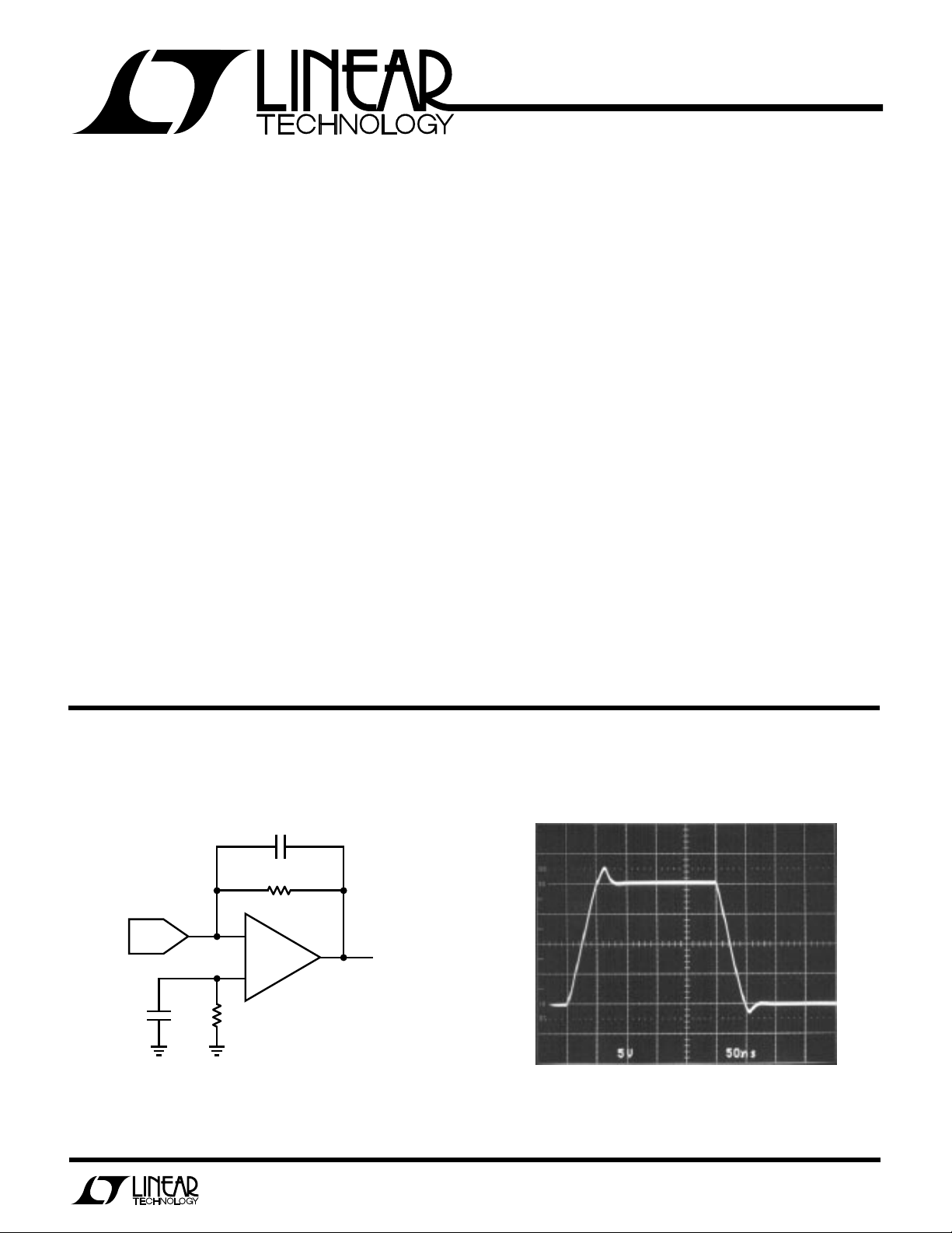
DAC Current-to-Voltage Converter Inverter Pulse Response
7pF
5k
DAC-08
TYPE
0.1µF 5k 1 LSB SETTLING = 140ns
–
+
LT1224
V
OUT
LT1224 • TA01
LT1224 • TA02
1
Page 2
LT1224
WU
U
PACKAGE
/
O
RDER I FOR ATIO
W
O
A
LUTEXI T
S
Total Supply Voltage (V+ to V–) ............................... 36V
Differential Input Voltage .........................................±6V
Input Voltage ............................................................±V
Output Short Circuit Duration (Note 1) ............Indefinite
Operating Temperature Range
LT1224C................................................ 0°C to 70°C
Maximum Junction Temperature
Plastic Package .............................................. 150°C
Storage Temperature Range ................. – 65°C to 150°C
A
WUW
ARB
U
G
I
S
S
TOP VIEW
1NULL
2
–IN
+IN
3
–
V
N8 PACKAGE
8-LEAD PLASTIC DIP
T
= 150°C, θJA = 100°C/W (N8)
JMAX
T
= 150°C, θJA = 150°C/W (S8)
JMAX
NULL
8
+
7
V
6
OUT
54
NC
S8 PACKAGE
8-LEAD PLASTIC SOIC
LT1224 • POI01
ORDER PART
NUMBER
LT1224CN8
LT1224CS8
S8 PART MARKING
1224
Lead Temperature (Soldering, 10 sec.)................. 300°C
LECTRICAL C CHARA TERIST
E
SYMBOL PARAMETER CONDITIONS MIN TYP MAX UNITS
V
OS
I
OS
I
B
e
n
i
n
R
IN
C
IN
CMRR Common-Mode Rejection Ratio VCM = ±12V 86 100 dB
PSRR Power Supply Rejection Ratio VS = ±5V to ±15V 75 84 dB
A
VOL
V
OUT
I
OUT
SR Slew Rate A
GBW Gain-Bandwidth f = 1MHz 45 MHz
tr, t
f
t
s
R
O
I
S
Input Offset Voltage (Note 2) 0.5 2.0 mV
Input Offset Current 100 400 nA
Input Bias Current 48 µA
Input Noise Voltage f = 10kHz 22 nV/√Hz
Input Noise Current f = 10kHz 1.5 pA/√Hz
Input Resistance VCM = ±12V 24 40 MΩ
Input Capacitance 2pF
Input Voltage Range
Input Voltage Range
Large-Signal Voltage Gain V
Output Swing RL = 500Ω±12.0 ±13.3 V
Output Current V
Full Power Bandwidth 10V Peak, (Note 4) 6.4 MHz
Rise Time, Fall Time A
Overshoot A
Propagation Delay 50% VIN to 50% V
Settling Time 10V Step, 0.1% 90 ns
Differential Gain f = 3.58MHz, RL = 150Ω 1%
Differential Phase f = 3.58MHz, RL = 150Ω 2.4 Deg
Output Resistance A
Supply Current 79 mA
+
–
ICS
VS = ±15V, TA = 25°C, RL = 1k, VCM = 0V unless otherwise noted.
Differential 250 kΩ
12 14 V
–13 –12 V
= ±10V, RL = 500Ω 3.3 7 V/mV
OUT
= ±12V 24 40 mA
OUT
= –2, (Note 3) 250 400 V/µs
VCL
= 1, 10% to 90%, 0.1V 5 ns
VCL
= 1, 0.1V 30 %
VCL
OUT
= 1, f = 1MHz 2.5 Ω
VCL
5ns
2
Page 3
LT1224
LECTRICAL C CHARA TERIST
E
SYMBOL PARAMETER CONDITIONS MIN TYP MAX UNITS
V
OS
I
OS
I
B
CMRR Common-Mode Rejection Ratio VCM = ±2.5V 86 98 dB
A
VOL
V
OUT
I
OUT
SR Slew Rate A
GBW Gain-Bandwidth f = 1MHz 34 MHz
tr, t
f
t
s
I
S
Input Offset Voltage (Note 2) 1 4 mV
Input Offset Current 100 400 nA
Input Bias Current 48 µA
Input Voltage Range
Input Voltage Range
Large-Signal Voltage Gain V
Output Swing RL = 500Ω±3.0 ±3.7 V
Output Current V
Full Power Bandwidth 3V Peak, (Note 4) 13.3 MHz
Rise Time, Fall Time A
Overshoot A
Propagation Delay 50% VIN to 50% V
Settling Time –2.5V to 2.5V, 0.1% 90 ns
Supply Current 79 mA
+
–
ICS
VS = ±5V, TA = 25°C, RL = 1k, VCM = 0V unless otherwise noted.
2.5 4 V
–3 – 2.5 V
= ±2.5V, RL = 500Ω 2.5 7 V/mV
OUT
= ±2.5V, RL = 150Ω 3 V/mV
V
OUT
= 150Ω±3.0 ±3.3 V
R
L
= ±3V 20 40 mA
OUT
= –2, (Note 3) 250 V/µs
VCL
= 1, 10% to 90%, 0.1V 7 ns
VCL
= 1, 0.1V 20 %
VCL
OUT
7ns
LECTRICAL C CHARA TERIST
E
SYMBOL PARAMETER CONDITIONS MIN TYP MAX UNITS
V
OS
I
OS
I
B
CMRR Common-Mode Rejection Ratio VS = ±15V, VCM = ±12V and VS = ±5V, VCM = ±2.5V 83 98 dB
PSRR Power Supply Rejection Ratio VS = ±5V to ±15V 73 84 dB
A
VOL
V
OUT
I
OUT
SR Slew Rate VS = ±15V, A
I
S
Note 1: A heat sink may be required to keep the junction temperature
below absolute maximum when the output is shorted indefinitely.
Note 2: Input offset voltage is tested with automated test equipment
in <1 second.
Input Offset Voltage VS = ±15V, (Note 2) 1 4 mV
VS = ±5V, (Note 2) 2 5 mV
Input V
Input Offset Current VS = ±15V and VS = ±5V 100 600 nA
Input Bias Current VS = ±15V and VS = ±5V 4 9 µA
Large-Signal Voltage Gain VS = ±15V, V
Output Swing VS = ±15V, RL = 500Ω±12.0 ±13.3 V
Output Current VS = ±15V, V
Supply Current VS = ±15V and VS = ±5V 7 10.5 mA
Drift 25 µV/°C
OS
= ±5V, V
V
S
VS = ±5V, RL = 500Ω or 150Ω±3.0 ±3.3 V
= ±5V, V
V
S
0°C ≤ TA ≤ 70°C, RL = 1k, VCM = 0V unless otherwise noted.
ICS
= ±10V, RL = 500Ω 2.5 7 V/mV
OUT
= ±2.5V, RL = 500Ω 2.0 7 V/mV
OUT
= ±12V 24 40 mA
OUT
= ±3V 20 40 mA
OUT
= –2, (Note 3) 250 400 V/µs
VCL
Note 3: Slew rate is measured in a gain of –2 between ±10V on the output
with ±6V on the input for ±15V supplies and ±2V on the output with
±1.75V on the input for ±5V supplies.
Note 4: Full power bandwidth is calculated from the slew rate
measurement: FPBW = SR/2πVp.
3
Page 4

LT1224
LOAD RESISTANCE (Ω)
10
50
OPEN-LOOP GAIN (dB)
80
90
100
100 1k 10k
LT1224 • TPC06
70
60
TA = 25°C
VS = ±15V
VS = ±5V
SUPPLY VOLTAGE (±V)
0
0
OUTPUT VOLTAGE SWING (V)
5
10
15
20
5101520
LT1224 • TPC03
TA = 25°C
R
L
= 500Ω
∆V
OS
= 30mV
+V
SW
–V
SW
UW
Y
PICA
20
15
LPER
F
O
R
AT
CCHARA TERIST
E
C
ICS
Input Common-Mode Range vs Output Voltage Swing vs
Supply Voltage Supply Current vs Supply Voltage Supply Voltage
8.0
TA = 25°C
< 1mV
∆V
OS
TA = 25°C
7.5
10
5
MAGNITUDE OF INPUT VOLTAGE (V)
0
0
+V
CM
–V
5101520
SUPPLY VOLTAGE (±V)
CM
LT1224 • TPC01
7.0
SUPPLY CURRENT (mA)
6.5
6.0
0
5101520
SUPPLY VOLTAGE (±V)
LT1224 • TPC02
Output Voltage Swing vs Input Bias Current vs Input Open-Loop Gain vs
Resistive Load Common-Mode Voltage Resistive Load
30
TA = 25°C
= 30mV
∆V
25
20
15
10
OUTPUT VOLTAGE SWING (Vp-p)
OS
5
0
10
100 1k 10k
LOAD RESISTANCE (Ω)
VS = ±15V
VS = ±5V
LT1224 • TPC04
5.0
VS = ±15V
= 25°C
T
A
+
+ I
I
B
IB =
4.5
2
4.0
3.5
INPUT BIAS CURRENT (µA)
3.0
–15
INPUT COMMON-MODE VOLTAGE (V)
B–
–5 5
–10 0 10 15
LT1224 • TPC05
Supply Current vs Temperature Input Bias Current vs Temperature Temperature
10
VS = ±15V
9
8
7
6
SUPPLY CURRENT (mA)
5
4
–50
4
–25 25 75 125
TEMPERATURE (°C)
100500
LT1224 • TPC07
INPUT BIAS CURRENT (µA)
50
4.75
4.5
4.25
4.0
3.75
3.5
–25 25 75 125
–50
TEMPERATURE (°C)
VS = ±15V
+
+ I
I
B
IB =
2
LT1224 • TPC08
Output Short Circuit Current vs
55
B–
100500
50
45
40
35
30
OUTPUT SHORT-CIRCUIT CURRENT (mA)
25
–50
SOURCE
–25 25 75 125
TEMPERATURE (°C)
VS = ±5V
SINK
100500
LT1224 • TPC09
Page 5

UW
TEMPERATURE (°C)
–50
200
SLEW RATE (V/µs)
300
350
450
500
–25 25 75 125
LT1224 • TPC18
100500
250
400
VS = ±15V
A
V
= –2
–SR
+SR
FREQUENCY (Hz)
1M
–10
VOLTAGE MAGNITUDE (dB)
–6
–4
0
4
6
10
10M 100M
LT1224 • TPC15
VS = ±15V
T
A
= 25°C
A
V
= –1
–8
–2
2
8
C = 1000pF
C = 0
C = 50pF
C = 100pF
C = 500pF
Y
PICA
10000
1000
100
INPUT VOLTAGE NOISE (nV/√Hz)
10
80
60
40
20
VOLTAGE GAIN (dB)
0
–20
100
LPER
F
O
R
AT
CCHARA TERIST
E
C
ICS
Power Supply Rejection Ratio vs Common Mode Rejection Ratio vs
Input Noise Spectral Density Frequency Frequency
100
VS = ±15V
= 25°C
T
A
= +101
A
V
= 100k
R
S
i
n
e
n
10 1k 10k 100k
100
FREQUENCY (Hz)
LT1224 • TPC10
10
1
0.1
100
INPUT CURRENT NOISE (pA/√Hz)
80
60
40
20
POWER SUPPLY REJECTION RATIO (dB)
0
100
1k 100k 1M 100M
+PSRR
–PSRR
FREQUENCY (Hz)
VS = ±15V
= 25°C
T
A
10M10k
LT1224 • TPC11
120
100
80
60
40
20
COMMON-MODE REJECTION RATIO (dB)
0
1k 100k 1M 100M
FREQUENCY (Hz)
Voltage Gain and Phase vs Frequency Response vs
Frequency Output Swing vs Settling Time Capacitive Load
VS = ±15V
VS = ±5V
VS = ±15V
VS = ±5V
TA = 25°C
1k 100k 1M 100M
FREQUENCY (Hz)
10M10k
LT1224 • TPC14
100
PHASE MARGIN (DEGREES)
80
60
40
20
0
10
VS = ±15V
8
= 25°C
T
A
10mV SETTLING
6
4
2
0
–2
OUTPUT SWING (V)
–4
–6
–8
–10
AV = +1 AV = –1
AV = +1 AV = –1
0 60 80 120
40
SETTLING TIME (ns)
10020
LT1224 • TPC13
LT1224
VS = ±15V
= 25°C
T
A
10M10k
LT1224 • TPC12
Closed-Loop Output Impedance vs
Frequency Gain-Bandwidth vs Temperature Slew Rate vs Temperature
100
VS = ±15V
T
A
10
1
OUTPUT IMPEDANCE (Ω)
0.1
0.01
10k
= 25°C
A
= 1
V
100k 1M 10M 100M
FREQUENCY (Hz)
LT1224 • TPC16
48
47
46
45
44
GAIN BANDWIDTH (MHz)
43
42
–25 25 75 125
–50
TEMPERATURE (°C)
VS = ±15V
100500
LT1224 • TPC17
5
Page 6

LT1224
PPLICATI
A
U
O
S
I FOR ATIO
WU
U
The LT1224 may be inserted directly into HA2541, HA2544,
AD847, EL2020 and LM6361 applications, provided that
the nulling circuitry is removed. The suggested nulling
circuit for the LT1224 is shown below.
Offset Nulling
+
V
5k
1
+
LT1224
–
8
7
4
–
V
3
2
0.1µF
6
0.1µF
LT1224 • TA03
Layout and Passive Components
As with any high speed operational amplifier, care must be
taken in board layout in order to obtain maximum performance. Key layout issues include: use of a ground plane,
minimization of stray capacitance at the input pins, short
lead lengths, RF-quality bypass capacitors located close
to the device (typically 0.01µF to 0.1µF), and use of low
ESR bypass capacitors for high drive current applications
(typically 1µF to 10µF tantalum). Sockets should be
avoided when maximum frequency performance is
required, although low profile sockets can provide
reasonable performance up to 50MHz. For more details
see Design Note 50. Feedback resistor values greater than
5k are not recommended because a pole is formed with the
input capacitance which can cause peaking. If feedback
resistors greater than 5k are used, a parallel
capacitor of 5pF to 10pF should be used to cancel the input
pole and optimize dynamic performance.
Transient Response
The LT1224 gain bandwidth is 45MHz when measured at
f = 1MHz. The actual frequency response in unity-gain is
considerably higher than 45MHz due to peaking caused by
a second pole beyond the unity-gain crossover. This is
reflected in the 50° phase margin and shows up as
overshoot in the unity-gain small-signal transient response. Higher noise gain configurations exhibit less
overshoot as seen in the inverting gain of one response.
Small Signal, AV = 1 Small Signal, AV = –1
LT1224 • TA04
The large-signal responses in both inverting and noninverting gain show symmetrical slewing characteristics.
Normally the noninverting response has a much faster
rising edge than falling edge due to the rapid change in
input common-mode voltage which affects the tail current
of the input differential pair. Slew enhancement circuitry
has been added to the LT1224 so that the noninverting
slew rate response is balanced.
Large Signal, AV = 1 Large Signal, AV = –1
LT1224 • TA06
Input Considerations
Resistors in series with the inputs are recommended for
the LT1224 in applications where the differential input
voltage exceeds ±6V continuously or on a transient basis.
An example would be in noninverting configurations with
high input slew rates or when driving heavy capacitive
loads. The use of balanced source resistance at each input
is recommended for applications where DC accuracy must
be maximized.
6
Page 7

LT1224
LT1224 • TA07
R2
1k
+
–
IN
V
OUT
V
R1
1k
R3
75
Ω
R4
75
Ω
75 CABLE
Ω
LT1224
PPLICATI
A
U
O
S
I FOR ATIO
WU
U
Capacitive Loading
The LT1224 is stable with all capacitive loads. This is
accomplished by sensing the load induced output pole and
adding compensation at the amplifier gain node. As the
capacitive load increases, both the bandwidth and phase
margin decrease so there will be peaking in the frequency
domain and in the transient response. The photo of the
small-signal response with 1000pF load shows 50% peaking. The large-signal response with a 10,000pF load shows
the output slew rate being limited by the short-circuit
current.
AV = –1, CL = 1000pF AV = 1, CL = 10,000pF
LT1224 • TA06
The LT1224 can drive coaxial cable directly, but for best
pulse fidelity the cable should be doubly terminated with
a resistor in series with the output.
Cable Driving
DAC Current-to-Voltage Converter
The wide bandwidth, high slew rate and fast settling time
of the LT1224 make it well-suited for current-to-voltage
conversion after current output D/A converters. A typical
application is shown on the first page of this data sheet
with a DAC-08 type converter with a full-scale output of
2mA. A compensation capacitor is used across the feedback resistor to null the pole at the inverting input caused
by the DAC output capacitance. The combination of the
LT1224 and DAC settles to 40mV in 140ns for both a 0V
to 10V step and for a 10V to 0V step.
U
O
CA
PPLICATITYPI
L
1MHz, 2nd Order Butterworth Filter
R2
619Ω
C2
100pF
R1
619Ω
V
IN
–38dB AT 10MHz
SMALL SIGNAL OVERSHOOT = 10%
R3
825Ω
C1
500pF
Information furnished by Linear Technology Corporation is believed to be accurate and reliable.
However, no responsibility is assumed for its use. Linear Technology Corporation makes no representation that the interconnection of circuits as described herein will not infringe on existing patent rights.
SA
Two Op Amp Instrumentation Amplifier
–
+
R4
10k
LT1224
LT1224 • TA09
V
OUT
R5
220Ω
–
+
LT1224
R1
10k
V
OUT
–
V
IN
–
+
LT1224
R2
1k
R3
1k
+
12R2
R4
AV = 1 + + + = 102
[
R3
LT1224 • TA08
TRIM R5 FOR GAIN
TRIM R1 FOR COMMON-MODE REJECTION
BW = 430kHz
R3
(
R1
R2 + R3
)
R4
]
R5
7
Page 8

LT1224
E
NULL
1 8
W
A
W
SPL
I
IIFED S
CH
V+
7
3
4V–
PACKAGEDESCRIPTI
TI
O
C
BIAS 1
–IN+IN
2
BIAS 2
U
Dimensions in inches (millimeters) unless otherwise noted.
6 OUT
LT1224 • TA10
0°– 8° TYP
0.300 – 0.320
(7.620 – 8.128)
0.009 - 0.015
(0.229 - 0.381)
+0.025
0.325
–0.015
+0.635
8.255
()
–0.381
0.010 – 0.020
(0.254 – 0.508)
0.016 – 0.050
0.406 – 1.270
× 45°
0.008 – 0.010
(0.203 – 0.254)
0.045 – 0.065
(1.143 – 1.651)
0.065
(1.651)
TYP
0.045 ± 0.015
(1.143 ± 0.381)
0.100 ± 0.010
(2.540 ± 0.254)
0.053 – 0.069
(1.346 – 1.753)
0.014 – 0.019
(0.356 – 0.483)
N8 Package
8-Lead Plastic DIP
0.130 ± 0.005
(3.302 ± 0.127)
S8 Package
8-Lead Plastic SOIC
0.050
(1.270)
BSC
0.125
(3.175)
MIN
(0.508)
0.018 ± 0.003
(0.457 ± 0.076)
0.004 – 0.010
(0.102 – 0.254)
0.020
MIN
8
1234
0.228 – 0.244
(5.791 – 6.198)
0.400
(10.160)
MAX
76
0.189 – 0.197
(4.801 – 5.004)
7
8
5
6
0.250 ± 0.010
(6.350 ± 0.254)
N8 1291
5
0.150 – 0.157
(3.810 – 3.988)
8
Linear Technology Corporation
1630 McCarthy Blvd., Milpitas, CA 95035-7487
(408) 432-1900
●
FAX
: (408) 434-0507
●
TELEX
: 499-3977
1
LINEAR TECHNOLOGY CORPORATION 1991
3
2
4
LT/GP 1192 5K REV A
S8 1291
 Loading...