

Page 1
LT1223
100MHz Current
Feedback Amplifier
EATU
F
■
100MHz Bandwidth at AV = 1
■
1000V/µs Slew Rate
■
Wide Supply Range: ±5V to ±15V
■
1mV Input Offset Voltage
■
1µA Input Bias Current
■
5MΩ Input Resistance
■
75ns Settling Time to 0.1%
■
50mA Output Current
■
6mA Quiescent Current
PPLICATI
A
■
Video Amplifiers
■
Buffers
■
IF and RF Amplification
■
Cable Drivers
■
8-, 10-, 12-Bit Data Acquisition Systems
RE
S
O
U
S
DUESCRIPTIO
The LT1223 is a 100MHz current feedback amplifier with
very good DC characteristics. The LT1223’s high slew
rate, 1000V/µs, wide supply range, ±15V, and large output
drive, ±50mA, make it ideal for driving analog signals over
double- terminated cables. The current feedback amplifier
has high gain bandwidth at high gains, unlike conventional
op amps.
The LT1223 comes in the industry standard pinout and
can upgrade the performance of many older products.
The LT1223 is manufactured on Linear Technology’s
proprietary complementary bipolar process.
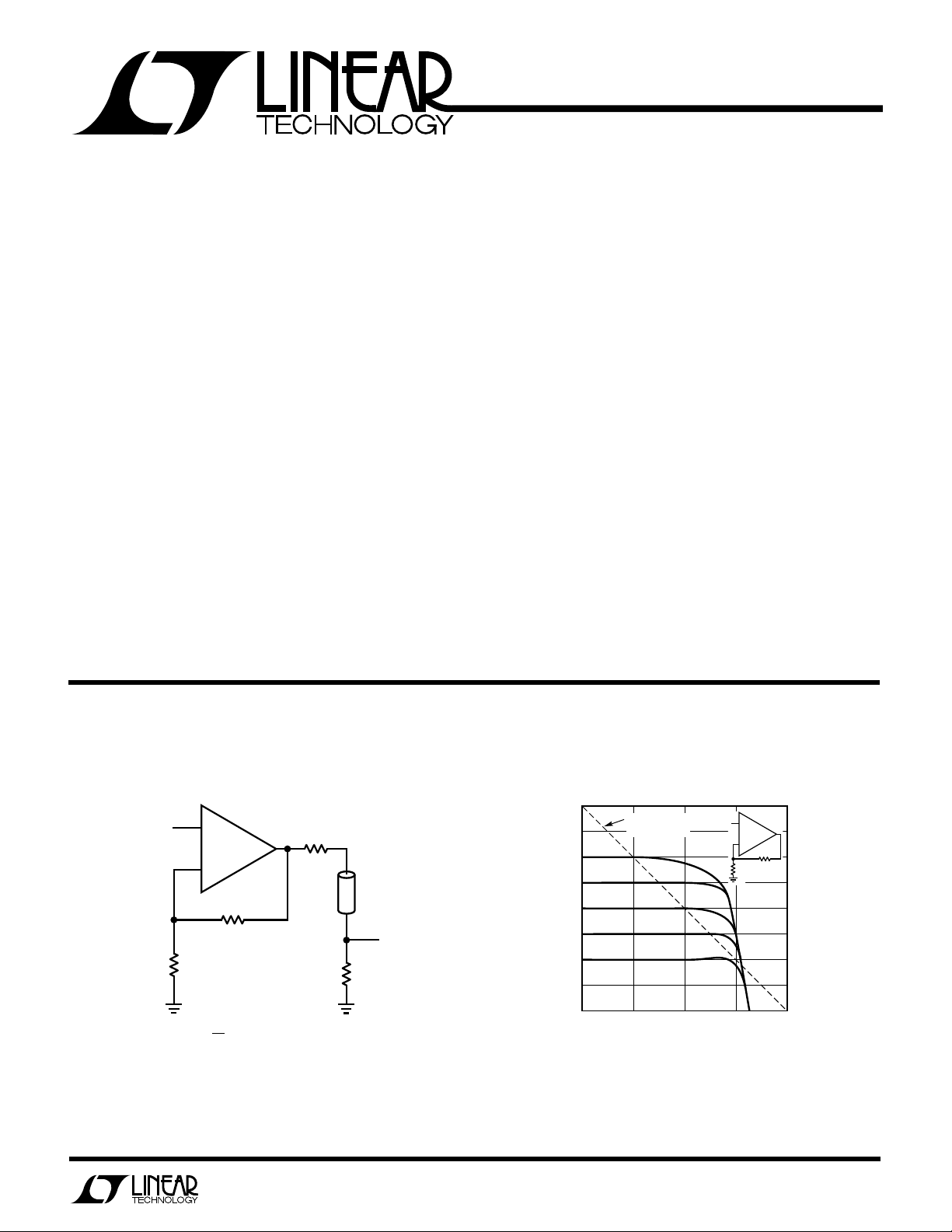
CA
A
PPLICATITYPI
L
V
+
IN
LT1223
–
RG
1k
RF
A = 1 +
V
R
AT AMPLIFIER OUTPUT.
6dB LESS AT V .
U
O
Video Cable Driver Voltage Gain vs Frequency
60
Ω
75
75
R
F
1k
G
OUT
Ω
CABLE
Ω
75
LT1223 • TA02
V
OUT
50
40
30
20
10
VOLTAGE GAIN (dB)
0
–10
–20
100k
RG = 10
R
= 33
G
= 110
R
G
R
= 470
G
R
= ∞
G
100MHz GAIN
BANDWIDTH
1M
10M 100M 1G
FREQUENCY (Hz)
+
–
1k
R
G
LT1223 • TPC01
1
Page 2
LT1223
WU
U
PACKAGE
/
O
RDER I FOR ATIO
W
O
A
LUTEXI T
S
Supply Voltage ...................................................... ±18V
Differential Input Voltage ......................................... ±5V
Input Voltage ............................ Equal to Supply Voltage
Output Short Circuit Duration (Note 1) .........Continuous
Operating Temperature Range
LT1223M........................................ –55°C to 125°C
LT1223C................................................ 0°C to 70°C
Storage Temperature Range ................. –65°C to 150°C
Junction Temperature Plastic Package...........150°C
Junction Temperature Ceramic Package ........ 175°C
Lead Temperature (Soldering, 10 sec.)................. 300°C
LECTRICAL C CHARA TERIST
E
SYMBOL PARAMETER CONDITIONS MIN TYP MAX UNITS
V
OS
I
+ Noninverting Input Current VCM = 0V ±1 ±3 µA
IN
IIN– Inverting Input Current VCM = 0V ±1 ±3 µA
e
n
i
n
R
IN
C
IN
CMRR Common-Mode Rejection Ratio VCM = ±10V 56 63 dB
PSRR Power Supply Rejection Ratio VS = ±4.5V to ±18V 68 80 dB
A
V
R
OL
V
OUT
I
OUT
SR Slew Rate RF = 1.5k, RG = 1.5k, (Note 2) 800 1300 V/µs
BW Bandwidth RF = 1k, RG = 1k, V
t
r
t
PD
t
s
R
OUT
I
S
Input Offset Voltage VCM = 0V ±1 ±3mV
Input Noise Voltage Density f = 1kHz, RF = 1k, RG = 10Ω 3.3 nV/√Hz
Input Noise Current Density f = 1kHz, RF = 1k, RG = 10Ω 2.2 pA/√Hz
Input Resistance VIN = ±10V 1 10 MΩ
Input Capacitance 1.5 pF
Input Voltage Range ±10 ±12 V
Inverting Input Current Common-Mode Rejection VCM = ±10V 30 100 nA/ V
Noninverting Input Current Power Supply Rejection VS = ±4.5V to ±18V 12 100 nA/V
Inverting Input Current Power Supply Rejection VS = ±4.5V to ±18V 60 500 nA/V
Large Signal Voltage Gain R
Transresistance, ∆V
Maximum Output Voltage Swing R
Maximum Output Current R
Rise Time RF = 1.5k, RG = 1.5k, V
Propagation Delay RF = 1.5k, RG = 1.5k, V
Overshoot RF = 1.5k, RG = 1.5k, V
Settling Time, 0.1% RF = 1k, RG = 1k, V
Differential Gain RF = 1k, RG = 1k, RL = 150Ω 0.02 %
Differential Phase RF = 1k, RG = 1k, RL = 150Ω 0.12 Deg
Open-Loop Output Resistance V
Supply Current VIN = 0V 6 10 mA
Supply Current, Shutdown Pin 8 Current = 200µA24mA
A
WUW
ARB
/∆IIN–R
OUT
U
G
S
I
1NULL
2
–IN
+IN
3
–
V
J8 PACKAGE
8-LEAD CERAMIC DIP
8-LEAD PLASTIC SOIC
T
= 175°C, θJA = 100°C/W(J8)
J MAX
T
= 150°C, θJA = 100°C/W(N8)
J MAX
T
= 150°C, θJA = 150°C/W(S8)
J MAX
VS = ±15V, TA = 25°C, unless otherwise noted.
ICS
= 400Ω, V
LOAD
= 400Ω, V
LOAD
= 200Ω±10 ±12 V
LOAD
= 200Ω 50 60 mA
LOAD
= 0, I
OUT
OUT
= ±10V 70 89 dB
OUT
= ±10V 1.5 5 MΩ
OUT
= 100mV 100 MHz
OUT
OUT
OUT
OUT
= 10V 75 ns
OUT
= 0 35 Ω
TOP VIEW
SHUTDOWN
8
+
7
V
6
OUT
54
NULL
N8 PACKAGE
8-LEAD PLASTIC DIP
S8 PACKAGE
LT1223 • POI01
LT1223M/C
= 1V 6.0 ns
= 1V 6.0 ns
= 1V 5 %
ORDER PART
NUMBER
LT1223MJ8
LT1223CJ8
LT1223CN8
LT1223CS8
S8 PART MARKING
1223
2
Page 3
LT1223
LECTRICAL C CHARA TERIST
E
SYMBOL PARAMETER CONDITIONS MIN TYP MAX UNITS
V
OS
I
+ Noninverting Input Current VCM = 0V ● ±1 ±3 µA
IN
IIN– Inverting Input Current VCM = 0V ● ±1 ±3 µA
R
IN
CMRR Common-Mode Rejection Ratio VCM = ±10V ● 56 63 dB
PSRR Power Supply Rejection Ratio VS = ±4.5V to ±18V ● 68 80 dB
A
V
R
OL
V
OUT
I
OUT
I
S
Input Offset Voltage VCM = 0V ● ±1 ±3mV
Input Resistance VIN = ±10V ● 110 MΩ
Input Voltage Range ● ±10 ±12 V
Inverting Input Current Common-Mode Rejection VCM = ±10V ● 30 100 nA/V
Noninverting Input Current Power Supply Rejection VS = ±4.5V to ±18V ● 12 100 nA/V
Inverting Input Current Power Supply Rejection VS = ±4.5V to ±18V ● 60 500 nA/ V
Large-Signal Voltage Gain R
Transresistance, ∆V
Maximum Output Voltage Swing R
Maximum Output Current R
Supply Current VIN = 0V ● 610 mA
Supply Current, Shutdown Pin 8 Current = 200µA ● 24 mA
/∆IIN–R
OUT
VS = ±15V, VCM = 0V, 0°C ≤ TA ≤ 70°C, unless otherwise noted.
ICS
= 400Ω, V
LOAD
= 400Ω, V
LOAD
= 200Ω ● ±10 ±12 V
LOAD
= 200Ω ● 50 60 mA
LOAD
= ±10V ● 70 89 dB
OUT
= ±10V ● 1.5 5 MΩ
OUT
LT1223C
LECTRICAL C CHARA TERIST
E
SYMBOL PARAMETER CONDITIONS MIN TYP MAX UNITS
V
OS
I
+ Noninverting Input Current VCM = 0V ● ±1 ±5 µA
IN
IIN– Inverting Input Current VCM = 0V ● ±1 ±10 µA
R
IN
CMRR Common-Mode Rejection Ratio VCM = ±10V ● 56 63 dB
PSRR Power Supply Rejection Ratio VS = ±4.5V to ±15V ● 68 80 dB
A
V
R
OL
V
OUT
I
OUT
I
S
● denotes the specifications which apply over the full operating
The
temperature range.
Note 1: A heat sink may be required.
Note 2: Noninverting operation, V
Input Offset Voltage VCM = 0V ● ±1 ±5mV
Input Resistance VIN = ±10V ● 110 MΩ
Input Voltage Range ● ±10 ±12 V
Inverting Input Current Common-Mode Rejection VCM = ±10V ● 30 100 nA/V
Noninverting Input Current Power Supply Rejection VS = ±4.5V to ±15V ● 12 200 nA/V
Inverting Input Current Power Supply Rejection VS = ±4.5V to ±15V ● 60 500 nA/V
Large-Signal Voltage Gain R
Transresistance, ∆V
Maximum Output Voltage Swing R
Maximum Output Current R
Supply Current VIN = 0V ● 610 mA
Supply Current, Shutdown Pin 8 Current = 200µA ● 24 mA
/∆IIN–R
OUT
= ±10V, measured at ±5V.
OUT
VS = ±15V, VCM = 0V, –55°C ≤ TA ≤ 125°C, unless otherwise noted.
ICS
LT1223M
= 400Ω, V
LOAD
= 400Ω, V
LOAD
= 200Ω ● ±7 ±12 V
LOAD
= 200Ω ● 35 60 mA
LOAD
= ±10V ● 70 89 dB
OUT
= ±10V ● 1.5 5 MΩ
OUT
3
Page 4
LT1223
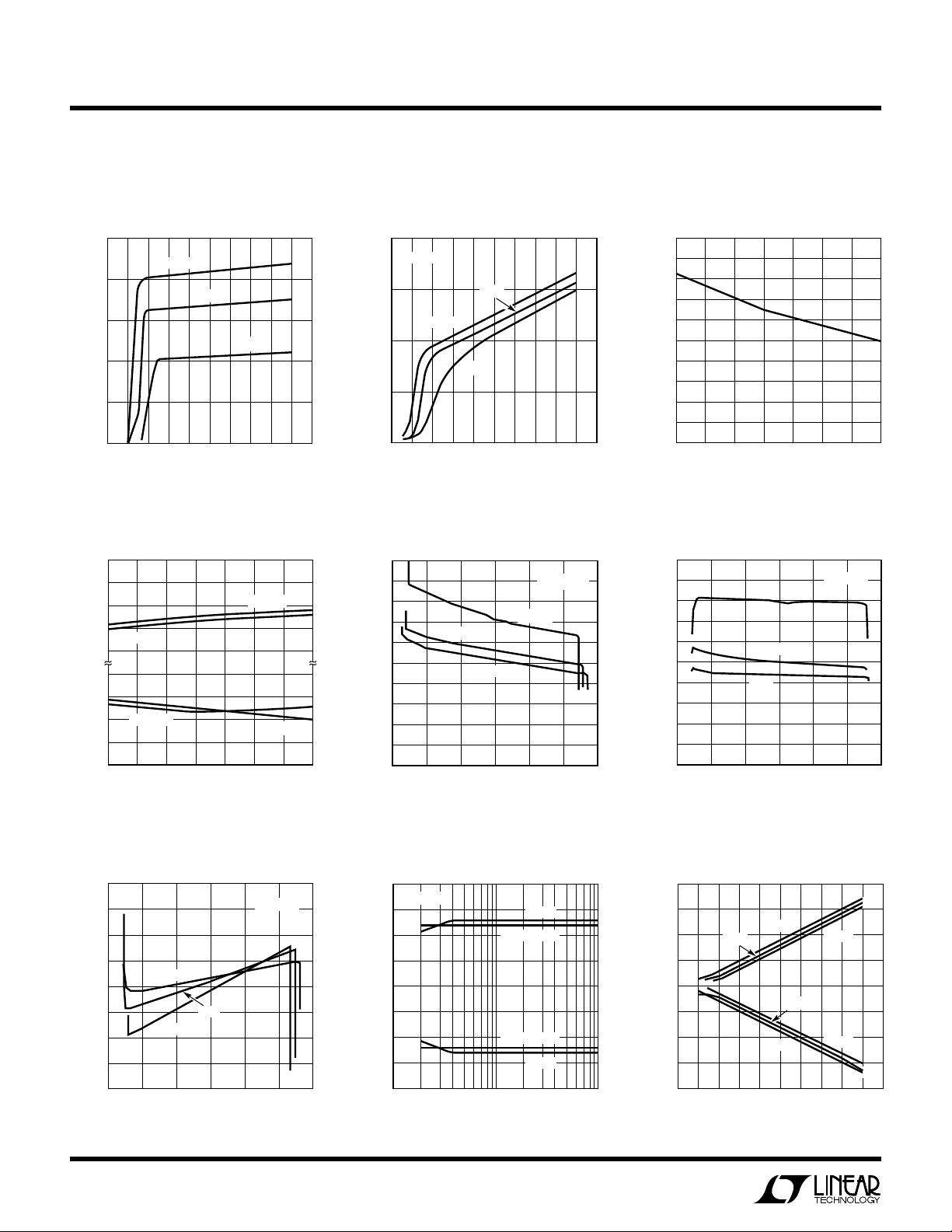
COMMON MODE VOLTAGE (V)
–15
–10
–l ( A)
–6
–2
2
6
10
LT1223 • TPC07
–10 –5 0 5 10 15
125°C
µ
–8
–4
0
4
8
–55°C
±V = 15V
S
25°C
B
CASE TEMPERATURE (°C)
–50
0
OUTPUT SHORT CIRCUIT CURRENT (mA)
30
100
LT1223 • TPC04
–25 0 25 50 75 100 125
10
20
40
50
60
70
80
90
SUPPLY VOLTAGE ( V)
0
–20
OUTPUT VOLTAGE SWING (V)
–10
–5
10
20
LT1223 • TPC10
2 4 6 8 101214161820
±
125°C
–15
0
5
15
25°C
25°C
125°C
–55°C
–55°C
UW
Y
PICA
10
8
6
4
SUPPLY CURRENT (mA)
2
LPER
F
O
R
AT
CCHARA TERIST
E
C
ICS
Supply Current vs Supply Voltage, Supply Current vs Supply Voltage Output Short Circuit-Current vs
VIN = 0 (Operating) (Shutdown) Temperature
4
125°C
25°C
–55°C
PIN 8 = 0V
3
125°C
2
SUPPLY CURRENT (mA)
1
25°C
–55°C
0
2 4 6 8 101214161820
0
SUPPLY VOLTAGE ( V)
Input Common-Mode Limit vs
Temperature +IB vs Common-Mode Voltage –IB vs Common-Mode Voltage
V+
–1
–2
–3
V = 5V
S
–4
+4
+3
V = –15V
+2
COMMON MODE RANGE (V)
S
+1
V–
–50 –25 0 25 50 75 100 125
TEMPERATURE (°C)
VOS vs Common-Mode Voltage Load Resistor Supply Voltage
20
15
10
5
0
OS
V (mV)
–5
–10
–15
–20
–15
4
125°C
–55°C
–10 –5 0 5 10 15
COMMON MODE VOLTAGE (V)
25°C
±
LT1223 • TPC02
V = 15V
S
V = –5V
S
LT1223 • TPC05
V = 15V
S
LT1223 • TPC08
0
2 4 6 8 101214161820
0
±
–55°C
LT1223 • TPC03
V = ±15V
S
LT1223 • TPC06
5
4
3
2
1
µ
0
B
+l ( A)
–1
–2
–3
–4
–5
–15
SUPPLY VOLTAGE ( V)
25°C
125°C
–10 –5 0 5 10 15
COMMON MODE VOLTAGE (V)
Output Voltage Swing vs Output Voltage Swing vs
20
±
V = 15VS±
15
10
5
0
–5
–10
OUTPUT VOLTAGE SWING (V)
–15
–20
100
LOAD RESISTOR ( )
125°C
25°C, –55°C
25°C, –55°C
125°C
1000 10000
Ω
LT1223 • TPC09
Page 5

LT1223
VOLTAGE GAIN (V/V)
0
100
FEEDBACK RESISTOR ( )
400
1000
LT1223 • TPC13
20 40 60
200
300
500
600
700
800
900
10 30 50
Ω
2dB PEAKING
0dB PEAKING
V = 15V
R = 100
S
±
L
LOAD RESISTOR ( )
100
0
TRANSIMPEDANCE (M )
10
1000 10000
LT1223 • TPC16
Ω
1
2
3
5
Ω
4
6
7
8
9
V = 15V
V = 10V
S
±
O
±
–55°C
25°C
125°C
FREQUENCY (Hz)
0.1
MAGNITUDE OF OUTPUT IMPEDANCE ( )
1
10
100
10k 1M 10M 100M
LT1223 • TPC19
0.01
100k
Ω
RF = RG = 3k
V = 15VS±
RF = RG = 1k
UW
Y
PICA
100
90
80
70
60
50
40
30
–3dB BANDWIDTH (MHz)
20
10
0
10k
1k
LPER
F
O
R
AT
CCHARA TERIST
E
C
ICS
–3dB Bandwidth vs –3dB Bandwidth vs Minimum Feedback Resistor vs
Feedback Resistor Supply Voltage Voltage Gain
100
RF = RG
90
A = 2
V
Ω
R = 100
L
80
T = 25°C
A
70
60
50
40
30
–3dB BANDWIDTH (MHz)
20
10
0
RF = 750
0
51015
SUPPLY VOLTAGE ( V)
RF = 1.5k
RF = 1k
RF = 2k
±
LT1223 • TPC12
0
123
FEEDBACK RESISTOR (k )
= RG
A = 2; R
F
V
Ω
R = 100 ; V = 15V
L
NO CAPACITIVE LOAD
±
S
Ω
LT1223 • TPC11
Maximum Capacitive Load vs Open-Loop Voltage Gain vs
Feedback Resistor Load Resistor Transimpedance vs Load Resistor
A = 2; R
= RG
F
V
R = 100; V = 15V
L
PEAKING < 5dB
±
S
100
90
80
25°C
–55°C
100
CAPACITIVE LOAD (pF)
10
0
123
FEEDBACK RESISTOR (k )
Spot Noise Voltage and Current vs Power Supply Rejection vs
Frequency Frequency Output Impedance vs Frequency
1000
–i
100
Hz Hz√√
10
SPOT NOISE (nV/ OR pA/ )
1
n
e
n
10
100 1k 10k
FREQUENCY (Hz)
70
60
OPEN LOOP VOLTAGE GAIN (dB)
50
40
100
Ω
LT1223 • TPC14
80
60
+i
n
LT1223 • TPC17
40
20
POWER SUPPLY REJECTION (dB)
0
10k 1M 10M 100M
125°C
NEGATIVE
100k
V = 15V
S
V = 10V
O
1000 10000
LOAD RESISTOR ( )
POSITIVE
FREQUENCY (Hz)
Ω
±
±
LT1223 • TPC15
V = ±15V
S
= 1k
R
F
LT1223 • TPC18
5
Page 6

LT1223
FREQUENCY (MHz)
1
–70
DISTORTION (dBc)
–20
10 100
LT1223 • TPC22
–60
–50
–40
–30
2ND
3RD
V = 15V
V = 2V
P-P
R = 100
R
F
= 1k
A = 10dB
S
±
O
L
V
UW
Y
PICA
20
15
10
5
0
–5
–10
VOLTAGE GAIN (dB)
–15
–20
–25
–30
10
8
6
4
2
0
–2
OUTPUT STEP (V)
–4
–6
–8
–10
LPER
F
O
R
AT
CCHARA TERIST
E
C
ICS
Voltage Gain and Phase vs Total Harmonic Distortion vs 2nd and 3rd Harmonic
Frequency Frequency Distortion vs Frequency
1M
GAIN
R = 100
Ω
L
PHASE
R 1k
≥
R = 100LΩ
L
10M 100M 1G
FREQUENCY (Hz)
±
V = 15V
S
= RG = 1k
R
F
R 1k
≥
L
LT1223 • TPC20
225
180
135
90
45
0
–45
–90
–135
–180
–225
0.1
V = 15V
±
S
V = 7V
RMS
O
R = 400
PHASE SHIFT (DEGREES)
0.01
TOTAL HARMONIC DISTORTION (%)
0.001
10 1k 10k 100k
L
= RG =1k
R
F
Ω
100
THD
FREQUENCY (Hz)
LT1223 • TPC21
Noninverting Amplifier Settling Noninverting Amplifier Settling Inverting Amplifier Settling
Time to 10mV vs Output Step Time to 1mV vs Output Step Time vs Output Step
A = +1
V
= 1k
R
F
V = 15V
±
S
R = 1k
L
20 40 60 80 100
0
SETTLING TIME (ns)
TO 10mV
TO 10mV
LT1223 • TPC23
10
A = +1
V
8
R = 1k
F
±
V = 15V
S
6
R = 1k
L
4
2
0
–2
OUTPUT STEP (V)
–4
–6
–8
–10
0
TO 1mV
TO 1mV
12
SETTLING TIME ( s)
µ
LT1223 • TPC24
10
A = –1
V
8
R = 1k
F
±
V = 15V
6
S
R = 1k
L
4
2
0
–2
OUTPUT STEP (V)
–4
TO 10mV
–6
–8
–10
20 40 60 80
0
TO 10mV
SETTLING TIME (ns)
TO 1mV
TO 1mV
100
LT1223 • TPC25
A
Current Feedback Basics
The small-signal bandwidth of the LT1223, like all current
feedback amplifiers, isn’t a straight inverse function of the
closed-loop gain. This is because the feedback resistors
determine the amount of current driving the amplifier’s
internal compensation capacitor. In fact, the amplifier’s
feedback resistor (RF) from output to inverting input
works with internal junction capacitances of the LT1223 to
set the closed-loop bandwidth.
Even though the gain set resistor (RG) from inverting input
to ground works with RF to set the voltage gain just like it
6
PPLICATI
O
U
S
I FOR ATIO
WU
U
does in a voltage feedback op amp, the closed-loop
bandwidth does not change. This is because the equivalent gain bandwidth product of the current feedback amplifier is set by the Thevenin equivalent resistance at the
inverting input and the internal compensation capacitor.
By keeping RF constant and changing the gain with RG, the
Thevenin resistance changes by the same amount as the
change in gain. As a result, the net closed-loop bandwidth
of the LT1223 remains the same for various closed-loop
gains.
Page 7

LT1223
U
O
PPLICATI
A
The curve on the first page shows the LT1223 voltage gain
versus frequency while driving 100Ω, for five gain settings
from 1 to 100. The feedback resistor is a constant 1k and
the gain resistor is varied from infinity to 10Ω. Shown for
comparison is a plot of the fixed 100MHz gain bandwidth
limitation that a voltage feedback amplifier would have. It
is obvious that for gains greater than one, the LT1223
provides 3 to 20 times more bandwidth. It is also evident
that second order effects reduce the bandwidth somewhat
at the higher gain settings.
Feedback Resistor Selection
Because the feedback resistor determines the compensation of the LT1223, bandwidth and transient response can
be optimized for almost every application. To increase the
bandwidth when using higher gains, the feedback resistor
(and gain resistor) can be reduced from the nominal 1k
value. The Minimum Feedback Resistor versus Voltage
Gain curve shows the values to use for ± 15V supplies.
Larger feedback resistors can also be used to slow down
the LT1223 as shown in the –3dB Bandwidth versus
Feedback Resistor curve.
Capacitive Loads
The LT1223 can be isolated from capacitive loads with a
small resistor (10Ω to 20Ω) or it can drive the capacitive
load directly if the feedback resistor is increased. Both
techniques lower the amplifier’s bandwidth about the
same amount. The advantage of resistive isolation is that
the bandwidth is only reduced when the capacitive load is
present. The disadvantage of resistor isolation is that
resistive loading causes gain errors. Because the DC
accuracy is not degraded with resistive loading, the desired way of driving capacitive loads, such as flash converters, is to increase the feedback resistor. The Maximum
Capacitive Load versus Feedback Resistor curve shows
the value of feedback resistor and capacitive load that
gives 5dB of peaking. For less peaking, use a larger
feedback resistor.
Power Supplies
The LT1223 may be operated with single or split supplies
as low as ±4V (8V total) to as high as ±18V (36V total). It
S
I FOR ATIO
WU
U
is not necessary to use equal value split supplies, however, the offset voltage will degrade about 350µV per volt
of mismatch. The internal compensation capacitor decreases with increasing supply voltage. The –3dB Bandwidth versus Supply Voltage curve shows how this affects
the bandwidth for various feedback resistors. Generally,
the bandwidth at ±5V supplies is about half the value it is
at ±15V supplies for a given feedback resistor.
The LT1223 is very stable even with minimal supply
bypassing, however, the transient response will suffer if
the supply rings. It is recommended for good slew rate and
settling time that 4.7µF tantalum capacitors be placed
within 0.5 inches of the supply pins.
Input Range
The noninverting input of the LT1223 looks like a 10M
resistor in parallel with a 3pF capacitor until the common
mode range is exceeded. The input impedance drops
somewhat and the input current rises to about 10µA when
the input comes too close to the supplies. Eventually,
when the input exceeds the supply by one diode drop, the
base collector junction of the input transistor forward
biases and the input current rises dramatically. The input
current should be limited to 10mA when exceeding the
supplies. The amplifier will recover quickly when the input
is returned to its normal common mode range unless the
input was over 500mV beyond the supplies, then it will
take an extra 100ns.
Offset Adjust
Output offset voltage is equal to the input offset voltage
times the gain plus the inverting input bias current times
the feedback resistor. For low gain applications (3 or less)
a 10kΩ pot connected to pins 1 and 5 with wiper to V+ will
trim the inverting input current (±10µA) to null the output;
it does not change the offset voltage very much. If the
LT1223 is used in a high gain application, where input
offset voltage is the dominate error, it can be nulled by
pulling approximately 100µA from pin 1 or 5. The easy way
to do this is to use a 10kΩ pot between pin 1 and 5 with a
150k resistor from the wiper to ground for 15V supply
applications. Use a 47k resistor when operating on a 5V
supply.
7
Page 8

LT1223
U
O
PPLICATI
A
Shutdown
Pin 8 activates a shutdown control function. Pulling more
than 200µA from pin 8 drops the supply current to less than
3mA, and puts the output into a high impedance state. The
easy way to force shutdown is to ground pin 8, using an
open collector (drain) logic stage. An internal resistor limits
current, allowing direct interfacing with no additional parts.
When pin 8 is open, the LT1223 operates normally.
Slew Rate
The slew rate of a current feedback amplifier is not independent of the amplifier gain configuration the way it is in
a traditional op amp. This is because the input stage and
the output stage both have slew rate limitations. Inverting
amplifiers do not slew the input and are therefore limited
only by the output stage. High gain, noninverting amplifiers are similar. The input stage slew rate of the LT1223 is
about 350V/µs before it becomes nonlinear and is en-
hanced by the normally reverse-biased emitters on the
input transistors. The output slew rate depends on the size
of the feedback resistors. The peak output slew rate is
about 2000V/µs with a 1k feedback resistor and drops
proportionally for larger values. At an output slew rate of
1000V/µs or more, the transistors in the “mirror circuits”
will begin to saturate due to the large feedback currents.
This causes the output to have slew induced overshoot and
is somewhat unusual looking; it is in no way harmful or
dangerous to the device. The photos show the LT1223 in
a noninverting gain of three (RF = 1k, RG = 500Ω) with a
20V peak-to-peak output slewing at 500V/µs, 1000V/µs
and 2000V/µs.
S
I FOR ATIO
WU
U
Output Slew Rate of 500V/µs
Output Slew Rate of 1000V/µs
Output Slew Rate at 2000V/µs Shows Aberrations (See Text)
Settling Time
The Inverting Amplifier Settling Time versus Output Step
curve shows that the LT1223 will settle to within 1mV of
final value in less than 100ns for all output changes of 10V
or less. When operated as an inverting amplifier there is
less than 500µV of thermal settling in the amplifier.
However, when operating the LT1223 as a noninverting
amplifier, there is an additional thermal settling component that is about 200µV for every volt of input common
mode change. So a noninverting gain of one amplifier will
8
Page 9

LT1223
PPLICATI
A
U
O
S
I FOR ATIO
WU
U
have about 2.5mV thermal tail on a 10V step. Unfortunately, reducing the input signal and increasing the gain
always results in a thermal tail of about the same amount
for a given output step. For this reason we show separate
graphs of 10mV and 1mV non-inverting amplifier settling
times. Just as the bandwidth of the LT1223 is fairly
constant for various closed-loop gains, the settling time
remains constant as well.
Adjustable Gain Amplifier
To make a variable gain amplifier with the LT1223, vary the
value of RG. The implementation of RG can be a pot, a light
controlled resistor, a FET, or any other low capacitance
variable resistor. The value of RF should not be varied to
change the gain. If RF is changed, then the bandwidth will
be reduced at maximum gain and the circuit will oscillate
when RF is very small.
Accurate Bandwidth Limiting The LT1223
It is very common to limit the bandwidth of an op amp by
putting a small capacitor in parallel with RF. DO NOT PUT
A SMALL CAPACITOR FROM THE INVERTING INPUT OF
A CURRENT FEEDBACK AMPLIFIER TO ANYWHERE ELSE,
ESPECIALLY NOT TO THE OUTPUT. The capacitor on the
inverting input will cause peaking or oscillations. If you
need to limit the bandwidth of a current feedback amplifier,
use a resistor and capacitor at the noninverting input (R1
& C1). This technique will also cancel (to a degree) the
peaking caused by stray capacitance at the inverting input.
Unfortunately, this will not limit the output noise the way
it does for the op amp.
V
R1
IN
+
LT1223
–
V
OUT
V
+
IN
LT1223
–
R
F
R
G
V
OUT
LT1223 • TA03
Adjustable Bandwidth Amplifier
Because the resistance at the inverting input determines
the bandwidth of the LT1223, an adjustable bandwidth
circuit can be made easily. The gain is set as before with
RF and RG; the bandwidth is maximum when the variable
resistor is at a minimum.
V
R
G
+
IN
LT1223
–
5k
R
F
V
OUT
LT1223 • TA04
R
F
R
R1 = 300C1Ω
C1 = 100pF
BW = 5MHz
G
LT1223 • TA05
Current Feedback Amplifier Integrator
Since we remember that the inverting input wants to see
a resistor, we can add one to the standard integrator
circuit. This generates a new summing node where we can
apply capacitive feedback. The LT1223 integrator has
excellent large signal capability and accurate phase shift at
high frequencies.
+
V
OUT
1
=
sC R
V
IN
V
IN
II
R
I
LT1223
–
RF
1k
C
I
V
OUT
LT1223 • TA06
9
Page 10

LT1223
RG1
1k
LT1223 • TA09
OUT
V
A1
LT1223
IN
V
A2
LT1223
IN
V
–+
++
––
R
F1
1k
RG2
1k
RF2
1k
V
OUT
= G (V
IN
+
– V
IN
–
)
R
F1
= RF2; RG1 = (G – 1) RF2; RG2 =
TRIM GAIN (G) WITH R
G2
; TRIM CMRR WITH RG1
R
F2
G – 1
PPLICATI
A
U
O
S
I FOR ATIO
WU
U
Summing Amplifier (DC Accurate)
The summing amplifier is easily made by adding additional
inputs to the basic inverting amplifier configuration. The
LT1223 has no IOS spec because there is no correlation
between the two input bias currents. Therefore, we will not
improve the DC accuracy of the inverting amplifier by
putting in the extra resistor in the noninverting input.
+
+
V
OUT
+
LT1223 • TA07
R
1
G
V
I1
R
2
G
V
I2
•
•
•
R
n
G
V
In
LT1223
–
V = –R
OUT F
R
F
V V V
I1 I2 In
( )
R R R
G1 G2 Gn
inverting input (A1) senses the shield and the non-inverting input (A2) senses the center conductor. Since this
amplifier does not load the cable (take care to minimize
stray capacitance) and it rejects common mode hum and
noise, several amplifiers can sense the signal with only
one termination at the end of the cable. The design
equations are simple. Just select the gain you need (it
should be two or more) and the value of the feedback
resistor (typically 1k) and calculate RG1 and RG2. The gain
can be tweaked with RG2 and the CMRR with RG1 if needed.
The bandwidth of the noninverting input signal is not
reduced by the presence of the other amplifier, however,
the inverting input signal bandwidth is reduced since it
passes two amplifiers. The CMRR is good at high frequencies because the bandwidth of the amplifiers are about the
same even though they do not necessarily operate at the
same gain.
Difference Amplifier
The LT1223 difference amplifier delivers excellent
performance if the source impedance is very low. This is
because the common mode input resistance is only equal
to RF + RG.
R
G
V
1
R
G
V
2
R
F
V
=
(V – V )
OUT
Video Instrumentation Amplifier
1
R
G
(RF –50)
100
+
LT1223
–
2
R
F
OPTIONAL TRIM
FOR CMRR
V
OUT
LT1223 • TA08
This instrumentation amplifier uses two LT1223s to increase the input resistance to well over 1M. This makes an
excellent “loop through” or cable sensing amplifier if the
Cable Driver
The cable driver circuit is shown on the front page. When
driving a cable it is important to properly terminate both
ends if even modest high frequency performance is
required. The additional advantage of this is that it isolates
the capacitive load of the cable from the amplifier so it can
operate at maximum bandwidth.
10
Page 11

A
LT1223
U
O
PPLICATITYPICAL
150mA Output Current Video Amp
Ω
+
V
+
V
V
IN
+
LT1223
–
IN
LT1010
20
BIAS
Ω
OUT
75
75Ω
75Ω
75Ω
W
SPL
I
IIFED S
V
2k
R = 2k TO STABILIZE CIRCUIT
f
DIFFERENTIAL GAIN = 1%
DIFFERENTIAL PHASE = 1°
W
A
E
CH
TI
15k
10k
–
2k
–
V
75Ω
75Ω
75Ω
75Ω
75Ω75Ω
LT1223 • TA10
C
7
5
BIAS
1
8
3
BIAS
Information furnished by Linear Technology Corporation is believed to be accurate and reliable.
However, no responsibility is assumed for its use. Linear Technology Corporation makes no representation that the interconnection of its circuits as described herein will not infringe on existing patent rights.
2
LT1223 • TA01
6
4
11
Page 12

LT1223
PACKAGEDESCRIPTI
0.290 – 0.320
(7.366 – 8.128)
0.008 – 0.018
(0.203 – 0.460)
0.385 ± 0.025
(9.779 ± 0.635)
0° – 15°
0.038 – 0.068
(0.965 – 1.727)
0.014 – 0.026
(0.360 – 0.660)
O
U
Dimensions in inches (millimeters) unless otherwise noted.
J8 Package
8-Lead Ceramic DIP
0.005
(0.127)
MIN
0.025
(0.635)
RAD TYP
0.055
(1.397)
MAX
87
12
0.015 – 0.060
(0.381 – 1.524)
0.100 ± 0.010
(2.540 ± 0.254)
0.200
(5.080)
MAX
0.125
3.175
MIN
0.405
(10.287)
MAX
65
3
4
0.220 – 0.310
(5.588 – 7.874)
J8 0392
0°– 8° TYP
N8 Package
8-Lead Plastic DIP
0.300 – 0.320
(7.620 – 8.128)
0.065
(1.651)
0.009 – 0.015
(0.229 – 0.381)
+0.025
0.325
–0.015
+0.635
8.255
()
–0.381
TYP
0.045 ± 0.015
(1.143 ± 0.381)
0.100 ± 0.010
(2.540 ± 0.254)
0.045 – 0.065
(1.143 – 1.651)
S8 Package
8-Lead Plastic SOIC
0.010 – 0.020
(0.254 – 0.508)
0.016 – 0.050
0.406 – 1.270
× 45°
0.008 – 0.010
(0.203 – 0.254)
0.053 – 0.069
(1.346 – 1.752)
0.014 – 0.019
(0.355 – 0.483)
0.130 ± 0.005
(3.302 ± 0.127)
0.125
(3.175)
MIN
0.018 ± 0.003
(0.457 ± 0.076)
0.004 – 0.010
(0.101 – 0.254)
0.050
(1.270)
BSC
0.020
(0.508)
MIN
876
12
0.228 – 0.244
(5.791 – 6.197)
0.400
(10.160)
MAX
(4.801 – 5.004)
8
5
4
3
0.189 – 0.197
7
6
0.250 ± 0.010
(6.350 ± 0.254)
N8 0392
5
0.150 – 0.157
(3.810 – 3.988)
12
Linear Technology Corporation
1630 McCarthy Blvd., Milpitas, CA 95035-7487
(408) 432-1900
●
FAX
: (408) 434-0507
●
TELEX
: 499-3977
1
LINEAR TECHNOLOGY CORPORATION 1992
3
2
4
LT/GP 1092 5K REV A
SO8 0392
 Loading...