

Page 1

查询LT1216CN供应商
FEATURES
■
Gain-Bandwidth: 45MHz
■
Unity-Gain Stable
■
Slew Rate: 250V/µs
■
C-LoadTM Op Amp Drives Capacitive Loads
■
Maximum Input Offset Voltage: 1mV
■
Maximum Input Bias Current: 300nA
■
Maximum Input Offset Current: 300nA
■
Minimum Output Swing Into 500Ω: ±12V
■
Minimum DC Gain: 20V/mV, RL = 500Ω
■
Settling Time to 0.1%: 75ns, 10V Step
■
Settling Time to 0.01%: 95ns, 10V Step
■
Differential Gain: 0.1%, AV = 2, RL = 150Ω
■
Differential Phase: 0.2°, AV = 2, RL = 150Ω
U
APPLICATIO S
■
Wideband Amplifiers
■
Buffers
■
Active Filters
■
Video and RF Amplification
■
Cable Drivers
■
8-, 10-, 12-Bit Data Acquisition Systems
LT1220
45MHz, 250V/µs
Operational Amplifier
U
DESCRIPTIO
The LT®1220 is a high speed operational amplifier with
superior DC performance. The LT1220 features reduced
input offset voltage, lower input bias currents and higher
DC gain than devices with comparable bandwidth and slew
rate. The circuit is a single gain stage that includes
proprietary DC gain enhancement circuitry to obtain precision with high speed. The high gain and fast settling time
make the circuit an ideal choice for data acquisition
systems. The circuit is also capable of driving large
capacitive loads which makes it useful in buffer or cable
driver applications.
The LT1220 is a member of a family of fast, high performance amplifiers that employ Linear Technology
Corporation’s advanced complementary bipolar processing. For applications with gains of 4 or greater the LT1221
can be used, and for gains of 10 or greater the LT1222 can
be used for increased bandwidth.
, LTC and LT are registered trademarks of Linear Technology Corporation
C-Load is a trademark of Linear Technology Corporation
TYPICAL APPLICATIO
Two Op Amp Instrumentation Amplifier Inverter Pulse Response
R5
220Ω
–
LT1220
+
R2
1k
R3
1k
R1
10k
–
V
IN
+
GAIN = [R4/R3][1 + (1/2)(R2/R1 + R3/R4) + (R2 + R3)/R5] = 102
TRIM R5 FOR GAIN
TRIM R1 FOR COMMON MODE REJECTION
BW = 450kHz
U
–
LT1220
+
R4
10k
LT1220 • TA01
V
OUT
RF = RG = 1k
= ±15V
V
S
V
= 20V
IN
f = 2MHz
LT1220 • TA02
1
Page 2

LT1220
A
W
O
LUTEXI TIS
S
A
WUW
U
(Note 1)
ARB
G
Total Supply Voltage (V+ to V–).............................. 36V
Differential Input Voltage ........................................ ±6V
Input Voltage .......................................................... ±V
S
Output Short-Circuit Duration (Note 2)........... Indefinite
Specified Temperature Range
LT1220C (Note 3)................................... 0°C to 70°C
LT1220M (OBSOLETE) ............... –55°C to 125°C
PACKAGE
1
NULL
2
–IN
3
+IN
8-LEAD TO-5 METAL CAN
T
= 175°C, θ
JMAX
/
O
RDER I FOR ATIO
TOP VIEW
NULL
8
4
–
V
H PACKAGE
7
5
= 150°C/W
JA
+
V
6
V
OUT
NC
WU
ORDER PART
NUMBER
LT1220CH
LT1220MH
U
OBSOLETE PACKAGE
Consider the N8 or S8 Packages for Alternate Source
Consult LTC Marketing for parts specified with wider operating temperature ranges.
Operating Temperature Range
LT1220C........................................... –40°C TO 85°C
LT1220M (OBSOLETE) ............... –55°C to 150°C
Maximum Junction Temperature (See Below)
Plastic Package ............................................... 150°C
Ceramic Package (OBSOLETE) .................. 175°C
Storage Temperature Range ................ –65°C to 150°C
Lead Temperature (Soldering, 10 sec)................. 300°C
NULL
–IN
+IN
TOP VIEW
1
2
3
–
V
4
NULL
8
+
V
7
V
6
OUT
NC
5
ORDER PART
NUMBER
LT1220CN8
LT1220CS8
S8 PART MARKING
N8 PACKAGE
8-LEAD PLASTIC DIP
T
= 150°C, θ
JMAX
T
= 150°C, θ
JMAX
8-LEAD CERAMIC DIP
T
= 175°C, θ
JMAX
S8 PACKAGE
8-LEAD PLASTIC SOIC
= 130°C/W (N)
JA
= 190°C/W (S)
JA
J8 PACKAGE
ORDER PART
= 100°C/W (J)
JA
OBSOLETE PACKAGE
Consider the N8 Package for Alternate Source
1220
NUMBER
LT1220MJ8
ELECTRICAL CHARACTERISTICS
SYMBOL PARAMETER CONDITIONS MIN TYP MAX UNITS
V
OS
I
OS
I
B
e
n
i
n
R
IN
C
IN
CMRR Common Mode Rejection Ratio VCM = ±12V 92 114 dB
PSRR Power Supply Rejection Ratio VS = ±5V to ±15V 90 94 dB
A
VOL
V
OUT
I
OUT
SR Slew Rate (Note 5) 200 250 V/µs
GBW Gain-Bandwidth f = 1MHz 45 MHz
Input Offset Voltage (Note 4) 0.5 1 mV
Input Offset Current 100 300 nA
Input Bias Current 100 300 nA
Input Noise Voltage f = 10kHz 17 nV/√Hz
Input Noise Current f = 10kHz 2 pA/√Hz
Input Resistance VCM = ±12V 20 45 MΩ
Input Capacitance 2pF
Input Voltage Range (Positive) 12 14 V
Input Voltage Range (Negative) –13 – 12 V
Large-Signal Voltage Gain V
Output Swing RL = 500Ω 12 13 ±V
Output Current V
Full Power Bandwidth 10V Peak (Note 6) 4 MHz
TA = 25°C, VS = ±15V, VCM = 0V, unless otherwise specified.
Differential 150 kΩ
= ±10V, RL = 500Ω 20 50 V/mV
OUT
= ±12V 24 26 mA
OUT
2
Page 3

LT1220
ELECTRICAL CHARACTERISTICS
VS = ±15V, TA = 25°C, VCM = 0V, unless otherwise specified.
SYMBOL PARAMETER CONDITIONS MIN TYP MAX UNITS
tr, t
f
Rise Time, Fall Time AV = 1, 10% to 90%, 0.1V 2.5 ns
Overshoot AV = 1, 0.1V 5 %
Propagation Delay AV = 1, 50% VIN to 50% V
t
s
Settling Time 10V Step, 0.1% 75 ns
, 0.1V 4.9 ns
OUT
10V Step, 0.01% 95 ns
Differential Gain f = 3.58MHz, RL = 150Ω (Note 7) 0.10 %
f = 3.58MHz, R
= 1k (Note 7) 0.02 %
L
Differential Phase f = 3.58MHz, RL = 150Ω (Note 7) 0.20 DEG
f = 3.58MHz, RL = 1k (Note 7) 0.03 DEG
R
O
I
S
Output Resistance AV = 1, f = 1MHz 1 Ω
Supply Current 8 10.5 mA
The ● denotes the specifications which apply over the temperature range 0°C ≤ TA ≤ 70°C, otherwise specifications are at TA = 25°C.
VS = ±15V, VCM = 0V, unless otherwise specified.
SYMBOL PARAMETER CONDITIONS MIN TYP MAX UNITS
V
OS
Input Offset Voltage (Note 4) ● 0.5 3.5 mV
Input VOS Drift ● 20 µV/°C
I
OS
I
B
Input Offset Current ● 100 400 nA
Input Bias Current ● 100 400 nA
CMRR Common Mode Rejection Ratio VCM = ±12V ● 92 114 dB
PSRR Power Supply Rejection Ratio VS = ±5V to ±15V ● 86 94 dB
A
V
I
OUT
VOL
OUT
Large-Signal Voltage Gain V
= ±10V, RL = 500Ω ● 20 50 V/mV
OUT
Output Swing RL = 500Ω ● 12 13 ±V
Output Current V
= ±12V ● 24 26 mA
OUT
SR Slew Rate (Note 5) ● 180 250 V/µs
I
S
Supply Current ● 811 mA
The ● denotes the specifications which apply over the temperature range –55°C ≤ TA ≤ 125°C, otherwise specifications are at
TA = 25°C. VS = ±15V, VCM = 0V, unless otherwise specified.
SYMBOL PARAMETER CONDITIONS MIN TYP MAX UNITS
V
OS
I
OS
I
B
CMRR Common Mode Rejection Ratio VCM = ±12V ● 92 114 dB
PSRR Power Supply Rejection Ratio VS = ±5V to ±15V ● 82 94 dB
A
VOL
V
OUT
I
OUT
SR Slew Rate (Note 5) ● 130 250 V/µs
I
S
Note 1: Absolute Maximum Ratings are those values beyond which the life
of a device may be impaired.
Note 2: A heat sink may be required when the output is shorted indefinitely.
Note 3: Commercial parts are designed to operate over –40°C to 85°C, but
are not tested nor guaranteed beyond 0°C to 70°C. Industrial grade parts
specified and tested over –40°C to 85°C are available on special request.
Consult factory.
Input Offset Voltage (Note 4) ● 0.5 4 mV
Input VOS Drift ● 20 µV/°C
Input Offset Current ● 100 800 nA
Input Bias Current ● 100 1000 nA
Large-Signal Voltage Gain V
= ±10V, RL = 500Ω ● 550 V/mV
OUT
Output Swing RL = 500Ω ● 10 13 ±V
RL = 1k ● 12 13 ±V
Output Current V
= ±10V ● 20 26 mA
OUT
= ±12V ● 12 13 mA
V
OUT
Supply Current ● 811 mA
Note 4: Input offset voltage is pulse tested and is exclusive of warm-up drift.
Note 5: Slew rate is measured between ±10V on an output swing of ±12V.
Note 6: FPBW = SR/2πV
.
P
Note 7: Differential Gain and Phase are tested in AV = 2 with five amps in
series. Attenuators of 1/2 are used as loads (75Ω, 75Ω and 499Ω, 499Ω).
3
Page 4

LT1220
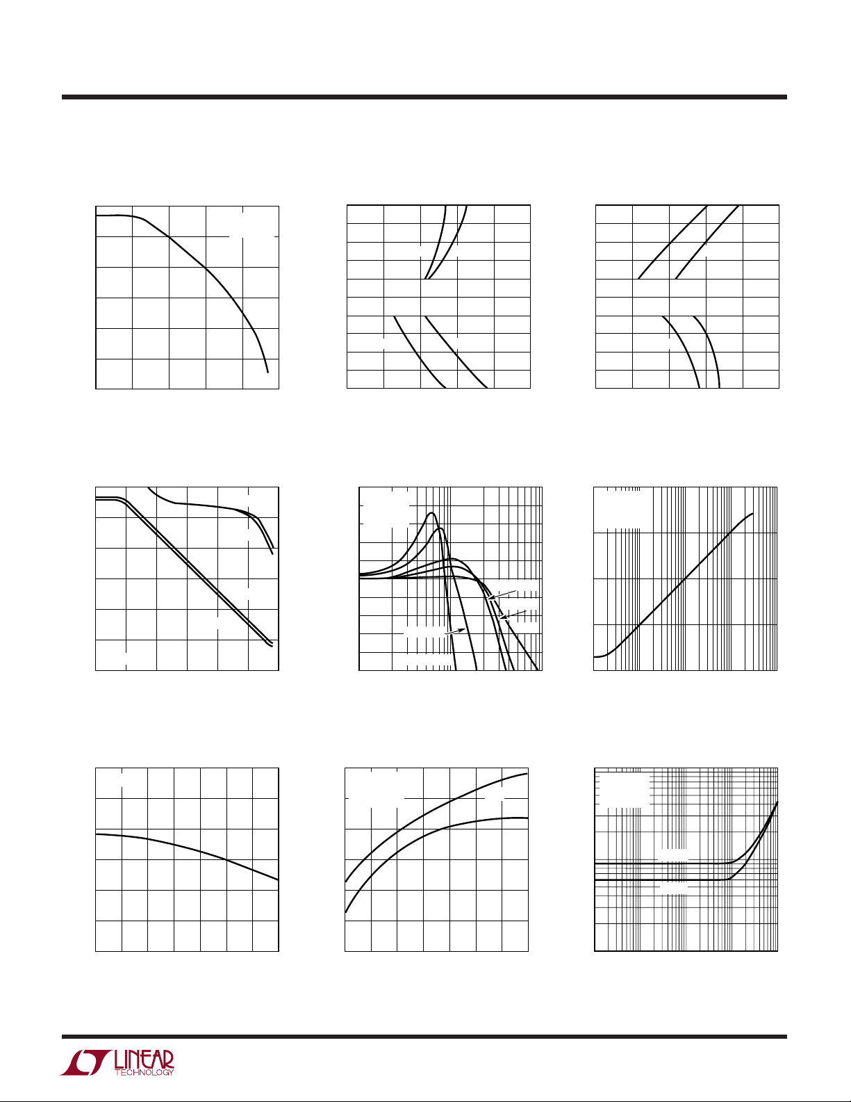
FREQUENCY (Hz)
100
0
POWER SUPPLY REJECTION RATIO (dB)
20
60
100
1k 100k 1M 100M
LT1220 • TPC09
40
80
10k 10M
+PSRR
VS = ±15V
T
A
= 25°C
–PSRR
W
U
TYPICAL PERFORMANCE CHARACTERISTICS
Input Common Mode Range
vs Supply Voltage
20
TA = 25°C
= 0.5mV
∆V
OS
15
10
5
MAGNITUDE OF INPUT VOLTAGE (V)
0
0
5101520
SUPPLY VOLTAGE (±V)
+V
–V
Output Voltage Swing
vs Resistive Load
30
TA = 25°C
= 30mV
∆V
)
P-P
OUTPUT VOLTAGE SWING (V
OS
25
20
±15V SUPPLIES
15
10
5
0
10
LOAD RESISTANCE (Ω)
±5V SUPPLIES
100 1k 10k
CM
CM
LT1220 • TPC01
LT1220 • TPC04
Supply Current vs Supply Voltage
and Temperature
9.0
TA = 25°C
8.5
8.0
SUPPLY CURRENT (mA)
7.5
7.0
0
5101520
SUPPLY VOLTAGE (±V)
Input Bias Current
vs Input Common Mode Voltage
500
TA = 25°C
400
= ±15V
V
S
300
200
100
0
–100
–200
INPUT BIAS CURRENT (nA)
–300
–400
–500
–10 –5 10
–15
INPUT COMMON MODE VOLTAGE (V)
+
I
B
–
I
B
05 15
LT1220 • TPC02
LT1220 • TPC05
Output Voltage Swing
vs Supply Voltage
20
TA = 25°C
R
= 500Ω
L
∆V
= 30mV
OS
15
+V
10
–V
SW
5
MAGNITUDE OF OUTPUT VOLATGE (V)
0
0
5101520
SUPPLY VOLTAGE (±V)
Open-Loop Gain
vs Resistive Load
110
TA = 25°C
100
VS = ±15V
90
80
OPEN-LOOP GAIN (dB)
70
60
10
100 1k 10k
LOAD RESISTANCE (Ω)
SW
LT1220 • TPC03
VS = ±5V
LT1220 • TPC06
Output Short-Circuit Current
vs Temperature
50
VS = ±5V
45
40
35
30
25
OUTPUT SHORT-CIRCUIT CURRENT (mA)
20
–50
4
025 75
–25 50 100 125
TEMPERATURE (°C)
LT1220 • TPC07
Input Noise Spectral Density
160
VS = ±15V
T
= 25°C
140
A
= 100
A
V
√
120
100
80
60
40
INPUT VOLTAGE NOISE (nV/ Hz)
20
0
10
100 1k 10k 100k
FREQUENCY (Hz)
Power Supply Rejection Ratio
vs Frequency
LT1220 • TPC08
Page 5
W
FREQUENCY (Hz)
0.1
OUTPUT IMPEDANCE (Ω)
1
10
100
10k 1M 10M 100M
LT1220 • TPC15
0.01
100k
VS = ±15V
T
A
= 25°C
A
V
= 1
U
TYPICAL PERFORMANCE CHARACTERISTICS
LT1220
Common Mode Rejection Ratio
vs Frequency
120
100
80
60
40
20
COMMON MODE REJECTION RATIO (dB)
0
10k 10M
1k
100k 1M 100M
FREQUENCY (Hz)
Voltage Gain and Phase
vs Frequency
100
80
60
40
20
VOLTAGE GAIN (dB)
0
= 25°C
T
A
–20
1k 100k 1M 100M
100
10k 10M
FREQUENCY (Hz)
VS = ±5V
VS = ±15V
= 25°C
T
A
LT1220 • TPC10
VS = ±15V
= ±5V
V
S
VS = ±15V
LT1220 • TPC13
10
8
6
4
2
0
–2
OUTPUT SWING (V)
–4
–6
–8
–10
100
80
PHASE MARGIN (DEG)
60
40
20
0
–20
–2
–4
VOLTAGE MAGNITUDE (dB)
–6
–8
–10
Output Swing and Error
vs Settling Time (Noninverting)
10mV
10mV
25
0
SETTLING TIME (ns)
1mV
1mV
75
50
100
LT1220 • TPC11
Frequency Response
vs Capacitive Load
10
VS = ±15V
8
= 25°C
T
A
= –1
A
V
6
4
2
0
C = 500pF
C = 1000pF
1
10 100
FREQUENCY (MHz)
C = 100pF
C = 50pF
LT1220 • TPC14
125
C = 0
Output Swing and Error
vs Settling Time (Inverting)
10
8
6
4
2
0
–2
OUTPUT SWING (V)
–4
–6
–8
–10
10mV
25
0
10mV
SETTLING TIME (ns)
1mV
75
50
Closed-Loop Output Impedance
vs Frequency
1mV
100
LT1220 • TPC12
125
Gain-Bandwidth vs Temperature
50
VS = ±15V
48
46
44
42
GAIN-BANDWIDTH (MHz)
40
38
–25 50 100 125
–50
025 75
TEMPERATURE (°C)
LT1220 • TPC16
Slew Rate vs Temperature
300
VS = ±15V
A
= –1
V
275
R
= RF = 1k
IN
250
–SR
225
200
SLEW RATE (V/µs)
175
150
–50
025 75
–25 50 100 125
TEMPERATURE (°C)
+SR
LT1220 • TPC24
Total Harmonic Distortion
vs Frequency
0.01
VS = ±15V
V
= 3V
O
RMS
RL = 500Ω
0.001
0.0001
TOTAL HARMONIC DISTORTION AND NOISE (%)
10 100
AV = –1
AV = 1
1k 10k 100k
FREQUENCY (Hz)
LT1220 • TPC18
5
Page 6
LT1220
W
U
TYPICAL PERFORMANCE CHARACTERISTICS
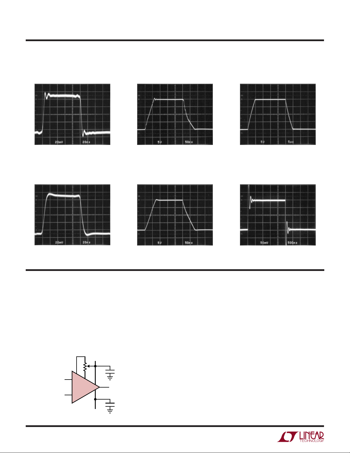
Large Signal, AV = 1Small Signal, AV = 1
Large Signal, AV = 1,
CL = 10,000pF
V
RG = 0
= ±15V
V
S
= 100mV
IN
f = 5MHz
Small Signal, AV = –1
V
RF = RG = 1k
= ±15V
V
S
= 100mV
IN
f = 5MHz
LT1220 • TPC19
LT1220 • TPC22
U
RG = 0
= ±15V
V
S
Large Signal, AV = –1
RF = RG = 1k
= ±15V
V
S
WUU
V
= 20V
IN
f = 2MHz
V
= 20V
IN
f = 2MHz
APPLICATIONS INFORMATION
The LT1220 may be inserted directly into HA2505/15/25,
HA2541/2/4, AD817, AD847, EL2020, EL2044 and LM6361
applications, provided that the nulling circuitry is removed.
The suggested nulling circuit for the LT1220 is shown in
the following figure.
Offset Nulling
+
V
5k
1
3
2
+
LT1220
–
8
7
4
–
V
0.1µF
6
0.1µF
LT1220 • AI01
LT1220 • TPC20
R
G
V
S
= 0
= ±15V
VIN = 10V
f = 20kHz
LT1220 • TPC21
Small Signal, AV = –1,
CL = 1,000pF
LT1220 • TPC23 LT1220 • TPC24
= RG = 1k
R
F
V
= ±15V
S
VIN = 200mV
f = 200kHz
Layout and Passive Components
The LT1220 amplifier is easy to apply and tolerant of less
than ideal layouts. For maximum performance (for example, fast settling time) use a ground plane, short lead
lengths and RF-quality bypass capacitors (0.01µF to 0.1µF).
For high driver current applications use low ESR bypass
capacitors (1µF to 10µF tantalum). Sockets should be
avoided when maximum frequency performance is required, although low profile sockets can provide reasonable performance up to 50MHz. For more details see
Design Note 50. Feedback resistors greater than 5k are not
recommended because a pole is formed with the input
capacitance which can cause peaking or oscillations.
6
Page 7
LT1220
U
WUU
APPLICATIONS INFORMATION
Input Considerations
Bias current cancellation circuitry is employed on the
inputs of the LT1220 so the input bias current and input
offset current have identical specifications. For this reason,
matching the impedance on the inputs to reduce bias
current errors is not necessary.
Capacitive Loading
The LT1220 is stable with capacitive loads. This is accomplished by sensing the load induced output pole and adding
compensation at the amplifier gain node. As the capacitive
load increases, both the bandwidth and phase margin
decrease. There will be peaking in the frequency domain as
shown in the curve of Frequency Response vs Capacitive
Load. The small-signal transient response will have more
overshoot as shown in the photo of the small-signal
response with 1000pF load. The large-signal response with
a 10,000pF load shows the output slew rate being limited
to 4V/µs by the short-circuit current. The LT1220 can drive
coaxial cable directly, but for best pulse fidelity a resistor of
value equal to the characteristic impedance of the cable
(i.e., 75Ω) should be placed in series with the output. The
other end of the cable should be terminated with the same
value resistor to ground.
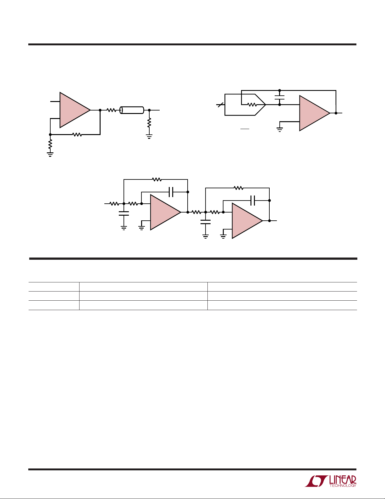
DAC Current-to-Voltage Amplifier
The high gain, low offset voltage, low input bias current,
and fast settling of the LT1220 make it particularly useful
as an I/V converter for current output DACs. A typical
application is shown with a 565A type, 12-bit, 2mA fullscale output current DAC. The 5k resistor around the
LT1220 is internal to the DAC and gives a 10V full-scale
output voltage. A 5pF capacitor in parallel with the feedback
resistor compensates for the DAC output capacitance and
improves settling. The output of the LT1220 settles to
1/2LSB (1.2mV) in less than 300ns. The accuracy of this
circuit is equal to:
V
= VOS + (IOS • 5kΩ) + (V
ERROR
OUT/AVOL
)
At room temperature the worst-case error is 3mV (1.2LSB).
Typically the error is 1.2mV (1/2LSB). Over the commercial
temperature range the worse-case error is 6mV (2.5LSB).
WW
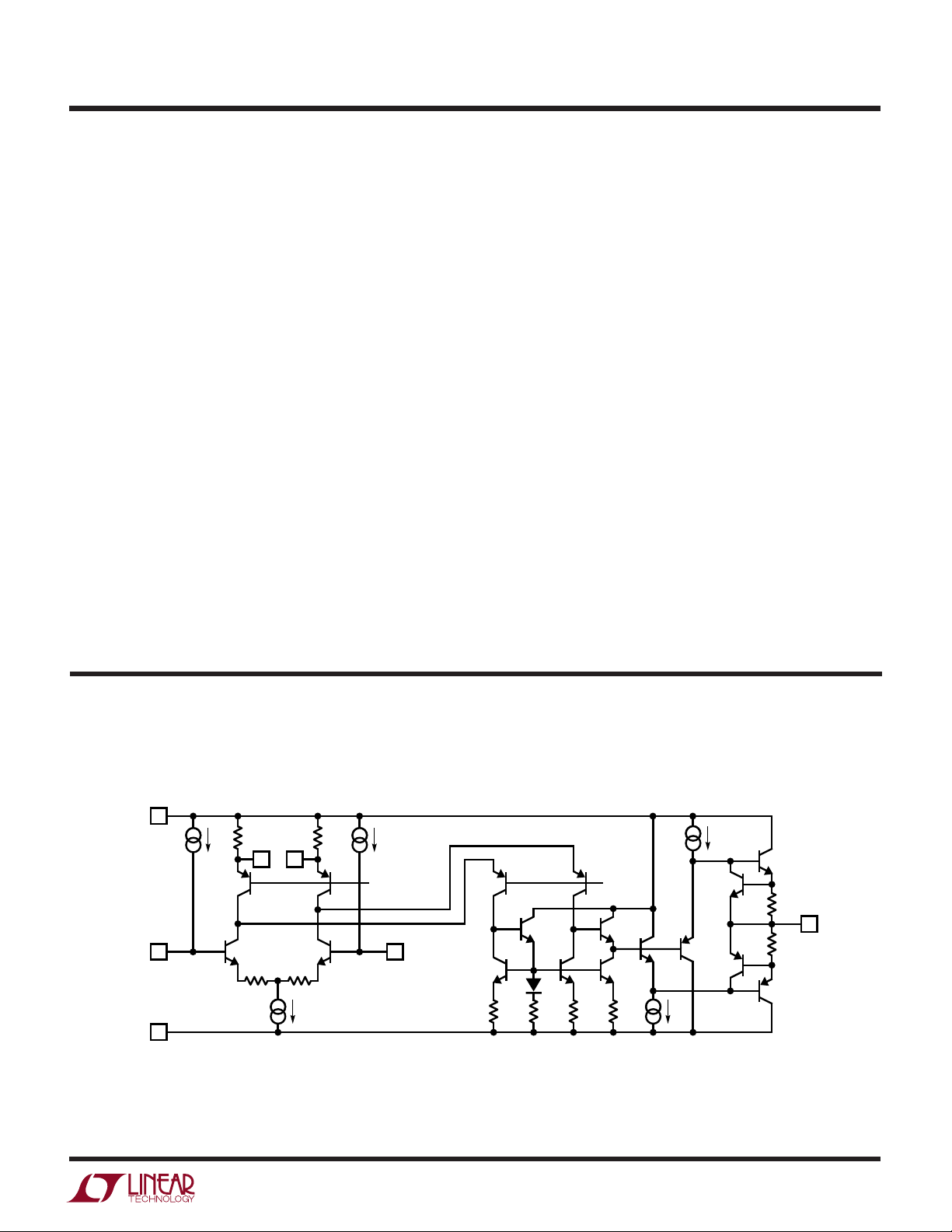
SI PLIFIED SCHE ATIC
+
7V
NULL
18
+IN 3
–
V
4
2
BIAS 2BIAS 1
6 OUT
–IN
LT1220 • SS
7
Page 8
LT1220
PACKAGE DESCRIPTIO
(1.016)
SEATING
PLANE
0.010 – 0.045*
(0.254 – 1.143)
U
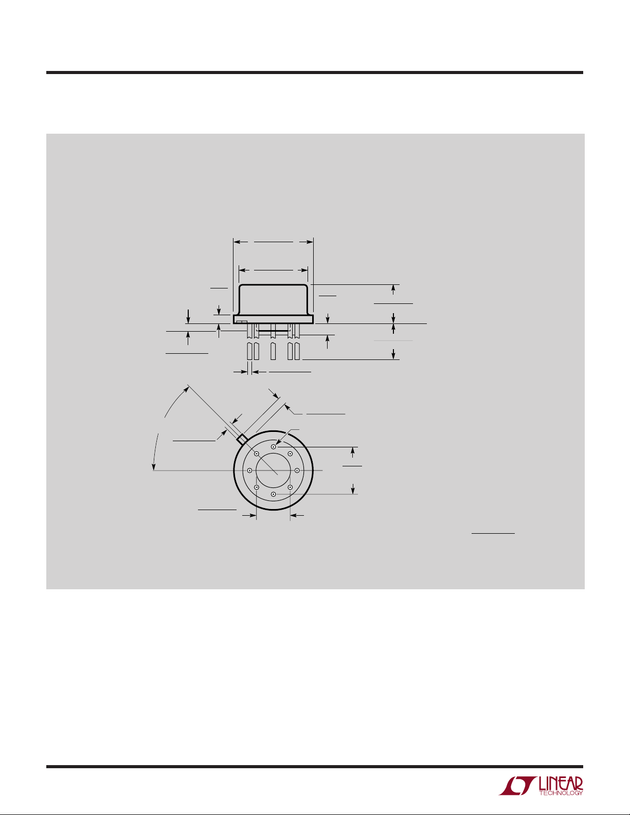
H Package
8-Lead TO-5 Metal Can (.200 Inch PCD)
(Reference LTC DWG # 05-08-1320)
0.335 – 0.370
(8.509 – 9.398)
DIA
0.305 – 0.335
0.040
MAX
(7.747 – 8.509)
0.016 – 0.021**
(0.406 – 0.533)
0.050
(1.270)
MAX
GAUGE
PLANE
0.165 – 0.185
(4.191 – 4.699)
0.500 – 0.750
(12.700 – 19.050)
REFERENCE
PLANE
45°TYP
0.028 – 0.034
(0.711 – 0.864)
0.110 – 0.160
(2.794 – 4.064)
INSULATING
STANDOFF
0.027 – 0.045
(0.686 – 1.143)
PIN 1
0.200
(5.080)
TYP
*
LEAD DIAMETER IS UNCONTROLLED BETWEEN THE REFERENCE PLANE
AND 0.045" BELOW THE REFERENCE PLANE
**
FOR SOLDER DIP LEAD FINISH, LEAD DIAMETER IS
OBSOLETE PACKAGE
0.016 – 0.024
(0.406 – 0.610)
H8(TO-5) 0.200 PCD 1197
8
Page 9
PACKAGE DESCRIPTIO
LT1220
U
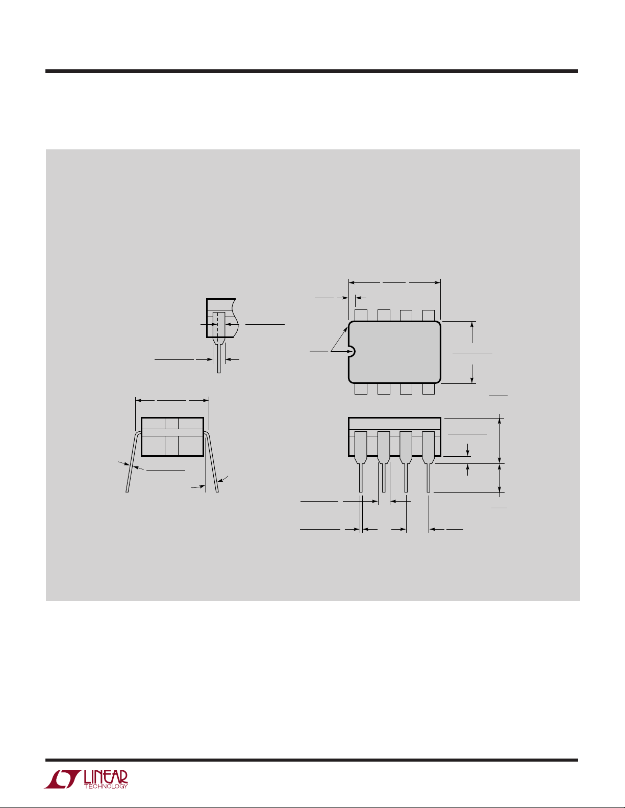
J8 Package
8-Lead CERDIP (Narrow .300 Inch, Hermetic)
(Reference LTC DWG # 05-08-1110)
CORNER LEADS OPTION
(4 PLCS)
0.023 – 0.045
(0.584 – 1.143)
HALF LEAD
0.045 – 0.068
(1.143 – 1.727)
FULL LEAD
OPTION
0.300 BSC
(0.762 BSC)
0.008 – 0.018
(0.203 – 0.457)
NOTE: LEAD DIMENSIONS APPLY TO SOLDER DIP/PLATE
OR TIN PLATE LEADS
0° – 15°
OPTION
OBSOLETE PACKAGE
0.005
(0.127)
MIN
0.025
(0.635)
RAD TYP
0.045 – 0.065
(1.143 – 1.651)
0.014 – 0.026
(0.360 – 0.660)
0.405
(10.287)
MAX
87
12
65
3
4
0.220 – 0.310
(5.588 – 7.874)
0.015 – 0.060
(0.381 – 1.524)
0.100
(2.54)
BSC
0.200
(5.080)
MAX
0.125
3.175
MIN
J8 1298
9
Page 10
LT1220
PACKAGE DESCRIPTIO
U
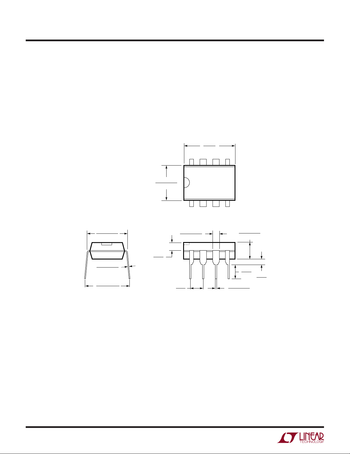
N8 Package
8-Lead PDIP (Narrow .300 Inch)
(Reference LTC DWG # 05-08-1510)
0.255 ± 0.015*
(6.477 ± 0.381)
0.400*
(10.160)
MAX
876
5
12
0.300 – 0.325
(7.620 – 8.255)
0.065
(1.651)
0.009 – 0.015
(0.229 – 0.381)
+0.035
0.325
–0.015
+0.889
8.255
()
–0.381
*THESE DIMENSIONS DO NOT INCLUDE MOLD FLASH OR PROTRUSIONS.
MOLD FLASH OR PROTRUSIONS SHALL NOT EXCEED 0.010 INCH (0.254mm)
TYP
0.045 – 0.065
(1.143 – 1.651)
0.100
(2.54)
BSC
3
4
0.130 ± 0.005
(3.302 ± 0.127)
0.125
(3.175)
MIN
0.018 ± 0.003
(0.457 ± 0.076)
0.020
(0.508)
MIN
N8 1098
10
Page 11
PACKAGE DESCRIPTIO
U
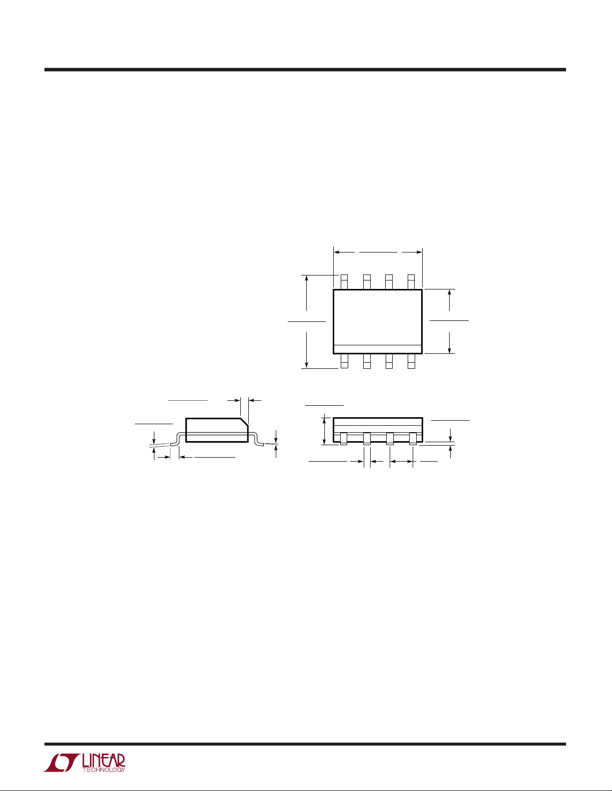
S8 Package
8-Lead Plastic Small Outline (Narrow .150 Inch)
(Reference LTC DWG # 05-08-1610)
0.189 – 0.197*
(4.801 – 5.004)
7
8
6
LT1220
5
0.228 – 0.244
(5.791 – 6.197)
0.010 – 0.020
(0.254 – 0.508)
0.008 – 0.010
(0.203 – 0.254)
*
DIMENSION DOES NOT INCLUDE MOLD FLASH. MOLD FLASH
SHALL NOT EXCEED 0.006" (0.152mm) PER SIDE
**
DIMENSION DOES NOT INCLUDE INTERLEAD FLASH. INTERLEAD
FLASH SHALL NOT EXCEED 0.010" (0.254mm) PER SIDE
×
°
45
0.016 – 0.050
(0.406 – 1.270)
0°– 8° TYP
0.053 – 0.069
(1.346 – 1.752)
0.014 – 0.019
(0.355 – 0.483)
TYP
0.150 – 0.157**
(3.810 – 3.988)
SO8 1298
1
3
2
4
0.004 – 0.010
(0.101 – 0.254)
0.050
(1.270)
BSC
Information furnished by Linear Technology Corporation is believed to be accurate and reliable.
However, no responsibility is assumed for its use. Linear Technology Corporation makes no representation that the interconnection of its circuits as described herein will not infringe on existing patent rights.
11
Page 12
LT1220
LT1220 • TA04
+
–
V
OUT
5k
LT1220
5pF
565A TYPE
DAC
INPUTS
12
V
OS
+ IOS (5kΩ) + < 1/2LSB
V
OUT
A
VOL
U
TYPICAL APPLICATIONS N
Cable Driver
V
+
IN
LT1220
–
1k
1k
75Ω
75Ω CABLE
V
75Ω
LT1220 • TA03
OUT
DAC Current-to-Voltage Converter
1MHz, 4th Order Butterworth Filter
909Ω
47pF
2.67k
909Ω
V
IN
220pF
–
LT1220
+
2.21k1.1k
470pF
1.1k
–
LT1220
22pF
V
OUT
+
LT1220 • TA05
RELATED PARTS
PART NUMBER DESCRIPTION COMMENTS
LT1221 150MHz, 250V/µs Amplifier AV ≥ 4 Version of the LT1220
LT1222 500MHz, 200V/µs Amplifier AV ≥ 10 Version of the LT1220
12
Linear Technology Corporation
1630 McCarthy Blvd., Milpitas, CA 95035-7417
(408) 432-1900 ● FAX: (408) 434-0507
●
www.linear.com
1220fb LT/CP 0801 1.5K REV B • PRINTED IN USA
LINEAR TECHNOLOGY CORPORATION 1991
 Loading...