

Page 1
LT1217
FREQUENCY (Hz)
100k
–20
AMPLIFIER VOLTAGE GAIN (dB)
10
40
50
60
1M 10M 100M
LT1217 • TA02
–10
0
20
30
RG = 30Ω
RG = 100Ω
RG = 330Ω
RG = 1.3k
RG = ∞
VS = ±15V
R
F
= 3k
R
L
= 100Ω
Low Power 10MHz
Current Feedback Amplifier
EATU
F
■
1mA Quiescent Current
■
50mA Output Current (Minimum)
■
10MHz Bandwidth
■
500V/µs Slew Rate
■
280ns Settling Time to 0.1%
■
Wide Supply Range, ±5V to ±15V
■
1mV Input Offset Voltage
■
100nA Input Bias Current
■
100MΩ Input Resistance
PPLICATI
A
■
Video Amplifiers
■
Buffers
■
IF and RF Amplification
■
Cable Drivers
■
8, 10, 12-Bit Data Acquisition Systems
RE
S
O
U
S
DUESCRIPTIO
The LT1217 is a 10MHz current feedback amplifier with DC
characteristics better than many voltage feedback amplifiers. This versatile amplifier is fast, 280ns settling to 0.1%
for a 10V step thanks to its 500V/µs slew rate. The LT1217
is manufactured on Linear Technology’s proprietary
complementary bipolar process resulting in a low 1mA
quiescent current. To reduce power dissipation further,
the LT1217 can be turned off, eliminating the load current
and dropping the supply current to 350µA.
The LT1217 is excellent for driving cables and other low
impedance loads thanks to a minimum output drive current of 50mA. Operating on any supplies from ±5V to ±15V
allows the LT1217 to be used in almost any system. Like
other current feedback amplifiers, the LT1217 has high
gain bandwidth at high gains. The bandwidth is over 1MHz
at a gain of 100.
The LT1217 comes in the industry standard pinout and
can upgrade the performance of many older products.
CA
A
PPLICATITYPI
L
V
+
IN
LT1217
–
R
3k
RG
3k
R
F
AV = 1 +
R
G
AT AMPLIFIER OUTPUT.
6dB LESS AT V
U
O
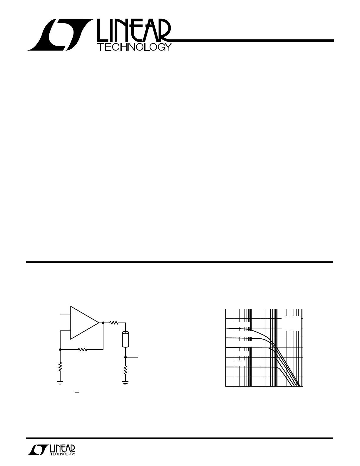
Cable Driver Voltage Gain vs Frequency
75Ω
F
.
OUT
75Ω
CABLE
75Ω
LT1217 • TA01
V
OUT
1
Page 2
LT1217
WU
U
PACKAGE
/
O
RDER I FOR ATIO
W
O
A
LUTEXI T
S
Supply Voltage ...................................................... ±18V
Input Current ...................................................... ±10mA
Input Voltage ............................ Equal to Supply Voltage
Output Short Circuit Duration (Note 1) .........Continuous
Operating Temperature Range ..................... 0°C to 70°C
Storage Temperature Range ................. –65°C to 150°C
Junction Temperature........................................... 150°C
Lead Temperature (Soldering, 10 sec.)................. 300°C
LECTRICAL C CHARA TERIST
E
SYMBOL PARAMETER CONDITIONS MIN TYP MAX UNITS
V
OS
I
IN+
I
IN–
e
n
i
n
R
IN
C
IN
CMRR Common Mode Rejection Ratio V
PSRR Power Supply Rejection Ratio VS = ±4.5V to ±18V ● 68 76 dB
A
V
R
OL
V
OUT
I
OUT
SR Slew Rate (Note 2, 3) RF = 3k, RG = 3k ● 100 500 V/µs
BW Bandwidth RF = 3k, RG = 3k, V
t
r
t
PD
t
s
I
S
Input Offset Voltage V
Non-Inverting Input Current V
Inverting Input Current V
Input Noise Voltage Density f = 1kHz, RF = 1k, RG = 10Ω 6.5 nV/√Hz
Input Noise Current Density f = 1kHz, RF = 1k, RG = 10Ω 0.7 pA/√Hz
Input Resistance V
Input Capacitance 1.5 pF
Input Voltage Range ● ±10 ±12 V
Inverting Input Current Common Mode Rejection V
Non-Inverting Input Current Power Supply Rejection VS = ±4.5V to ±18V ● 2 20 nA/V
Inverting Input Current Power Supply Rejection VS = ±4.5V to ±18V ● 10 50 nA/V
Large Signal Voltage Gain R
Transresistance, ∆V
Output Swing R
Output Current R
Rise Time, Fall Time (Note 3) RF = 3k, RG = 3k, V
Propagation Delay RF = 3k, RG = 3k, V
Overshoot RF = 3k, RG = 3k, V
Settling Time, 0.1% RF = 3k, RG = 3k, V
Supply Current VIN = 0V ● 12 mA
Supply Current, Shutdown Pin 8 Current = 50µA ● 350 1000 µA
A
OUT
/∆I
WUW
IN–
ARB
U
G
S
I
TOP VIEW
1NULL
2
–IN
+IN
3
–
V
N8 PACKAGE
8-LEAD PLASTIC DIP
ICS
VS = ±15V, TA = 0°C to 70°C unless otherwise noted.
= 0V ● ±1 ±3mV
CM
= 0V ● ±100 ±500 nA
CM
= 0V ● ±100 ±500 nA
CM
= ±10V ● 20 100 MΩ
IN
= ±10V ● 60 66 dB
CM
= ±10V ● 5 20 nA/V
CM
= 2k, V
LOAD
= 400Ω, V
R
LOAD
R
= 2k, V
LOAD
= 400Ω, V
R
LOAD
= 2k ● ±12 ±13 V
LOAD
= 200Ω ● ±10 V
R
LOAD
= 0Ω ● 50 100 mA
LOAD
= ±10V ● 90 105 dB
OUT
= ±10V ● 70 dB
OUT
= ±10V ● 545 MΩ
OUT
= ±10V ● 1.5 MΩ
OUT
= 100mV 10 MHz
OUT
= 1V ● 30 40 ns
OUT
= 1V 25 ns
OUT
= 1V 5 %
OUT
= 10V 280 ns
OUT
8
7
6
54
S8 PACKAGE
8-LEAD PLASTIC SOIC
SHUTDOWN
+
V
OUT
NULL
LT1217 • POI01
ORDER PART
NUMBER
LT1217CN8
LT1217CS8
S8 PART MARKING
1217
The ● denotes specifications which apply over the operating temperature
range.
Note 1: A heat sink may be required.
2
Note 2: Non-Inverting operation, V
Note 3: AC parameters are 100% tested on the plastic DIP packaged parts
(N suffix), and are sample tested on every lot of the SO packaged parts
(S suffix).
= ±10V, measured at ±5V.
OUT
Page 3
UW
SUPPLY VOLTAGE (±V)
0
0
–3dB BANDWIDTH (MHz)
0.5
1.0
1.5
2.0
2.5
4 8 14 18
LT1217 • TPC09
2 6 10 12 16
RF = 250Ω
RF = 5.1k
RF = 1k
SUPPLY VOLTAGE (±V)
0
0
–3dB BANDWIDTH (MHz)
5
10
15
20
25
30
4 8 14 18
LT1217 • TPC03
2 6 10 12 16
RF = 1k
RF = 2k
RF = 3k
RF = 5.1k
PEAKING ≤ 0.5dB
PEAKING ≤ 5dB
SUPPLY VOLTAGE (±V)
0
0
–3dB BANDWIDTH (MHz)
4
6
12
16
18
20
4 8 14 18
LT1217 • TPC06
2 6 10 12 16
RF = 5.1k
14
10
8
2
PEAKING ≤ 0.5dB
PEAKING ≤ 5dB
RF = 2k
RF = 3k
RF = 1k
R
F
= 750Ω
Y
PICA
8
7
6
5
4
3
2
1
VOLTAGE GAIN (dB)
0
–1
–2
0.01
22
21
20
19
18
17
16
15
VOLTAGE GAIN (dB)
14
13
12
0.01
LPER
F
O
R
AT
CCHARA TERIST
E
C
ICS
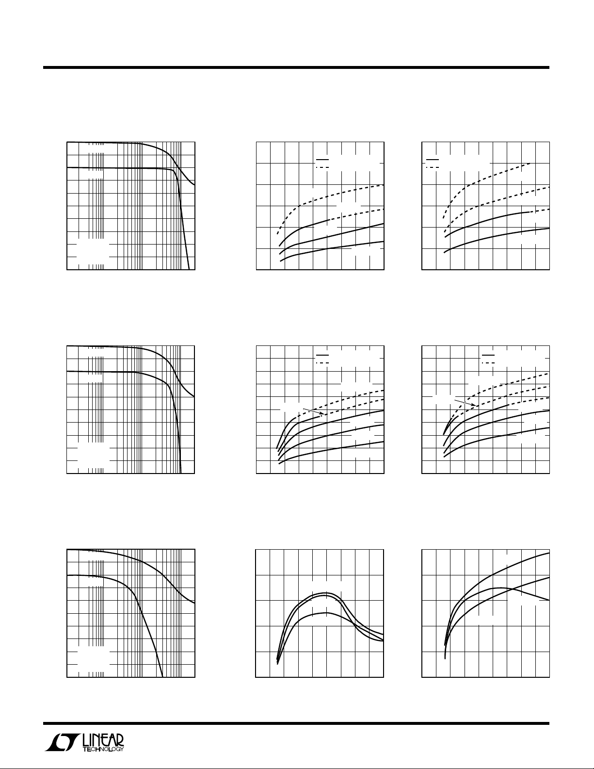
Voltage Gain and Phase vs –3dB Bandwidth vs Supply –3dB Bandwidth vs Supply
Frequency, Gain = 6dB Voltage, Gain = 2, RL = 100Ω Voltage, Gain = 2, RL = 1kΩ
PHASE
GAIN
VS = ±15V
= 100Ω
R
L
R
= 3k
F
0.1 1.0 10
FREQUENCY (MHz)
0
45
90
135
180
225
LT1217 • TPC01
30
25
PHASE SHIFT (DEGREES)
20
15
10
–3dB BANDWIDTH (MHz)
5
0
2 6 10 12 16
0
PEAKING ≤ 0.5dB
PEAKING ≤ 5dB
RF = 1k
RF = 2k
RF = 3k
RF = 5.1k
4 8 14 18
SUPPLY VOLTAGE (±V)
LT1217 • TPC02
Voltage Gain and Phase vs –3dB Bandwidth vs Supply –3dB Bandwidth vs Supply
Frequency, Gain = 20dB Voltage, Gain = 10, RL = 100Ω Voltage, Gain = 10, RL = 1kΩ
PHASE
GAIN
VS = ±15V
= 100Ω
R
L
R
= 3k
F
0.1 1.0 10
FREQUENCY (MHz)
0
45
90
135
180
225
LT1217 • TPC04
20
18
16
PHASE SHIFT (DEGREES)
14
12
10
8
6
–3dB BANDWIDTH (MHz)
4
2
0
2 6 10 12 16
0
PEAKING ≤ 0.5dB
PEAKING ≤ 5dB
= 750Ω
R
F
RF = 1k
RF = 2k
RF = 3k
RF = 5.1k
4 8 14 18
SUPPLY VOLTAGE (±V)
LT1217 • TPC05
LT1217
Voltage Gain and Phase vs –3dB Bandwidth vs Supply –3dB Bandwidth vs Supply
Frequency, Gain = 40dB Voltage, Gain = 100, RL = 100Ω Voltage, Gain = 100, RL = 1kΩ
42
41
40
39
38
37
36
35
VOLTAGE GAIN (dB)
34
33
32
0.01
PHASE
GAIN
VS = ±15V
R
L
R
= 3k
F
= 100Ω
0.1 1.0 10
FREQUENCY (MHz)
LT1217 • TPC07
0
45
90
135
180
225
2.5
2.0
PHASE SHIFT (DEGREES)
1.5
1.0
–3dB BANDWIDTH (MHz)
0.5
RF = 250Ω
RF = 1k
RF = 5.1k
0
2 6 10 12 16
4 8 14 18
0
SUPPLY VOLTAGE (±V)
LT1217 • TPC08
3
Page 4

LT1217
FREQUENCY (MHz)
0.01
0.1
RESISTANCE (Ω)
1
100
1000
10000
0.1 1 10
LT1217 • TPC18
VS = ±15V
R
F
= RG = 3k
10
NORMAL
SHUTDOWN
(PIN 8 AT GND)
FREQUENCY (MHz)
0.1
–60
DISTORTION (dBc)
–50
–40
–30
–20
110
LT1217 • TPC12
VS = ±15V
R
L
= 100Ω
V
O
= 2Vpp
R
F
= 3k
A
V
= 10dB
3RD
2ND
UW
Y
PICA
10000
1000
100
CAPACITIVE LOAD (pF)
10
+
V
–1.0
–2.0
–3.0
3.0
2.0
COMMON MODE RANGE (V)
1.0
–
V
–50
LPER
F
O
R
AT
CCHARA TERIST
E
C
ICS
Maximum Capacitive Load vs Total Harmonic Distortion vs 2nd and 3rd Harmonic
Feedback Resistor Frequency Distortion vs Frequency
AV = 2
= 1k
R
L
PEAKING ≤ 5dB
VS = ±5V
23 56 89
1
4710
FEEDBACK RESISTOR (kΩ)
VS = ±15V
LT1217 • TPC10
0.1
VS = ±15V
= 400Ω
R
L
= RG = 3kΩ
R
F
0.01
TOTAL HARMONIC DISTORTION (%)
0.001
10 1000 10000 100000
100
VO = 7V
FREQUENCY (Hz)
RMS
VO = 2V
RMS
LT1217 • TPC11
Input Common Mode Limit vs Output Saturation Voltage vs Output Short Circuit Current vs
Temperature Temperature Temperature
V+ = +5V TO +18V
V– = –5V TO –18V
0 25 75 125
–25 50 100
PACKAGE TEMPERATURE (°C)
LT1217 • TPC13
+
V
–0.5
–1.0
–1.5
–2.0
2.0
1.5
1.0
OUTPUT SATURATION VOLTAGE (V)
0.5
–
V
–25 50 100
–50
RL = ∞
±5V ≤ V
≤ ±18V
S
0 25 75 125
PACKAGE TEMPERATURE (°C)
LT1217 • TPC14
120
110
100
90
80
70
60
50
OUTPUT SHORT CIRCUIT CURRENT (mA)
40
–50
0 25 75 125
–25 50 100
PACKAGE TEMPERATURE (°C)
LT1217 • TPC15
SPOT NOISE (nV/√Hz OR pA/√Hz)
4
Spot Noise Voltage and Current vs Power Supply Rejection vs Output Impedance vs
Frequency Frequency Frequency
100
i
10
e
n
1
0.1
0.01 1 10 100
0.1
FREQUENCY (kHz)
n–
i
n+
LT1217 • TPC16
70
60
50
40
30
20
VS = ±15V
POWER SUPPLY REJECTION (dB)
= 100Ω
R
10
L
= RG =3k
R
F
0
0.01
POSITIVE
NEGATIVE
0.1 1 10
FREQUENCY (MHz)
LT1217 • TPC17
Page 5

LT1217
SUPPLY VOLTAGE (±V)
0
0.0
SUPPLY CURRENT (mA)
0.2
0.4
0.6
1.0
1.2
1.4
4 10 14 18
LT1217 • TPC21
2681216
0.8
T = 25°C, 125°C
T = –55°C
T = 25°C
T = 125°C
SHUTDOWN
PIN 8 AT GND
T = –55°C
UW
Y
PICA
10
8
6
4
2
0
–2
OUTPUT STEP (V)
–4
–6
–8
–10
LPER
Settling Time to 10mV vs Settling Time to 1mV vs
Output Step Output Step Supply Current vs Supply Voltage
VS = ±15V
= RG = 3k
R
F
50 200
0
INVERTING
INVERTING
100 150 250 300
SETTLING TIME (ns)
R
F
O
NON-INVERTING
NON-INVERTING
AT
LT1217 • TPC19
CCHARA TERIST
E
C
10
VS = ±15V
8
= RG = 3k
R
F
6
4
2
0
–2
OUTPUT STEP (V)
–4
–6
–8
–10
0
NON-INVERTING
100
ICS
INVERTING
NON-INVERTING
INVERTING
300
200 400 500
SETTLING TIME (ns)
LT1217 • TPC20
PPLICATI
A
Current Feedback Basics
The small signal bandwidth of the LT1217, like all current
feedback amplifiers, isn’t a straight inverse function of the
closed loop gain. This is because the feedback resistors
determine the amount of current driving the amplifier’s
internal compensation capacitor. In fact, the amplifier’s
feedback resistor (RF) from output to inverting input
works with internal junction capacitances of the LT1217 to
set the closed loop bandwidth.
Even though the gain set resistor (RG) from inverting input
to ground works with RF to set the voltage gain just like it
does in a voltage feedback op amp, the closed loop
bandwidth does not change. This is because the equivalent
gain bandwidth product of the current feedback amplifier
is set by the Thevenin equivalent resistance at the inverting
input and the internal compensation capacitor. By keeping
RF constant and changing the gain with RG, the Thevenin
resistance changes by the same amount as the change in
gain. As a result, the net closed loop bandwidth of the
LT1217 remains the same for various closed loop gains.
The curve on the first page shows the LT1217 voltage gain
versus frequency while driving 100Ω, for five gain settings
from 1 to 100. The feedback resistor is a constant 3k and
the gain resistor is varied from infinity to 30Ω. Second
order effects reduce the bandwidth somewhat at the
higher gain settings.
U
O
S
WU
I FOR ATIO
U
Feedback Resistor Selection
The small signal bandwidth of the LT1217 is set by the
external feedback resistors and the internal junction capacitors. As a result, the bandwidth is a function of the
supply voltage, the value of the feedback resistor, the
closed loop gain and load resistor. The characteristic
curves of bandwidth versus supply voltage are done with
a heavy load (100Ω) and a light load (1kΩ) to show the
effect of loading. These graphs also show the family of
curves that result from various values of the feedback
resistor. These curves use a solid line when the response
has less than 0.5dB of peaking and a dashed line when the
response has 0.5dB to 5dB of peaking. The curves stop
where the response has more than 5dB of peaking.
At a gain of two, on ±15V supplies with a 3kΩ feedback
resistor, the bandwidth into a light load is 13.5MHz with a
little peaking, but into a heavy load the bandwidth is
10MHz with no peaking. At very high closed loop gains, the
bandwidth is limited by the gain bandwidth product of
about 100MHz. The curves show that the bandwidth at a
closed loop gain of 100 is about 1MHz.
Capacitance on the Inverting Input
Current feedback amplifiers want resistive feedback from
the output to the inverting input for stable operation. Take
5
Page 6

LT1217
PPLICATI
A
U
O
S
I FOR ATIO
WU
U
care to minimize the stray capacitance between the output
and the inverting input. Capacitance on the inverting input
to ground will cause peaking in the frequency response
(and overshoot in the transient response), but it does not
degrade the stability of the amplifier. The amount of
capacitance that is necessary to cause peaking is a func-
tion of the closed loop gain taken.
The higher the gain, the more capacitance is required to
cause peaking. We can add capacitance from the inverting
input to ground to increase the bandwidth in high gain
applications. For example, in this gain of 100 application,
the bandwidth can be increased from 1MHz to 2MHz by
adding a 2200pF capacitor.
V
IN
C
G
Boosting Bandwidth of High Gain Amplifier with
Capacitance on Inverting Input
45
44
43
42
41
40
GAIN (dB)
39
38
37
36
35
100k
+
LT1217
–
R
G
30Ω
CG = 2200pF
CG = 0
FREQUENCY (Hz)
R
F
3k
LT1229 • TA03
CG = 4700pF
1M 10M
LT1217 • TA04
V
OUT
Capacitive Loads
The LT1217 can be isolated from capacitive loads with a
small resistor (10Ω to 20Ω) or it can drive the capacitive
load directly if the feedback resistor is increased. Both
techniques lower the amplifier’s bandwidth about the
same amount. The advantage of resistive isolation is that
the bandwidth is only reduced when the capacitive load is
present. The disadvantage of resistor isolation is that
resistive loading causes gain errors. Because the DC
accuracy is not degraded with resistive loading, the desired way of driving capacitive loads, such as flash
converters, is to increase the feedback resistor. The Maximum Capacitive Load versus Feedback Resistor curve
shows the value of feedback resistor and capacitive load
that gives 5dB of peaking. For less peaking, use a larger
feedback resistor.
Power Supplies
The LT1217 may be operated with single or split supplies
as low as ±4.5V (9V total) to as high as ±18V (36V total).
It is not necessary to use equal value split supplies,
however, the offset voltage will degrade about 350µV per
volt of mismatch. The internal compensation capacitor
decreases with increasing supply voltage. The –3dB Bandwidth versus Supply Voltage curves show how this affects
the bandwidth for various feedback resistors. Generally,
the bandwidth at ±5V supplies is about half the value it is
at ±15V supplies for a given feedback resistor.
The LT1217 is very stable even with minimal supply
bypassing, however, the transient response will suffer if
the supply rings. It is recommended for good slew rate and
settling time that 4.7µF tantalum capacitors be placed
within 0.5 inches of the supply pins.
Input Range
The non-inverting input of the LT1217 looks like a 100MΩ
resistor in parallel with a 3pF capacitor until the common
mode range is exceeded. The input impedance drops
somewhat and the input current rises to about 10µA when
the input comes too close to the supplies. Eventually,
when the input exceeds the supply by one diode drop, the
base collector junction of the input transistor forward
biases and the input current rises dramatically. The input
current should be limited to 10mA when exceeding the
supplies. The amplifier will recover quickly when the input
is returned to its normal common mode range unless the
input was over 500mV beyond the supplies, then it will
take an extra 100ns.
6
Page 7

LT1217
U
O
PPLICATI
A
Offset Adjust
Output offset voltage is equal to the input offset voltage
times the gain plus the inverting input bias current times
the feedback resistor. The LT1217 output offset voltage
can be nulled by pulling approximately 30µA from pin 1 or
5. The easy way to do this is to use a 100kΩ pot between
pin 1 and 5 with a 430kΩ resistor from the wiper to ground
for 15V supply applications. Use a 110k resistor when
operating on a 5V supply.
Shutdown
Pin 8 activates a shutdown control function. Pulling more
than 50µA from pin 8 drops the supply current to less than
350µA, and puts the output into a high impedance state.
The easy way to force shutdown is to ground pin 8, using
an open collector (drain) logic stage. An internal resistor
limits current, allowing direct interfacing with no addi-
tional parts. When pin 8 is open, the LT1217 operates
normally.
S
I FOR ATIO
WU
U
Large Signal Response, AV = 2, RF = RG = 3k,
Slew Rate 500V/µs
Large Signal Response, AV = –2, RF = 3k, RG = 1.5k,
Slew Rate 850V/µs
Slew Rate
The slew rate of a current feedback amplifier is not
independent of the amplifier gain configuration the way it
is in a traditional op amp. This is because the input stage
and the output stage both have slew rate limitations.
Inverting amplifiers do not slew the input and are therefore
limited only by the output stage. High gain, non-inverting
amplifiers are similar. The input stage slew rate of the
LT1217 is about 50V/µs before it becomes non-linear and
is enhanced by the normally reverse biased emitters on the
input transistors. The output slew rate depends on the size
of the feedback resistors. The output slew rate is about
850V/µs with a 3k feedback resistor and drops propor-
tionally for larger values. The photos show the LT1217
with a 20V peak-to-peak output swing for three different
gain configurations.
Settling Time
The characteristic curves show that the LT1217 settles to
within 10mV of final value in less than 300ns for any output
step up to 10V. Settling to 1mV of final value takes less
than 500ns.
Large Signal Response, AV = 10, RF = 3k, RG = 330Ω,
Slew Rate 150V/µs
Information furnished by Linear Technology Corporation is believed to be accurate and reliable.
However, no responsibility is assumed for its use. Linear Technology Corporation makes no representation that the interconnection of its circuits as described herein will not infringe on existing patent rights.
7
Page 8

LT1217
W
SPL
I
IIFED S
CH
E
W
A
C
TI
7
90k
5
BIAS
60k
8
3
BIAS
2
1
6
PACKAGEDESCRIPTI
N8 Package
8-Lead Plastic DIP
T
J MAX
150°C 100°C/W
S8 Package
8-Lead Plastic SOIC
T
J MAX
150°C 150°C/W
θ
JA
θ
JA
0°– 8° TYP
U
O
Dimensions in inches (millimeters) unless otherwise noted.
0.300 – 0.320
(7.620 – 8.128)
0.009 - 0.015
(0.229 - 0.381)
+0.025
0.325
–0.015
+0.635
8.255
()
–0.381
0.010 – 0.020
(0.254 – 0.508)
0.016 – 0.050
0.406 – 1.270
× 45°
0.008 – 0.010
(0.203 – 0.254)
0.045 – 0.065
(1.143 – 1.651)
0.065
(1.651)
TYP
0.045 ± 0.015
(1.143 ± 0.381)
0.100 ± 0.010
(2.540 ± 0.254)
0.053 – 0.069
(1.346 – 1.753)
0.014 – 0.019
(0.356 – 0.483)
0.130 ± 0.005
(3.302 ± 0.127)
(0.457 ± 0.076)
0.004 – 0.010
(0.102 – 0.254)
0.050
(1.270)
BSC
0.125
(3.175)
MIN
0.018 ± 0.003
LT1217 • TA08
0.020
(0.508)
MIN
0.228 – 0.244
(5.791 – 6.198)
4
0.400
(10.160)
MAX
8
76
1234
8
1
5
0.189 – 0.197
(4.801 – 5.004)
7
6
3
2
0.250 ± 0.010
(6.350 ± 0.254)
N8 1291
5
0.150 – 0.157
(3.810 – 3.988)
4
S8 1291
8
Linear Technology Corporation
1630 McCarthy Blvd., Milpitas, CA 95035-7487
(408) 432-1900
●
FAX
: (408) 434-0507
●
TELEX
: 499-3977
BA/GP 0192 10K REV 0
LINEAR TECHNOLOGY CORPORATION 1992
 Loading...