

Page 1
FEATURES
■
Slew Rate: 50V/µs Typ
■
Gain-Bandwidth Product: 23MHz Typ
■
Fast Settling to 0.01%
2V Step to 200µV: 250ns Typ
10V Step to 1mV: 480ns Typ
■
Excellent DC Precision in All Packages
Input Offset Voltage: 450µV Max
Input Offset Voltage Drift: 10µV/°C Max
Input Offset Current: 120nA Max
Input Bias Current: 600nA Max
Open-Loop Gain: 1000V/mV Min
■
Single Supply Operation
Input Voltage Range Includes Ground
Output Swings to Ground While Sinking Current
■
Low Input Noise Voltage: 12.5nV/√Hz Typ
■
Low Input Noise Current: 0.5pA/√Hz Typ
■
Specified on 3.3V, 5V and ±15V
■
Large Output Drive Current: 30mA Min
■
Low Supply Current per Amplifier: 6.6mA Max
■
Dual in 8-Pin DIP and SO-8
■
Quad in 14-Pin DIP and NARROW SO-16
Note: For applications requiring less slew rate, see the LT1211/LT1212 and
LT1213/LT1214 data sheets.
LT1215/LT1216
23MHz, 50V/µs, Single Supply
Dual and Quad
Precision Op Amps
U
DESCRIPTIO
The LT®1215 is a dual, single supply precision op amp with
a 23MHz gain-bandwidth product and a 50V/µs slew rate.
The LT1216 is a quad version of the same amplifier. The
DC precision of the LT1215/LT1216 eliminates trims in
most systems while providing high frequency performance not usually found in single supply amplifiers.
The LT1215/LT1216 will operate on any supply greater
than 2.5V and less than 36V total. These amplifiers are
specified on single 3.3V, single 5V and ±15V supplies, and
only require 5mA of quiescent supply current per amplifier. The inputs can be driven beyond the supplies without
damage or phase reversal of the output. The minimum
output drive is 30mA, ideal for driving low impedance
loads.
U
APPLICATIO S
■
2.5V Full-Scale 12-Bit Systems: VOS ≤ 0.75 LSB
■
10V Full-Scale 16-Bit Systems: VOS ≤ 3 LSB
■
Active Filters
■
Photo Diode Amplifiers
■
DAC Current to Voltage Amplifiers
■
Battery-Powered Systems
, LTC and LT are registered trademarks of Linear Technology Corporation.
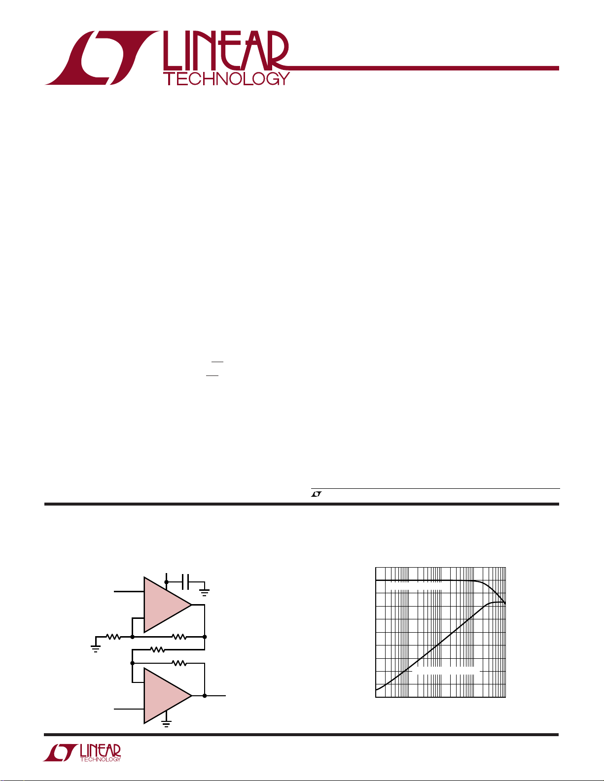
TYPICAL APPLICATIO
Single Supply Instrumentation Amplifier
5V
0.1µF
–
V
IN
V
IN
1020Ω
+
+
LT1215
–
113Ω
–
LT1215
+
1/2
113Ω
1020Ω
1/2
U
NOTE:
0.1% RESISTORS GIVE CMRR ≥ 68dB.
GAIN IS 10.0V/V.
COMMON MODE INPUT RANGE
IS FROM 0.3V TO 3.0V.
BANDWIDTH IS 2.8MHz.
V
OUT
1215/16 TA01
Frequency Response
30
20
DIFFERENTIAL INPUT
10
0
–10
–20
GAIN (dB)
–30
–40
–50
–60
–70
1k 100k 1M 10M
COMMON MODE INPUT
10k
FREQUENCY (Hz)
1215/16 TA02
1
Page 2
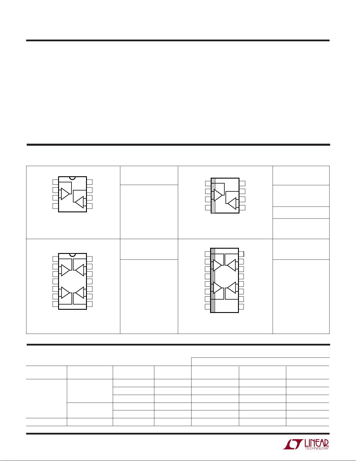
LT1215/LT1216
1
2
3
4
8
7
6
5
TOP VIEW
S8 PACKAGE
8-LEAD PLASTIC SO
B
A
OUT A
–IN A
+IN A
V
–
V
+
OUT B
–IN B
+IN B
TOP VIEW
S PACKAGE
16-LEAD PLASTIC SO
1
2
3
4
5
6
7
8
16
15
14
13
12
11
10
9
OUT A
–IN A
+IN A
V
+
+IN B
–IN B
OUT B
NC
OUT D
–IN D
+IN D
V
–
+IN C
–IN C
OUT C
NC
A
C
B
D
N PACKAGE
14-LEAD PDIP
OUT A
–IN A
+IN A
V
+
+IN B
–IN B
OUT B
OUT D
–IN D
+IN D
V
–
+IN C
–IN C
OUT C
1
2
3
4
5
6
7
14
13
12
11
10
9
8
D
A
C
B
TOP VIEW
A
W
O
LUTEXI TIS
S
A
WUW
U
ARB
G
Total Supply Voltage (V+ to V–) ............................. 36V
Input Current ..................................................... ±15mA
Output Short-Circuit Duration (Note 2)........ Continuous
Operating Temperature Range
LT1215C/LT1216C (Note 3) .............. –40°C to 85°C
LT1215M ......................................... –55°C to 125°C
Specified Temperature Range
LT1215C/LT1216C (Note 4) .............. –40°C to 85°C
LT1215M ......................................... –55°C to 125°C
WU
/
PACKAGE
OUT A
–IN A
+IN A
–
V
J8 PACKAGE
8-LEAD CERDIP
T
JMAX
T
JMAX
O
RDER I FOR ATIO
TOP VIEW
1
2
A
3
4
= 175°C, θJA = 100°C/W (J)
= 150°C, θJA = 100°C/W (N)
8
V
7
OUT B
6
–IN B
B
5
+IN B
N8 PACKAGE
8-LEAD PDIP
ORDER PART
+
NUMBER
LT1215CN8
LT1215ACN8
LT1215MJ8
LT1215AMJ8
(Note 1)
Storage Temperature Range ................ –65°C to 150°C
Junction Temperature (Note 5).............................150°C
Plastic Package (CN8, CS8, CN, CS)................ 150°C
Ceramic Package (MJ8) .................................. 175°C
Lead Temperature (Soldering, 10 sec)................. 300°C
U
ORDER PART
NUMBER
LT1215CS8
S8 PART MARKING
T
= 150°C, θJA = 150°C/W
JMAX
1215
ORDER PART
NUMBER
LT1216CS
T
= 150°C, θJA = 70°C/W
JMAX
ORDER PART
NUMBER
LT1216CN
T
= 150°C, θJA = 100°C/W
JMAX
U
AVAILABLE OPTIO S
NUMBER OF MAX TC V
OP AMPS T
Two (Dual) –40°C to 85°C 300µV2.5µV/°C LT1215ACN8
2
Four (Quad) –40°C to 85°C 450µV10µV/°C LT1216CN LT1216CS
RANGE MAX VOS (25°C) (∆VOS/∆T) (J) (N) (S)
A
450µV5µV/°C LT1215CN8
450µV10µV/°C LT1215CS8
–55°C to 125°C 300µV2.5µV/°C LT1215AMJ8
450µV5µV/°C LT1215MJ8
OS
CERAMIC PLASTIC DIP SURFACE MOUNT
PACKAGE
Page 3
LT1215/LT1216
LECTRICAL C CHARA TERIST
E
5V
VS = 5V, VCM = 0.5V, V
SYMBOL PARAMETER CONDITIONS MIN TYP MAX MIN TYP MAX UNITS
V
OS
∆V
∆Time
I
OS
I
B
e
n
i
n
CMRR Common Mode Rejection Ratio VCM = 0V to 3V 90 108 86 108 dB
PSRR Power Supply Rejection Ratio VS = 2.5V to 12.5V 96 115 93 115 dB
A
VOL
I
O
SR Slew Rate AV = –2 30 30 V/µs
GBW Gain-Bandwidth Product f = 100kHz 23 23 MHz
I
S
tr, t
OS Overshoot AV = 1, VO = 100mV 25 25 %
t
PD
t
S
THD Total Harmonic Distortion AV = 1, VO = 1V
Input Offset Voltage 125 300 150 450 µV
Long-Term Input Offset 0.8 1.0 µV/Mo
OS
Voltage Stability
Input Offset Current 35 80 35 120 nA
Input Bias Current 420 500 420 600 nA
Input Noise Voltage 0.1Hz to 10Hz 400 400 nV
Input Noise Voltage Density fO = 10Hz 15.0 15.0 nV/√Hz
Input Noise Current Density fO = 10Hz 7.0 7.0 pA/√Hz
Input Resistance (Note 6) Differential Mode 10 40 10 40 MΩ
Input Capacitance f = 1MHz 10 10 pF
Input Voltage Range 3.0 3.2 3.0 3.2 V
Large-Signal Voltage Gain VO = 0.05V to 3.7V, RL = 500Ω 150 600 150 600 V/mV
Maximum Output Voltage Swing Output High, No Load 4.30 4.39 4.30 4.39 V
(Note 7) Output High, I
Maximum Output Current (Note 11) ±30 ±50 ±30 ±50 mA
Supply Current Per Amplifier 3.6 4.75 6.6 3.6 4.75 6.6 mA
Minimum Supply Voltage Single Supply 2.2 2.5 2.2 2.5 V
Full Power Bandwidth AV = 1, VO = 2.5V
Rise Time, Fall Time AV = 1, 10% to 90%, VO = 100mV 16 16 ns
f
Propagation Delay AV = 1, VO = 100mV 13 13 ns
Settling Time 0.01%, AV = 1, ∆VO = 2V 250 250 ns
Open-Loop Output Resistance IO = 0mA, f = 10MHz 40 40 Ω
= 0.5V, TA = 25°C, unless otherwise noted.
OUT
fO = 1000Hz 12.5 12.5 nV/√Hz
fO = 1000Hz 0.5 0.5 pA/√Hz
Common Mode 200 200 MΩ
Output High, I
Output Low, No Load 0.005 0.008 0.005 0.008 V
Output Low, I
Output Low, I
ICS
LT1215AC LT1215C/LT1215M
LT1215AM LT1216C
0 – 0.2 0 – 0.2 V
= 1mA 4.20 4.30 4.20 4.30 V
SOURCE
= 30mA 3.60 3.75 3.60 3.75 V
SOURCE
= 1mA 0.030 0.050 0.030 0.050 V
SINK
= 30mA 0.630 1.000 0.630 1.000 V
SINK
P-P
, 20Hz to 20kHz 0.001 0.001 %
RMS
2.6 2.6 MHz
P-P
3
Page 4
LT1215/LT1216
LECTRICAL C CHARA TERIST
E
5V
VS = 5V, VCM = 0.5V, V
SYMBOL PARAMETER CONDITIONS MIN TYP MAX MIN TYP MAX UNITS
V
OS
∆V
∆T
I
OS
I
B
CMRR Common Mode Rejection Ratio VCM = 0.1V to 2.9V 89 108 85 108 dB
PSRR Power Supply Rejection Ratio VS = 2.6V to 12.5V 95 114 92 114 dB
A
VOL
I
S
Input Offset Voltage 200 350 250 550 µV
Input Offset Voltage Drift 8-Pin DIP Package 1 2.5 2 5 µV/°C
OS
(Note 6) 14-Pin DIP, SO Package 3 10 µV/°C
Input Offset Current 35 100 35 170 nA
Input Bias Current 450 530 450 830 nA
Input Voltage Range 2.9 3.1 2.9 3.1 V
Large-Signal Voltage Gain VO = 0.05V to 3.7V, RL = 500Ω 100 600 100 600 V/mV
Maximum Output Voltage Swing Output High, No Load 4.20 4.33 4.20 4.33 V
(Note 7) Output High, I
Supply Current Per Amplifier 3.3 5.2 7.5 3.3 5.2 7.5 mA
= 0.5V, 0°C ≤ TA ≤ 70°C, unless otherwise noted.
OUT
Output High, I
Output Low, No Load 0.006 0.009 0.006 0.009 V
Output Low, I
Output Low, I
ICS
LT1215AC LT1215C/LT1216C
0.1 –0.1 0.1 –0.1 V
= 1mA 4.10 4.24 4.10 4.24 V
SOURCE
= 20mA 3.70 3.89 3.70 3.89 V
SOURCE
= 1mA 0.035 0.055 0.035 0.055 V
SINK
= 20mA 0.500 0.725 0.500 0.725 V
SINK
VS = 5V, VCM = 0.5V, V
SYMBOL PARAMETER CONDITIONS MIN TYP MAX MIN TYP MAX UNITS
V
OS
∆V
∆T
I
OS
I
B
CMRR Common Mode Rejection Ratio VCM = 0.2V to 2.8V 88 108 84 108 dB
PSRR Power Supply Rejection Ratio VS = 2.7V to 12.5V 94 114 91 114 dB
A
VOL
I
S
Input Offset Voltage 200 400 250 600 µV
Input Offset Voltage Drift 8-Pin DIP Package 1 2.5 2 5 µV/°C
OS
(Note 6) 14-Pin DIP, SO Package 3 10 µV/°C
Input Offset Current 35 110 35 190 nA
Input Bias Current 450 550 450 850 nA
Input Voltage Range 2.8 3.0 2.8 3.0 V
Large-Signal Voltage Gain VO = 0.05V to 3.7V, RL = 500Ω 100 600 100 600 V/mV
Maximum Output Voltage Swing Output High, No Load 4.10 4.30 4.10 4.30 V
(Note 7) Output High, I
Supply Current Per Amplifier 2.9 5.3 7.6 2.9 5.3 7.6 mA
= 0.5V, –40°C ≤ TA ≤ 85°C, unless otherwise noted. (Note 4)
OUT
0.2 0 0.2 0 V
= 1mA 4.00 4.16 4.00 4.16 V
Output High, I
Output Low, No Load 0.006 0.010 0.006 0.010 V
Output Low, I
Output Low, I
SOURCE
= 20mA 3.60 3.82 3.60 3.82 V
SOURCE
= 1mA 0.035 0.060 0.035 0.060 V
SINK
= 20mA 0.500 0.750 0.500 0.750 V
SINK
LT1215AC LT1215C/LT1216C
4
Page 5
LT1215/LT1216
LECTRICAL C CHARA TERIST
E
5V
VS = 5V, VCM = 0.5V, V
SYMBOL PARAMETER CONDITIONS MIN TYP MAX MIN TYP MAX UNITS
V
OS
∆V
∆T
I
OS
I
B
CMRR Common Mode Rejection Ratio VCM = 0.4V to 2.8V 87 108 82 108 dB
PSRR Power Supply Rejection Ratio VS = 2.7V to 12.5V 93 114 90 114 dB
A
VOL
I
S
Input Offset Voltage 250 450 350 750 µV
Input Offset Voltage Drift 1 2.5 2 5 µV/°C
OS
(Note 6)
Input Offset Current 35 150 35 200 nA
Input Bias Current 450 600 450 700 nA
Input Voltage Range 2.8 3.0 2.8 3.0 V
Large-Signal Voltage Gain VO = 0.05V to 3.7V, RL = 500Ω 50 100 50 100 V/mV
Maximum Output Voltage Swing Output High, No Load 4.00 4.20 4.00 4.20 V
(Note 7) Output High, I
Supply Current Per Amplifier 2.3 5.5 8.4 2.3 5.5 8.4 mA
= 0.5V, –55°C ≤ TA ≤ 125°C, unless otherwise noted.
OUT
Output High, I
Output Low, No Load 0.007 0.012 0.007 0.012 mV
Output Low, I
Output Low, I
ICS
LT1215AM LT1215M
0.4 0.2 0.4 0.2 V
= 1mA 3.90 4.10 3.90 4.10 V
SOURCE
= 20mA 3.50 3.80 3.50 3.80 V
SOURCE
= 1mA 0.040 0.070 0.040 0.070 mV
SINK
= 20mA 0.700 1.000 0.700 1.000 mV
SINK
+
15V
–
VS = ±15V, VCM = 0V, V
SYMBOL PARAMETER CONDITIONS MIN TYP MAX MIN TYP MAX UNITS
V
OS
I
OS
I
B
CMRR Common Mode Rejection Ratio VCM = –15V to 13V 90 108 86 108 dB
PSRR Power Supply Rejection Ratio VS = ±2V to ±18V 96 110 93 110 dB
A
VOL
I
O
SR Slew Rate AV = –2 (Note 8) 40 50 40 50 V/µs
GBW Gain-Bandwidth Product f = 100kHz 15 23 15 23 MHz
I
S
LECTRICAL C CHARA TERIST
E
= 0V, TA = 25°C, unless otherwise noted.
OUT
Input Offset Voltage 225 500 250 650 µV
Input Offset Current 30 80 30 110 nA
Input Bias Current 360 500 360 550 nA
Input Voltage Range 13.0 13.2 13.0 13.2 V
Large-Signal Voltage Gain VO = 0V to ±10V, RL = 2k 1000 3500 1000 3500 V/mV
Maximum Output Voltage Swing Output High, I
Output Low, I
Maximum Output Current (Note 11) ±30 ±50 ±30 ±50 mA
Supply Current Per Amplifier 3.6 5.7 8 3.6 5.7 8 mA
Channel Separation VO = ±10V, RL = 2k 128 140 128 140 dB
Minimum Supply Voltage Equal Split Supplies ±1.7 ±2 ±1.7 ±2V
Full-Power Bandwidth AV = 1, VO = 20V
Settling Time 0.01%, AV = 1, ∆VO = 10V 480 480 ns
SOURCE
SINK
P-P
ICS
LT1215AC LT1215C/LT1215M
LT1215AM LT1216C
–15.0 –15.2 –15.0 – 15.2 V
= 30mA 13.5 13.75 13.5 13.75 V
= 30mA –14 –14.4 –14 –14.4 V
750 750 kHz
5
Page 6
LT1215/LT1216
+
15V
–
VS = ±15V, VCM = 0V, V
SYMBOL PARAMETER CONDITIONS MIN TYP MAX MIN TYP MAX UNITS
V
OS
∆V
OS
∆T
I
OS
I
B
CMRR Common Mode Rejection Ratio VCM = –14.9V to 12.9V 89 108 85 108 dB
PSRR Power Supply Rejection Ratio VS = ±2.1V to ±18V 95 110 92 110 dB
A
VOL
I
S
LECTRICAL C CHARA TERIST
E
= 0V, 0°C ≤ TA ≤ 70°C, unless otherwise noted.
OUT
Input Offset Voltage 325 550 400 750 µV
Input Offset Voltage Drift 8-Pin DIP Package 1 2.5 2 5 µV/°C
(Note 6) 14-Pin DIP, SO Package 3 10 µV/°C
Input Offset Current 30 100 30 160 nA
Input Bias Current 360 530 360 800 nA
Input Voltage Range 12.9 13.1 12.9 13.1 V
Large-Signal Voltage Gain VO = 0V to ±10V, RL = 2k 800 3000 800 3000 V/mV
Maximum Output Voltage Swing Output High, I
Output Low, I
Supply Current Per Amplifier 3.3 6.3 9.2 3.3 6.3 9.2 mA
SOURCE
SINK
ICS
LT1215AC LT1215C/LT1216C
–14.9 –15.1 –14.9 –15.1 V
= 20mA 13.7 13.9 13.7 13.9 V
= 20mA –14.2 –14.5 –14.2 –14.5 V
VS = ±15V, VCM = 0V, V
SYMBOL PARAMETER CONDITIONS MIN TYP MAX MIN TYP MAX UNITS
V
OS
∆V
∆T
I
OS
I
B
CMRR Common Mode Rejection Ratio VCM = –14.8V to 12.8V 88 108 84 108 dB
PSRR Power Supply Rejection Ratio VS = ±2.2V to ±18V 94 110 91 110 dB
A
VOL
I
S
Input Offset Voltage 325 600 400 800 µV
Input Offset Voltage Drift 8-Pin DIP Package 1 2.5 2 5 µV/°C
OS
(Note 6) 14-Pin DIP, SO Package 3 10 µV/°C
Input Offset Current 30 110 30 180 nA
Input Bias Current 360 550 360 820 nA
Input Voltage Range 12.8 13.0 12.8 13.0 V
Large-Signal Voltage Gain VO = 0V to ±10V, RL = 2k 800 2500 800 2500 V/mV
Maximum Output Voltage Swing Output High, I
Supply Current Per Amplifier 2.9 6.5 9.5 2.9 6.5 9.5 mA
VS = ±15V, VCM = 0V, V
SYMBOL PARAMETER CONDITIONS MIN TYP MAX MIN TYP MAX UNITS
V
OS
∆V
∆T
I
OS
I
B
CMRR Common Mode Rejection Ratio VCM = –14.6V to 12.8V 87 108 82 108 dB
PSRR Power Supply Rejection Ratio VS = ±2.2V to ±15V 93 110 90 110 dB
A
VOL
I
S
Input Offset Voltage 350 650 500 950 µV
Input Offset Voltage Drift 1 2.5 2 5 µV/°C
OS
(Note 6)
Input Offset Current 30 150 30 200 nA
Input Bias Current 360 600 360 700 nA
Input Voltage Range 12.8 13.0 12.8 13.0 V
Large-Signal Voltage Gain VO = 0V to ±10V, RL = 2k 500 2000 500 2000 V/mV
Maximum Output Voltage Swing Output High, I
Supply Current Per Amplifier 2.3 7 10.3 2.3 7 10.3 mA
= 0V, –40°C ≤ TA ≤ 85°C, unless otherwise noted. (Note 4)
OUT
–14.8 –15.0 –14.8 –15.0 V
= 20mA 13.6 13.8 13.6 13.8 V
SOURCE
Output Low, I
= 0V, –55°C ≤ TA ≤ 125°C, unless otherwise noted.
OUT
Output Low, I
= 20mA –14.1 –14.5 –14.1 –14.5 V
SINK
–14.6 –14.8 –14.6 –14.8 V
= 20mA 13.4 13.8 13.4 13.8 V
SOURCE
= 20mA –14 –14.5 –14 –14.5 V
SINK
LT1215AC LT1215C/LT1216C
LT1215AM LT1215M
6
Page 7

LT1215/LT1216
LECTRICAL C CHARA TERIST
3.3V
VS = 3.3V, VCM = 0.5V, V
SYMBOL PARAMETER CONDITIONS MIN TYP MAX MIN TYP MAX UNITS
V
OS
I
O
E
= 0.5V, TA = 25°C, unless otherwise noted. (Note 8)
OUT
Input Offset Voltage 125 300 150 450 µV
Input Voltage Range (Note 10) 1.3 1.5 1.3 1.5 V
Maximum Output Voltage Swing Output High, No Load 2.60 2.69 2.60 2.69 V
Output High, I
Output High, I
Output Low, No Load 0.005 0.008 0.005 0.008 V
Output Low, I
Output Low, I
Maximum Output Current ±30 ±50 ±30 ±50 mA
SOURCE
SOURCE
SINK
SINK
ICS
LT1215AC LT1215C/LT1215M
LT1215AM LT1216C
0 – 0.2 0 – 0.2 V
= 1mA 2.50 2.60 2.50 2.60 V
= 30mA 1.90 2.05 1.90 2.05 V
= 1mA 0.035 0.050 0.035 0.050 V
= 30mA 0.700 1.000 0.700 1.000 V
VS = 3.3V, VCM = 0.5V, V
SYMBOL PARAMETER CONDITIONS MIN TYP MAX MIN TYP MAX UNITS
V
OS
Input Offset Voltage 200 350 250 550 µV
Input Voltage Range (Note 10) 1.2 1.4 1.2 1.4 V
Maximum Output Voltage Swing Output High, No Load 2.50 2.63 2.50 2.63 V
VS = 3.3V, VCM = 0.5V, V
SYMBOL PARAMETER CONDITIONS MIN TYP MAX MIN TYP MAX UNITS
V
OS
Input Offset Voltage 200 400 250 600 µV
Input Voltage Range (Note 10) 1.1 1.3 1.1 1.3 V
Maximum Output Voltage Swing Output High, No Load 2.40 2.50 2.40 2.50 V
VS = 3.3V, VCM = 0.5V, V
SYMBOL PARAMETER CONDITIONS MIN TYP MAX MIN TYP MAX UNITS
V
OS
Input Offset Voltage 250 450 350 750 µV
Input Voltage Range (Note 10) 1.1 1.3 1.1 1.3 V
Maximum Output Voltage Swing Output High, No Load 2.30 2.50 2.30 2.50 V
= 0.5V, 0°C ≤ TA ≤ 70°C, unless otherwise noted. (Note 9)
OUT
LT1215AC LT1215C/LT1216C
0.1 –0.1 0.1 –0.1 V
Output High, I
Output High, I
Output Low, No Load 0.006 0.009 0.006 0.009 V
Output Low, I
Output Low, I
= 0.5V, –40°C ≤ TA ≤ 85°C, unless otherwise noted. (Notes 4, 9)
OUT
Output High, I
Output High, I
Output Low, No Load 0.006 0.010 0.006 0.010 V
Output Low, I
Output Low, I
= 0.5V, –55°C ≤ TA ≤ 125°C, unless otherwise noted. (Note 9)
OUT
Output High, I
Output High, I
Output Low, No Load 0.007 0.012 0.007 0.012 V
Output Low, I
Output Low, I
= 1mA 2.40 2.54 2.40 2.54 V
SOURCE
= 20mA 2.00 2.19 2.00 2.19 V
SOURCE
= 1mA 0.035 0.055 0.035 0.055 V
SINK
= 20mA 0.500 0.725 0.500 0.725 V
SINK
LT1215AC LT1215C/LT1216C
0.2 0 0.2 0 V
= 1mA 2.30 2.46 2.30 2.46 V
SOURCE
= 20mA 1.90 2.12 1.90 2.12 V
SOURCE
= 1mA 0.035 0.060 0.035 0.060 V
SINK
= 20mA 0.500 0.750 0.500 0.750 V
SINK
LT1215AM LT1215M
0.4 0.2 0.4 0.2 V
= 1mA 2.20 2.40 2.20 2.40 V
SOURCE
= 20mA 1.80 2.10 1.80 2.10 V
SOURCE
= 1mA 0.040 0.070 0.040 0.070 V
SINK
= 20mA 0.700 1.000 0.700 1.000 V
SINK
7
Page 8

LT1215/LT1216
INPUT OFFSET VOLTAGE (µV)
–750
PERCENT OF UNITS (%)
30
25
20
15
10
5
0
–450 –150 150 450
750
1215/16 G06
LT1215 N8 PACKAGE
LT1215 J8 PACKAGE
VS = ±15V
LECTRICAL C CHARA TERIST
E
ICS
Note 1: Absolute Maximum Ratings are those values beyond which the life
of a device may be impaired.
Note 2: A heat sink may be required to keep the junction temperature
below absolute maximum when the output is shorted indefinitely.
Note 3: The LT1215C/LT1216C are guaranteed functional over the
operating temperature range of –40°C to 85°C. The LT1215M is
guaranteed functional over the operating temperature range of
–55°C to 125°C.
Note 4: The LT1215C/LT1216C are guaranteed to meet specified
performance from 0°C to 70°C. The LT1215C/LT1216C are designed,
characterized and expected to meet specified performance from –40°C to
85°C but are not tested or QA sampled at these temperatures. For
guaranteed I-grade parts consult the factory. The LT1215M is guaranteed
to meet specified performance from –55°C to 125°C.
Note 5: T
dissipation P
is calculated from the ambient temperature TA and power
J
according to the following formulas:
D
UW
LPER
F
O
R
ATYPICA
CCHARA TERIST
E
C
LT1215MJ8, LT1215AMJ8: T
LT1215CN8, LT1215ACN8: T
LT1215CS8: T
LT1216CN: T
LT1216CS: T
= TA + (PD • 100°C/W)
J
= TA + (PD • 100°C/W)
J
= TA + (PD • 150°C/W)
J
= TA + (PD • 70°C/W)
J
= TA + (PD • 100°C/W)
J
Note 6: This parameter is not 100% tested.
Note 7: Guaranteed by correlation to 3.3V and ±15V tests.
Note 8: Slew rate is measured between ±8.5V on an output swing of ±10V
on ±15V supplies.
Note 9: Most LT1215/LT1216 electrical characteristics change very little
with supply voltage. See the 5V tables for characteristics not listed in the
3.3V table.
Note 10: Guaranteed by correlation to 5V and ±15V tests.
Note 11: Guaranteed by correlation to 3.3V tests.
ICS
50
45
40
35
30
25
20
15
PERCENT OF UNITS (%)
10
5
0
–525
50
45
40
35
30
25
20
15
PERCENT OF UNITS (%)
10
5
0
–525
Distribution of Offset Voltage Drift
Distribution of Input Offset Voltage with Temperature Distribution of Input Offset Voltage
VS = 5V
–225
–375
INPUT OFFSET VOLTAGE (µV)
LT1215 N8 PACKAGE
LT1215 J8 PACKAGE
–75
50
VS = 5V
40
30
20
PERCENT OF UNITS (%)
10
75
225
375
1215/16 G04
525
0
OFFSET VOLTAGE DRIFT WITH TEMPERATURE (µV/°C)
–3
–4
–5
–2 0 2
LT1215 N8 PACKAGE
LT1215 J8 PACKAGE
1
–1
3
4
1215/16 G05
5
Distribution of Offset Voltage Drift Distribution of Input Offset
Distribution of Input Offset Voltage with Temperature Voltage
VS = 5V
–225
–375
INPUT OFFSET VOLTAGE (µV)
LT1215 S8 PACKAGE
LT1216 N PACKAGE
LT1216 S PACKAGE
–75
50
VS = 5V
40
30
20
PERCENT OF UNITS (%)
10
75
225
375
1215/16 G07
525
0
OFFSET VOLTAGE DRIFT WITH TEMPERATURE (µV/°C)
–10
–6
–8
–4 0 4
LT1215 S8 PACKAGE
LT1216 N PACKAGE
LT1216 S PACKAGE
2
–2
6
8
1215/16 G08
10
30
VS = ±15V
25
20
15
10
PERCENT OF UNITS (%)
5
0
–750
–450 –150 150 450
INPUT OFFSET VOLTAGE (µV)
LT1215 S8 PACKAGE
LT1216 N PACKAGE
LT1216 S PACKAGE
750
1215/16 G09
8
Page 9

LT1215/LT1216
TOTAL SUPPLY VOLTAGE (V)
1
GAIN-BANDWIDTH PRODUCT (MHz)
23
22
21
20
19
18
17
10 40
1215/16 G12
60
50
40
30
20
10
0
3
5
7
20 30
PHASE MARGIN (DEG)
TA = –55°C TA = 25°C
TA = 125°C
TA = 25°C, 125°C
TA = –55°C
UW
LPER
R
F
O
ATYPICA
Voltage Gain vs Frequency Frequency Phase Margin vs Supply Voltage
140
120
100
80
60
40
VOLTAGE GAIN (dB)
20
0
–20
1
10
100
10k
1k 100k 10M
FREQUENCY (Hz)
CL = 20pF
= 2k
R
L
VS = ±15V
VS = 5V
1M
100M
1215/16 G10
Slew Rate vs Temperature Slew Rate vs Supply Voltage Capacitive Load Handling
60
TA = 25°C
= –2
A
V
= 10k
R
50
L
40
30
SLEW RATE (V/µs)
20
10
–50
–25
25
05075
TEMPERATURE (°C)
VS = ±15V
VS = 5V
100 125
1215/16 G13
CCHARA TERIST
C
E
ICS
Voltage Gain, Phase vs Gain-Bandwidth Product,
1215/16 G11
28
1215/16 G14
100
80
60
PHASE SHIFT (DEG)
40
20
0
–20
–40
–60
32
80
VS = 5V
70
60
50
40
30
OVERSHOOT (%)
20
10
0
10
60
40
GAIN
20
VOLTAGE GAIN (dB)
0
CL = 20pF
= 2k
R
L
–20
100k
65
AV = –2
= 10k
R
L
55
45
35
25
SLEW RATE (V/µs)
15
5
412
0
PHASE
VS = ±15V
VS = 5V
VS = ±15V
VS = 5V
1M 10M 100M
FREQUENCY (Hz)
TA = 125°C
TA = 25°C
TA = –55°C
8
TOTAL SUPPLY VOLTAGE (V)
20 36
24
16
AV = 1
AV = 5
AV = 10
100 1000
CAPACITIVE LOAD (pF)
1216/ G15
Undistorted Output Swing Undistorted Output Swing Total Harmonic Distortion and
vs Frequency, VS = 5V vs Frequency, VS = ±15V Noise vs Frequency
5
AV = –1
4
)
P-P
3
2
OUTPUT SWING (V
1
0
1k
AV = 1
VS = 5V
10k 100k 1M
FREQUENCY (Hz)
1215/16 G16
30
28
26
)
24
P-P
22
20
18
16
OUTPUT SWING (V
14
12
VS = ±15V
10
1k
AV = –1
AV = 1
10k 100k 1M
FREQUENCY (Hz)
1215/16 G17
0.1
VS = 5V
V
= 3V
O
P-P
RL = 1k
0.01
AV = 10
0.001
0.0001
TOTAL HARMONIC DISTORTION AND NOISE (%)
10 1k 10k 100k
AV = 1
100
FREQUENCY (Hz)
1215/16 G18
9
Page 10

LT1215/LT1216
UW
LPER
R
F
O
ATYPICA
Open-Loop Voltage Gain Positive Output Saturation
vs Supply Voltage Open-Loop Gain, VS = 5V Voltage vs Temperature
7k
RL = 2k
6k
5k
4k
3k
2k
1k
OPEN-LOOP VOLTAGE GAIN (V/mV)
0
412
8
0
TOTAL SUPPLY VOLTAGE (V)
16
TA = –55°C
TA = 25°C
TA = 125°C
28
20 36
32
24
1215/16 G19
Voltage Gain vs Load Resistance Open-Loop Gain, VS = ±15V Voltage vs Temperature
10k
TA = 25°C
1k
100
VS = 5V
VS = ±15V
CCHARA TERIST
E
C
RL = 2k
=
R
L
INPUT, 5µV/DIV
500Ω
01234
OUTPUT (V)
RL = 2k
R
INPUT, 5µV/DIV
L =
500Ω
ICS
1215/16 G20
1.6
= 5V
V
S
(V)
1.4
OUT
– V
+
1.2
1.0
0.8
0.6
SATURATION VOLTAGE, V
0.4
–50
I
SOURCE
–25 0
= 10µA
25 75
TEMPERATURE (°C)
Negative Output Saturation
1000
(mV)
–
– V
100
OUT
10
I
= 30mA
SOURCE
I
= 10mA
SOURCE
I
= 1mA
SOURCE
50 100 125
1215/16 G21
I
= 30mA
SINK
I
= 10mA
SINK
I
= 1mA
SINK
I
= 10µA
SINK
OPEN-LOOP VOLTAGE GAIN (V/mV)
10
10
100 1k 10k
LOAD RESISTANCE (Ω)
1215/16 G22
–10 0 10
OUTPUT (V)
1215/16 G23
SATURATION VOLTAGE, V
VS = 5V
1
–50
0 25 50 10075
–25 125
TEMPERATURE (°C)
Output Short-Circuit Current
Channel Separation vs Frequency vs Temperature Output Impedance vs Frequency
140
130
120
110
100
90
80
70
60
CHANNEL SEPARATION (dB)
50
40
30
10k 100k 10M
FREQUENCY (Hz)
1M
VS = ±15V
T
A
= 25°C
1215/16 G25
70
60
50
VS = ±15V
SINKING OR
40
OUTPUT SHORT-CIRCUIT CURRENT (mA)
30
–50
SOURCING
–25 0
CASE TEMPERATURE (°C)
VS = 5V
SOURCING
50 100 125
25 75
1215/16 G26
1000
OUTPUT IMPEDANCE (Ω)
0.01
100
0.1
10
1
10k
VS = ±15V
AV = 100
AV = 10 AV = 1
100k 1M 10M
FREQUENCY (Hz)
1215/16 G24
1215/16 G27
10
Page 11

LPER
LT1215/LT1216
UW
R
F
O
ATYPICA
CCHARA TERIST
E
C
ICS
5V Small-Signal Response
20mV/DIV
V
= 5V
S
= 1 1215/16 G34
A
V
50ns/DIV
±15V Small-Signal Response
20mV/DIV
5V Large-Signal Response
3V
0V
V
= 5V
S
= 1 1215/16 G28
A
V
200ns/DIV
±15V Large-Signal Response
10V
0V
–10V
5V Large-Signal Response
3V
0V
V
= 5V
S
= –1
A
V
= RG = 1k
R
F
C
= 20pF 1215/16 G31
F
100ns/DIV
±15V Large-Signal Response
10V
0V
–10V
= ±15V
V
S
= 1 1215/16 G34
A
V
50ns/DIV
5V Settling
500mV/DIV
= 5V
V
S
A
= 1 1215/16 G30
V
50ns/DIV
250µV/DIV
= ±15V
V
S
= 1 1215/16 G29
A
V
200ns/DIV
±15V Settling
2V/DIV
= ±15V
V
S
= –1 1215/16 G33
A
V
100ns/DIV
1mV/DIV
= ±15V
V
S
A
= –1
V
= RG = 1k 1215/16 G32
R
F
200ns/DIV
Settling Time to 0.01%
vs Output Step
10
VS = ±15V
8
6
4
2
0
–2
OUTPUT STEP (V)
–4
–6
–8
–10
200
NONINVERTING
300
SETTLING TIME (ns)
INVERTING
400
500
1215/16 G36
11
Page 12

LT1215/LT1216
TIME AFTER POWER-UP (SEC)
0
CHANGE IN OFFSET VOLTAGE (
µ
V)
20
15
10
5
0
–5
–10
–15
–20
160
1215/16 G03
40
80
120
200
180
140
100
6020
VS = ±2.5V
R
L
=
∞
4 TYPICAL AMPLIFIERS
FREQUENCY (Hz)
120
110
100
90
80
70
60
50
40
30
20
1k 100k 1M 10M
1215/16 G42
10k
NEGATIVE SUPPLY
POWER SUPPLY REJECTION RATIO (dB)
VS = ±15V
A
V
= 100
POSITIVE SUPPLY
UW
LPER
R
F
O
ATYPICA
Supply Current vs Supply Votage Supply Current vs Temperature Warm-Up Drift vs Time
6.5
6.0
5.5
5.0
4.5
4.0
3.5
3.0
2.5
SUPPLY CURRENT PER AMPLIFIER (mA)
2.0
0
2
13
SUPPLY VOLTAGE (V)
TA = 125°C
TA = 25°C
TA = –55°C
4
1215/16 G01
Input Bias Current vs Temperature Common Mode Voltage vs Temperature
400
380
360
340
320
300
280
INPUT BIAS CURRENT (nA)
260
240
–50
I
OS
–25 0
TEMPERATURE (°C)
+I
B
–I
B
50 100 125
25 75
VS = 5V
1215/16 G37
CCHARA TERIST
E
C
8
7
6
VS = ±15V
5
4
3
SUPPLY CURRENT PER AMPLIFIER (mA)
2
–50
5
–25
Input Bias Current vs Common Mode Range
0
VS = 5V
–100
–200
–300
INPUT BIAS CURRENT (nA)
–400
–500
TA = 25°C
0
–1
COMMON-MODE VOLTAGE (V)
ICS
VS = 5V
25
05075
TEMPERATURE (°C)
TA = 125°C
TA = –55°C
1
100 125
1215/16 G02
2
3
1215/16 G38
+
V
V+–1
+
V
–2
V–+1
–
V
COMMON-MODE RANGE (V)
V––1
4
–50 25 75
–25 0
TEMPERATURE (°C)
50 100 125
1215/16 G39
Input Noise Current, Noise Common Mode Rejection Ratio Input Referred Power Supply
Voltage Density vs Frequency vs Frequency Rejection Ratio vs Frequency
20
VS = ±15V
18
= 25°C
T
A
= 0Ω
R
S
16
14
12
10
8
6
4
2
INPUT NOISE VOLTAGE DENSITY (nV/√Hz)
INPUT NOISE CURRENT DENSITY (pA/√Hz)
0
10 1k 10k 100k
12
100
FREQUENCY (Hz)
VOLTAGE NOISE
CURRENT NOISE
1215/16 G40
110
VS = 5V
100
90
80
70
60
50
40
30
20
COMMON-MODE REJECTION RATIO (dB)
10
10k
100k 1M 10M
FREQUENCY (Hz)
1215/16 G41
Page 13

LT1215/LT1216
U
O
PPLICATI
A
Supply Voltage
The LT1215/LT1216 op amps are fully functional and all
internal bias circuits are in regulation with 2.2V of supply.
The amplifiers will continue to function with as little as
1.5V, although the input common mode range and the
phase margin are about gone. The minimum operating
supply voltage is guaranteed by the PSRR tests which are
done with the input common mode equal to 500mV and a
minimum supply voltage of 2.5V. The LT1215/LT1216 are
guaranteed over the full –55°C to 125°C range with a
minimum supply voltage of 2.7V.
The positive supply pin of the LT1215/LT1216 should be
bypassed with a small capacitor (about 0.01µF) within an
inch of the pin. When driving heavy loads and for good
settling time, an additional 4.7µF capacitor should be
used. When using split supplies, the same is true for the
negative supply pin.
S
I FOR ATIO
WU
U
For example, calculate the worst case power dissipation
while operating on ±15V supplies and driving a 500Ω load.
I
= 8.4 + 0.076 • (30 – 5) = 10.3mA
SMAX
P
= 2 • VS • I
DMAX
P
= 2 • 15V • 10.3mA + (15V – 7.5V) • 7.5V/500
DMAX
= 0.309 + 0.113 = 0.422 Watt per Amp
If this is the dual LT1215, the total power in the package is
twice that, or 0.844W. Now calculate how much the die
temperature will rise above the ambient. The total power
dissipation times the thermal resistance of the package
gives the amount of temperature rise. For this example, in
the SO-8 surface mount package, the thermal resistance is
150°C/W junction-to-ambient in still air.
Temperature Rise = P
= 126.6°C
SMAX
+ (VS – V
• θJA = 0.844W • 150°C/W
DMAX
OMAX
) • V
OMAX/RL
Power Dissipation
The LT1215/LT1216 amplifiers combine high speed and
large output current drive into very small packages. Because these amplifiers work over a very wide supply range,
it is possible to exceed the maximum junction temperature
under certain conditions. To insure that the LT1215/
LT1216 are used properly, calculate the worst case power
dissipation, define the maximum ambient temperature,
select the appropriate package and then calculate the
maximum junction temperature.
The worst case amplifier power dissipation is the total of
the quiescent current times the total power supply voltage
plus the power in the IC due to the load. The quiescent
supply current of the LT1215/LT1216 has a positive temperature coefficient. The maximum supply current of each
amplifier at 125°C is given by the following formula:
I
= 8.4 + 0.076 • (VS – 5) in mA
SMAX
VS is the total supply voltage.
The power in the IC due to the load is a function of the
output voltage, the supply voltage and load resistance. The
worst case occurs when the output voltage is at half
supply, if it can go that far, or its maximum value if it
cannot reach half supply.
The maximum junction temperature allowed in the plastic
package is 150°C. Therefore the maximum ambient allowed is the maximum junction temperature less the
temperature rise.
Maximum Ambient = 150°C – 126.6°C = 23.4°C
That means the SO-8 dual can only be operated at or below
room temperature on ±15V supplies with a 500Ω load.
Obviously this is not recommended. Lowering the supply
voltage is recommended, or use the DIP packaged part.
As a guideline to help in the selection of the LT1215/
LT1216, the following table describes the maximum supply voltage that can be used with each part based on the
following assumptions:
1. The maximum ambient is 70°C or 125°C depending
on the part rating.
2. The load is 500Ω, includes the feedback resistors.
3. The output can be anywhere between the supplies.
PART MAX SUPPLIES MAX POWER AT MAX T
LT1215MJ8 15.0V or ±10.3V 500mW
LT1215CN8 20.3V or ±14.5V 800mW
LT1215CS8 15.7V or ±10.8V 533mW
LT1216CN 16.4V or ±11.4V 1143mW
LT1216CS 13.0V or ±8.7V 800mW
A
13
Page 14

LT1215/LT1216
U
O
PPLICATI
A
Inputs
Typically at room temperature, the inputs of the LT1215/
LT1216 can common mode 400mV below ground (V–)
and to within 1.5V of the positive supply with the amplifier
still functional. However the input bias current and offset
voltage will shift as shown in the characteristic curves. For
full precision performance, the common mode range
should be limited between ground (V–) and 2V below the
positive supply.
When either of the inputs is taken below ground (V–) by
more than about 700mV, that input current will increase
dramatically. The current is limited by internal 100Ω
resistors between the input pins and diodes to each
supply. The output will remain low (no phase reversal) for
inputs 1.3V below ground (V–). If the output does not have
to sink current, such as in a single supply system with a 1k
load to ground, there is no phase reversal for inputs up to
8V below ground.
There are no clamps across the inputs of the LT1215/
LT1216 and therefore each input can be forced to any
voltage between the supplies. The input current will remain constant at about 360nA over most of this range.
When an input gets closer than 2V to the positive supply,
that input current will gradually decrease to zero until the
input goes above the supply, then it will increase due to the
previously mentioned diodes. If the inverting input is held
more positive than the noninverting input by 200mV or
more, while at the same time the noninverting input is
within 300mV of ground (V–), then the supply current will
increase by 5mA and the noninverting input current will
increase to about 100µA. This should be kept in mind in
comparator applications where the inverting input stays
above ground (V–) and the noninverting input does not.
Output
The output of the LT1215/LT1216 will swing to within
0.61V of the positive supply with no load. The open-loop
output resistance, when the output is driven hard into the
positive rail, is about 100Ω as the output starts to source
S
I FOR ATIO
WU
U
current; this resistance drops to about 20Ω as the current
increases. Therefore when the output sources 1mA, the
output will swing to within 0.7V of the positive supply.
While sourcing 30mA, it is within 1.25V of the positive
supply.
The output of the LT1215/LT1216 will swing to within 5mV
of the negative supply while sinking zero current. Thus, in
a typical single supply application with the load going to
ground, the output will go to within 5mV of ground. The
open-loop output resistance when the output is driven
hard into the negative rail is about 25Ω at low currents and
reduces to about 21Ω at high currents. Therefore when the
output sinks 1mA, the output is about 30mV above the
negative supply and while sinking 30mA, it is about
630mV above it.
The output of the LT1215/LT1216 has reverse-biased
diodes to each supply. If the output is forced beyond either
supply, unlimited currents will flow. If the current is
transient and limited to several hundred mA, no damage
will occur.
Feedback Components
Because the input currents of the LT1215/LT1216 are less
than 600nA, it is possible to use high value feedback
resistors to set the gain. However, care must be taken to
insure that the pole that is formed by the feedback resistors and the input capacitance does not degrade the
stability of the amplifier. For example, if a single supply,
noninverting gain of two is set with two 10k resistors, the
LT1215/LT1216 will probably oscillate. This is because
the amplifier goes open-loop at 7MHz (6dB of gain) and
has 50° of phase margin. The feedback resistors and the
10pF input capacitance generate a pole at 3MHz that
introduces 67° of phase shift at 7MHz! The solution is
simple, lower the values of the resistors or add a feedback
capacitor of 10pF or more.
14
Page 15

LT1215/LT1216
PPLICATI
A
U
O
S
I FOR ATIO
WU
U
Comparator Applications
Sometimes it is desirable to use an op amp as a comparator. When operating the LT1215/LT1216 on a single 3.3V
or 5V supply, the output interfaces directly with most TTL
and CMOS logic.
The response time of the LT1215/LT1216 is a strong
function of the amount of input overdrive as shown in the
LT1215 Comparator Response (+)
20mV, 10mV, 5mV, 2mV Overdrives
4
2
OUTPUT (V)
0
following photos. These amplifiers are unity-gain stable
op amps and not fast comparators, therefore, the logic
being driven may oscillate due to the long transition time.
The output can be speeded up by adding 20mV or more of
hysteresis (positive feedback), but the offset is then a
function of the input direction.
LT1215 Comparator Response (–)
20mV, 10mV, 5mV, 2mV Overdrives
4
2
OUTPUT (V)
0
100
0
INPUT (mV)
= 5V 1215/16 AI01
V
S
R
= ∞
L
W
SPL
I
IIFED S
Q7
Q9
100
0
INPUT (mV)
5µs/DIV
= 5V 1215/16 AI02
V
S
R
= ∞
L
5µs/DIV
W
A
E
CH
I
1
–IN
Q8
I
Q1
C
I
C
TI
+
V
Q12
I
6
BIAS
Q13
Q14
Q15
OUT
Q16
C
I
O
8
–
V
1215/16 SS
I
3
2
Q4
Q3
Q5
Q6
I
4
+IN
Q2
Q10
I
5
C
M
Q11
R
F
C
F
I
7
15
Page 16

LT1215/LT1216
TYPICAL APPLICATIO
Single Supply, AC Coupled Input, RMS Calibrated, Average Detector
U
AC TO DC BIASED
DIFFERENTIAL SIGNAL
20k
10k
+
LT1216
5V
V
A
B
–
11.3k
22pF
+
10µF
+
V
IN
1k
LT1216
–
D
11.3k
22pF
V
A
DIFFERENTIAL INPUT,
ABSOLUTE VALUE CIRCUIT
R1
10k
R1
10k
R1
10k
R1
10k
2 × R2
20k
–
LT1216
+
+
LT1216
–
22pF
2 × R2
20k
B
R2
10k
C
R2
10k
22pF
DC OUTPUT VOLTAGE vs AC INPUT VOLTAGE
1000
VS = 5V
100
DC OUT (mV)
R2
•
– V
V
A
R1
100k
B
f = 1kHz
f = 100kHz
10
1
+
1µF
10 100
AC IN (mV
DC OUT
1215/16 TA05
RMS
)
1215/16 GA06
16
Page 17

PACKAGE DESCRIPTIO
LT1215/LT1216
U
Dimensions in inches (millimeters) unless otherwise noted.
J8 Package
8-Lead CERDIP (Narrow 0.300, Hermetic)
(LTC DWG # 05-08-1110)
CORNER LEADS OPTION
(4 PLCS)
0.023 – 0.045
(0.584 – 1.143)
HALF LEAD
0.045 – 0.068
(1.143 – 1.727)
FULL LEAD
OPTION
0.300 BSC
(0.762 BSC)
0.008 – 0.018
(0.203 – 0.457)
NOTE: LEAD DIMENSIONS APPLY TO SOLDER DIP/PLATE
OR TIN PLATE LEADS
0° – 15°
OPTION
0.005
(0.127)
MIN
0.025
(0.635)
RAD TYP
0.045 – 0.065
(1.143 – 1.651)
0.014 – 0.026
(0.360 – 0.660)
0.405
(10.287)
MAX
87
12
65
3
4
0.220 – 0.310
(5.588 – 7.874)
0.015 – 0.060
(0.381 – 1.524)
0.100
(2.54)
BSC
0.200
(5.080)
MAX
0.125
3.175
MIN
J8 1298
17
Page 18

LT1215/LT1216
PACKAGE DESCRIPTIO
U
Dimensions in inches (millimeters) unless otherwise noted.
N8 Package
8-Lead PDIP (Narrow 0.300)
(LTC DWG # 05-08-1510)
0.400*
(10.160)
MAX
876
0.255 ± 0.015*
(6.477 ± 0.381)
5
12
0.300 – 0.325
(7.620 – 8.255)
0.065
(1.651)
0.009 – 0.015
(0.229 – 0.381)
+0.035
0.325
–0.015
+0.889
8.255
()
–0.381
*THESE DIMENSIONS DO NOT INCLUDE MOLD FLASH OR PROTRUSIONS.
MOLD FLASH OR PROTRUSIONS SHALL NOT EXCEED 0.010 INCH (0.254mm)
TYP
0.045 – 0.065
(1.143 – 1.651)
0.100
(2.54)
BSC
N Package
14-Lead PDIP (Narrow 0.300)
(LTC DWG # 05-08-1510)
14
0.255 ± 0.015*
(6.477 ± 0.381)
1213
3
0.770*
(19.558)
MAX
11
4
0.130 ± 0.005
(3.302 ± 0.127)
0.125
(3.175)
MIN
0.018 ± 0.003
(0.457 ± 0.076)
8910
0.020
(0.508)
MIN
N8 1098
18
2
0.300 – 0.325
(7.620 – 8.255)
0.009 – 0.015
(0.229 – 0.381)
+0.035
0.325
–0.015
+0.889
8.255
()
–0.381
*THESE DIMENSIONS DO NOT INCLUDE MOLD FLASH OR PROTRUSIONS.
MOLD FLASH OR PROTRUSIONS SHALL NOT EXCEED 0.010 INCH (0.254mm)
0.020
(0.508)
MIN
0.130 ± 0.005
(3.302 ± 0.127)
0.125
(3.175)
MIN
0.005
(0.125)
MIN
31
0.045 – 0.065
(1.143 – 1.651)
0.100
(2.54)
BSC
6
7
0.065
(1.651)
TYP
0.018 ± 0.003
(0.457 ± 0.076)
N14 1098
5
4
Page 19

PACKAGE DESCRIPTIO
U
Dimensions in inches (millimeters) unless otherwise noted.
S8 Package
8-Lead Plastic Small Outline (Narrow 0.150)
(LTC DWG # 05-08-1610)
0.189 – 0.197*
(4.801 – 5.004)
7
8
5
6
LT1215/LT1216
0.228 – 0.244
(5.791 – 6.197)
0.010 – 0.020
(0.254 – 0.508)
0.008 – 0.010
(0.203 – 0.254)
*
DIMENSION DOES NOT INCLUDE MOLD FLASH. MOLD FLASH
SHALL NOT EXCEED 0.006" (0.152mm) PER SIDE
**
DIMENSION DOES NOT INCLUDE INTERLEAD FLASH. INTERLEAD
FLASH SHALL NOT EXCEED 0.010" (0.254mm) PER SIDE
×
°
45
0.016 – 0.050
(0.406 – 1.270)
0°– 8° TYP
S Package
16-Lead Plastic Small Outline (Narrow 0.150)
(LTC DWG # 05-08-1610)
0.053 – 0.069
(1.346 – 1.752)
0.014 – 0.019
(0.355 – 0.483)
TYP
16
15
1
2
0.386 – 0.394*
(9.804 – 10.008)
13
14
0.150 – 0.157**
(3.810 – 3.988)
3
4
0.004 – 0.010
(0.101 – 0.254)
0.050
(1.270)
BSC
SO8 1298
12
11
10
9
0.010 – 0.020
(0.254 – 0.508)
0.008 – 0.010
(0.203 – 0.254)
*
DIMENSION DOES NOT INCLUDE MOLD FLASH. MOLD FLASH
SHALL NOT EXCEED 0.006" (0.152mm) PER SIDE
**
DIMENSION DOES NOT INCLUDE INTERLEAD FLASH. INTERLEAD
FLASH SHALL NOT EXCEED 0.010" (0.254mm) PER SIDE
× 45°
0° – 8° TYP
0.016 – 0.050
(0.406 – 1.270)
Information furnished by Linear Technology Corporation is believed to be accurate and reliable.
However, no responsibility is assumed for its use. Linear Technology Corporation makes no representation that the interconnection of its circuits as described herein will not infringe on existing patent rights.
0.228 – 0.244
(5.791 – 6.197)
0.053 – 0.069
(1.346 – 1.752)
0.014 – 0.019
(0.355 – 0.483)
TYP
0.150 – 0.157**
(3.810 – 3.988)
4
5
0.050
(1.270)
BSC
3
2
1
7
6
8
0.004 – 0.010
(0.101 – 0.254)
S16 1098
19
Page 20

LT1215/LT1216
TYPICAL APPLICATIO
U
LT1216 Photo Diode Amplifier
TRANSIENT RESPONSE
5V
2V
+
–
I TO V BANDWIDTH = 7MHz
1/4
LT1216
5.1k
8pF
V
1215/16 TA03
OUT
1215/16 TA05
RELATED PARTS
PART NUMBER DESCRIPTION COMMENTS
LT1211/LT1212 Dual/Quad 14MHz, 7V/µs Single Supply Precision Op Amps Input Common Mode Includes Ground, 275µV VOS (Max),
6µV/°C Max Drift, 1.8mA Max Supply Current per Amplifier
LT1213/LT1214 Dual/Quad 28MHz, 12V/µs Single Supply Precision Op Amps Input Common Mode Includes Ground, 275µV VOS (Max),
6µV/°C Max Drift, 3.5mA Max Supply Current per Amplifier
LT1498/LT1499 10MHz, 6V/µs, Dual/Quad Rail-to-Rail Input and 475µV VOS (Max), 2.2mA Max Supply Current per Amplifier,
Output Precision C-Load
LT1124/LT1125 12.5MHz, 4.5V/µs, Dual/Quad Low Noise, 70µV VOS (Max), 2.75mA Max Supply Current per Amplifier,
High Speed Precision Op Amps 1µV/°C Max Drift
LT1355/LT1356 Dual and Quad 12MHz, 400V/µs Op Amps 1.25mA Max Supply Current per Amplifier, 800µV VOS (Max),
LT1358/LT1359 Dual and Quad 25MHz, 600V/µs Op Amps 2.5mA Max Supply Current per Amplifier, 600µV VOS (Max),
LT1361/LT1362 Dual and Quad 50MHz, 800V/µs Op Amps 5mA Max Supply Current per Amplifier, 1mV VOS (Max),
C-Load is a trademark of Linear Technology Corporation.
Linear Technology Corporation
20
1630 McCarthy Blvd., Milpitas, CA 95035-7417
(408) 432-1900 ● FAX: (408) 434-0507
TM
Op Amps 2.5µV/°C Max Drift, Stable with Capacitive Loads to 10,000pF
Drives All Capacitive Loads
Drives All Capacitive Loads
Drives All Capacitive Loads
sn12156, 12156fas LT/TP 1299 2K REV A • PRINTED IN USA
●
www.linear-tech.com
LINEAR TECHNOLOGY CORPORATION 1993
 Loading...