

Page 1
LT1204
4-Input Video Multiplexer
with 75MHz Current
Feedback Amplifier
EATU
F
■
0.1dB Gain Flatness > 30MHz
■
Channel Separation at 10MHz: 90dB
■
40mV Switching Transient, Input Referred
■
–3dB Bandwidth, AV = 2, RL = 150Ω: 75MHz
■
Channel-to-Channel Switching Time: 120ns
■
Easy to Expand for More Inputs
■
Large Input Range: ±6V
■
0.04% Differential Gain, RL = 150Ω
■
0.06° Differential Phase, RL = 150Ω
■
High Slew Rate: 1000V/µs
■
Output Swing, RL = 400Ω: ±13V
■
Wide Supply Range: ±5V to ±15V
PPLICATI
A
■
Broadcast Quality Video Multiplexing
■
Large Matrix Routing
■
Medical Imaging
■
Large Amplitude Signal Multiplexing
■
Programmable Gain Amplifiers
RE
S
O
U
S
DUESCRIPTIO
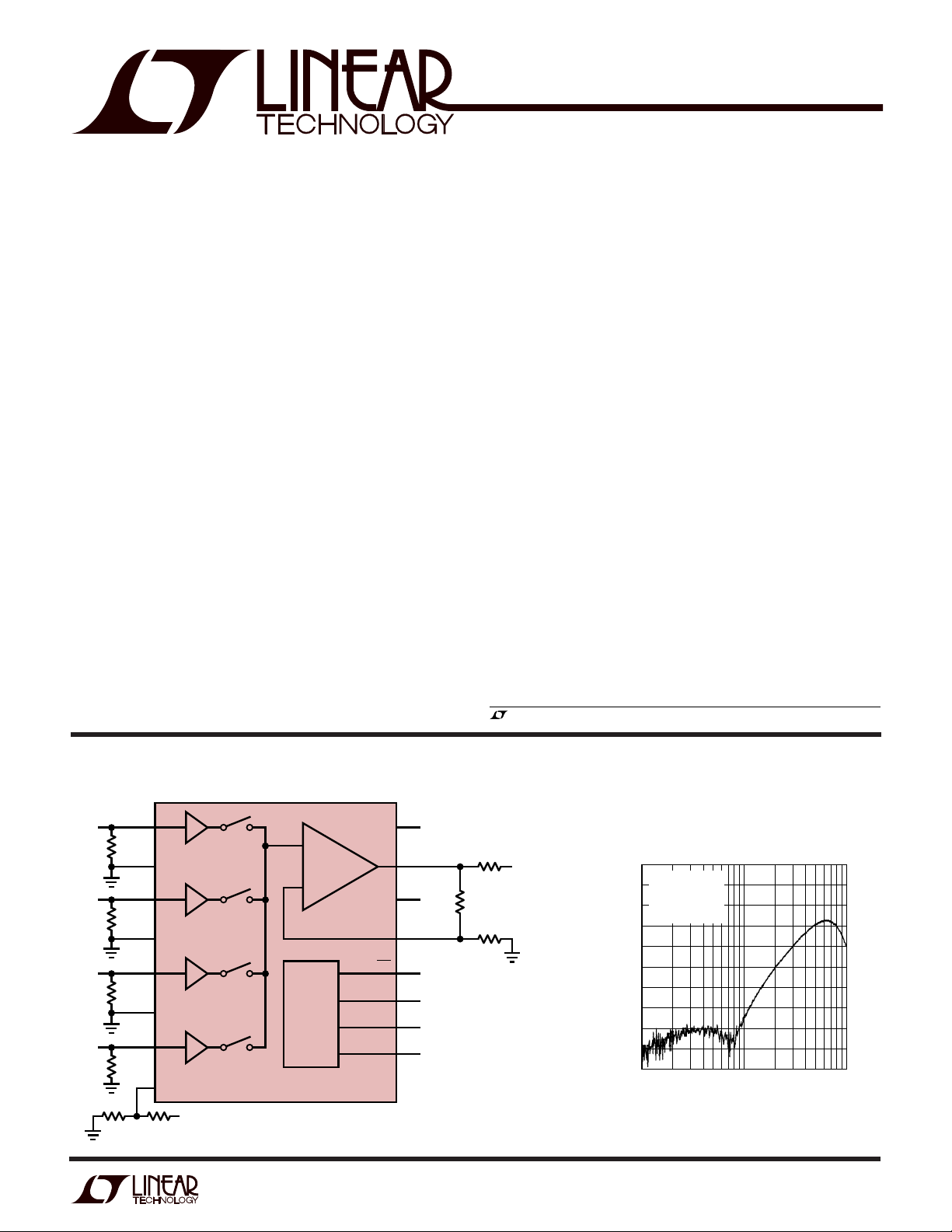
The LT®1204 is a 4-input video multiplexer designed to
drive 75Ω cables and easily expand into larger routing
systems. Wide bandwidth, high slew rate, and low differential gain and phase make the LT1204 ideal for broadcast
quality signal routing. Channel separation and disable
isolation are greater than 90dB up to 10MHz. The channelto-channel output switching transient is only 40mV
with a 50ns duration, making the transition imperceptible
on high quality monitors.
A unique feature of the LT1204 is its ability to expand into
larger routing matrices. This is accomplished by a patent
pending circuit that bootstraps the feedback resistors in
the disable condition, raising the true output impedance of
the circuit. The effect of this feature is to eliminate cable
misterminations in large systems.
The large input and output signal levels supported by the
LT1204 when operated on ±15V supplies make it ideal for
general purpose analog signal selection and multiplexing.
A shutdown feature reduces the supply current to 1.5mA.
P-P
,
, LTC and LT are registered trademarks of Linear Technology Corporation.
U
O
A
PPLICATITYPICAL
V
1
2
3
4
5
6
7
8
8.2k
IN0
GND
V
IN1
GND
V
IN2
GND
V
IN3
REF
+1
+1
+1
+1
–15V
+
CFA
–
LOGIC
LT1204
V
IN0
75Ω
V
IN1
75Ω
V
IN2
75Ω
V
IN3
75Ω
6.8k
S/D
ENABLE
16
+
15V
V
V
15
O
14
–
V
–15V
FB
13
12
11
A1
10
9
A0
1204 TA01
75Ω
V
OUT
R
F
1k
R
G
1k
–20
–40
–60
–80
–100
ALL HOSTILE CROSSTALK (dB)
–120
All Hostile Crosstalk
Surface Mount PCB Measurements
VS = ±15V
V
= GND
IN 0
= 0dBm
V
IN 1,2,3
= 100Ω
R
L
1
10 100
FREQUENCY (MHz)
1204 TA02
1
Page 2
LT1204
A
W
O
LUTEXI TIS
S
A
WUW
U
ARB
G
Supply Voltage ..................................................... ±18V
– Input Current (Pin 13) .................................... ±15mA
+Input and Control/Logic Current (Note 1) ........ ±50mA
Output Short-Circuit Duration (Note 2).........Continuous
Specified Temperature Range (Note 3)....... 0°C to 70°C
WU
/
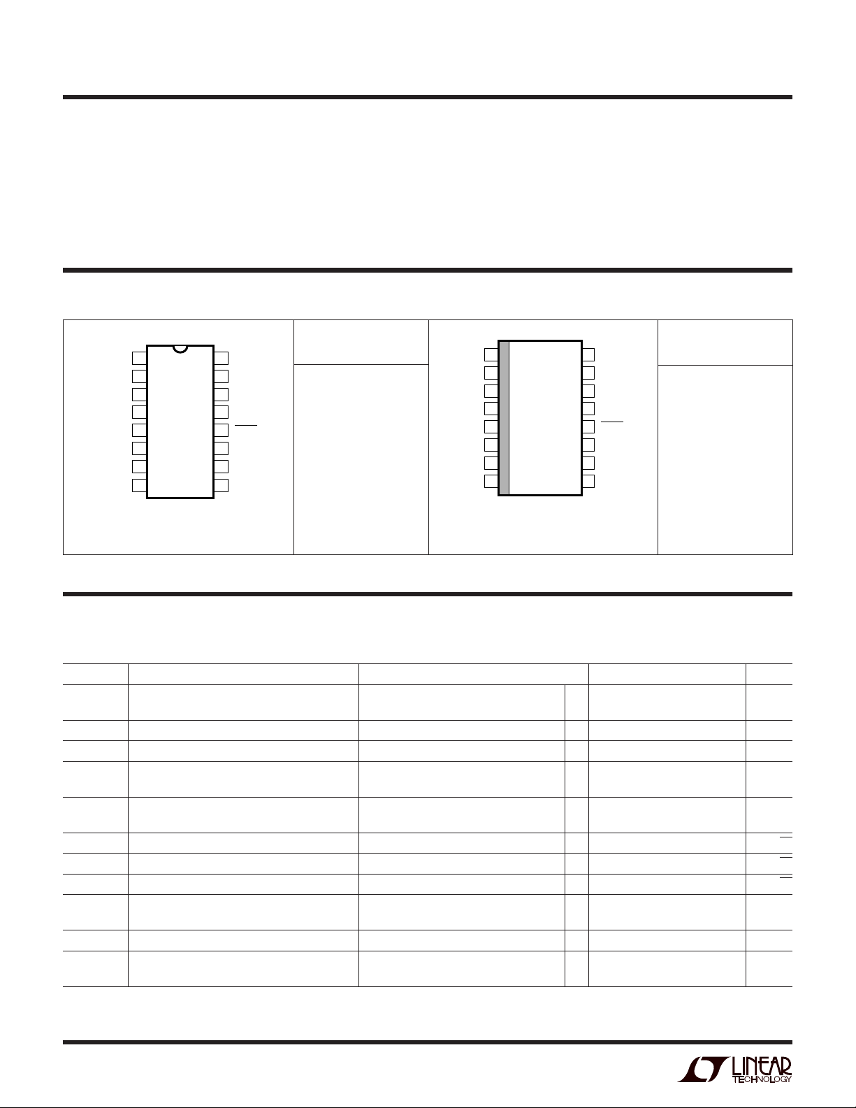
PACKAGE
V
IN0
GND
V
IN1
GND
V
IN2
GND
V
IN3
REF
T
JMAX
O
RDER I FOR ATIO
TOP VIEW
1
2
3
4
5
6
7
8
N PACKAGE
16-LEAD PDIP
= 150°C, θJA = 70°C/W
16
15
14
13
12
11
10
9
+
V
V
O
–
V
FB
SHDN
ENABLE
A1
A0
ORDER PART
NUMBER
LT1204CN*
*See Note 3 *See Note 3
Operating Temperature Range............... –40°C to 85°C
Storage Temperature Range................ –65°C to 150°C
Junction Temperature (Note 4)............................ 150°C
Lead Temperature (Soldering, 10 sec)..................300°C
U
V
1
IN0
GND
2
V
3
IN1
GND
4
V
5
IN2
GND
6
V
7
IN3
REF
8
16-LEAD PLASTIC SO
T
JMAX
TOP VIEW
16
15
14
13
12
11
10
9
SW PACKAGE
= 150°C, θJA = 90°C/W
+
V
V
O
–
V
FB
SHDN
ENABLE
A1
A0
ORDER PART
NUMBER
LT1204CSW*
Consult factory for Industrial and Military grade parts.
LECTRICAL C CHARA TERIST
E
ICS
0°C ≤ TA ≤ 70°C, ±5V ≤ VS ≤ ±15V, VCM = 0V, Pin 8 grounded and pulse tested unless otherwise noted.
SYMBOL PARAMETER CONDITIONS MIN TYP MAX UNITS
V
I
I
e
+i
–i
C
C
R
OS
IN
IN
n
IN
OUT
+
–
n
n
IN
Input Offset Voltage Any Positive Input, TA = 25°C514mV
● 16 mV
Offset Matching Between Any Positive Input, VS = ±15V ● 0.5 5 mV
Input Offset Voltage Drift Any Positive Input ● 40 µV/°C
Positive Input Bias Current Any Positive Input, TA = 25°C38µA
● 10 µA
Negative Input Bias Current TA = 25°C ±20 ±100 µA
● ±150 µA
Input Noise Voltage f = 1kHz, RF = 1k, RG = 10Ω, RS = 0Ω 7 nV/√Hz
Noninverting Input Noise Current Density f = 1kHz 1.5 pA/√Hz
Inverting Input Noise Current Density f = 1kHz 40 pA/√Hz
Input Capacitance Input Selected 3.0 pF
Input Deselected 3.5 pF
Output Capacitance Disabled, Pin 11 Voltage = 0V 8 pF
Positive Input Resistance, Any Positive Input VS = ±5V, VIN = –1.5V, 2V, TA = 25°C520 MΩ
= ±15V, VIN = ±5V ● 420 MΩ
V
S
2
Page 3
LT1204
LECTRICAL C CHARA TERIST
E
0°C ≤ TA ≤ 70°C, ±5V ≤ VS ≤ ±15V, VCM = 0V, Pin 8 grounded and pulse tested unless otherwise noted.
SYMBOL PARAMETER CONDITIONS MIN TYP MAX UNITS
Input Voltage Range, Any Positive Input VS = ±5V, TA = 25°C 2.0 2.5 V
CMRR Common Mode Rejection Ratio VS = ±5V, VCM = –1.5V, 2V, TA = 25°C4855 dB
Negative Input Current VS = ±5V, VCM = –1.5V, 2V, TA = 25°C 0.05 1 µA/V
Common Mode Rejection V
PSRR Power Supply Rejection Ratio VS = ±4.5V to ±15V ● 60 76 dB
Negative Input Current Power Supply Rejection VS = ±4.5V to ±15V ● 0.5 5 µA/V
A
R
V
I
I
VOL
OL
OUT
OUT
S
Large-Signal Voltage Gain VS = ±15V, V
Transresistance VS = ±15V, V
∆V
Output Voltage Swing VS = ±15V, RL = 400Ω, TA = 25°C ±12 ±13.5 V
Output Current RL = 0Ω, TA = 25°C 35 55 125 mA
Supply Current (Note 5) Pin 11 = 5V ● 19 24 mA
Disabled Output Resistance VS = ±15V, Pin 11 = 0V, VO = ±5V,
–
/∆I
O
IN
ICS
–1.5 –2.0 V
VS = ±15V ● ±5.0 ±6.0 V
= ±15V, Pin 8 Voltage = –5V ● 3.75 4.0 V
V
S
V
= ±15V, VCM = ±5V ● 48 58 dB
S
= ±15V, VCM = ±5V ● 0.05 1 µA/V
S
= ±10V, RL = 1k ● 57 73 dB
= ±5V, V
V
S
VS = ±5V, V
VS = ±5V, RL = 150Ω, TA = 25°C ±3.0 ±3.7 V
Pin 11 = 0V
Pin 12 = 0V
R
= RG = 1k ● 14 25 kΩ
F
VS = ±15V, Pin 11 = 0V, VO = ±5V,
R
= 2k, RG = 222Ω ● 820 kΩ
F
OUT
= ±2V, RL = 150Ω ● 57 66 dB
OUT
= ±10V, RL = 1k ● 115 310 kΩ
OUT
= ±2V, RL = 150Ω ● 115 210 kΩ
OUT
● ±10 V
● ±2.5 V
● 19 24 mA
● 1.5 3.5 mA
U
DIGITAL I PUT CHARACTERISTICS
0°C ≤ TA ≤ 70°C, VS = ±15V, RF = 2k, RG = 220Ω, RL = 400Ω unless otherwise noted.
SYMBOL PARAMETER CONDITIONS MIN TYP MAX UNITS
V
IL
V
IH
I
IL
I
IH
I
SHDN
t
sel
t
dis
t
en
t
SHDN
Input Low Voltage Pins 9, 10, 11, 12 ● 0.8 V
Input High Voltage Pins 9, 10, 11, 12 ● 2V
Input Low Current Pins 9, 10 Voltage = 0V ● 1.5 6 µA
Input High Current Pins 9, 10 Voltage = 5V ● 10 150 nA
Enable Low Input Current Pin 11 Voltage = 0V ● 4.5 15 µA
Enable High Input Current Pin 11 Voltage = 5V ● 200 300 µA
Shutdown Input Current Pin 12 Voltage 0V ≤ V
Channel-to-Channel Select Time (Note 6) Pin 8 Voltage = –5V, TA = 25°C 120 240 ns
Disable Time (Note 7) Pin 8 Voltage = –5V, TA = 25°C 40 100 ns
Enable Time (Note 8) Pin 8 Voltage = –5V, TA = 25°C 110 200 ns
Shutdown Assert or Release Time (Note 9) Pin 8 Voltage = –5V, TA = 25°C 1.4 10 µs
≤ 5V ● 20 80 µA
SHDN
3
Page 4

LT1204
AC CHARACTERISTICS
SYMBOL PARAMETER CONDITIONS MIN TYP MAX UNITS
tr, t
f
SR Slew Rate (Note 10) RL = 400Ω 400 1000 V/µs
t
S
The ● denotes specifications which apply over the specified operating
temperature range.
Note 1: Analog and digital inputs (Pins 1, 3, 5, 7, 9, 10, 11 and 12) are
protected against ESD and overvoltage with internal SCRs. For inputs
< ±6V the SCR will not fire, voltages above 6V will fire the SCRs and
the DC current should be limited to 50mA. To turn off the SCR the pin
voltage must be reduced to less than 2V or the current reduced to less
than 10mA.
Note 2: A heat sink may be required depending on the power supply
voltage.
Note 3: Commercial grade parts are designed to operate over the
temperature range of –40°C to 85°C but are neither tested nor
guaranteed beyond 0°C to 70°C. Industrial grade parts specified and
tested over –40°C to 85°C are available on special request. Consult
factory.
Note 4: T
dissipation P
LT1204CN: T
LT1204CS: T
Note 5: The supply current of the LT1204 has a negative temperature
coefficient. For more information see Typical Performance
Characteristics.
Note 6: Apply 0.5V DC to Pin 1 and measure the time for the
appearance of 5V at Pin 15 when Pin 9 goes from 5V to 0V. Pin 10
Voltage = 0V. Apply 0.5V DC to Pin 3 and measure the time for the
appearance of 5V at Pin 15 when Pin 9 goes from 0V to 5V. Pin 10
Voltage = 0V. Apply 0.5V DC to Pin 5 and measure the time for the
Small-Signal Rise and Fall Time RL = 150Ω, V
Channel Select Output Transient All VIN = 0V, RL = 400Ω, Input Referred 40 mV
Settling Time 0.1%, V
All Hostile Crosstalk (Note 11) SO PCB #028, RL = 100Ω, RS = 10Ω 92 dB
Disable Crosstalk (Note 11) SO PCB #028, Pin 11 Voltage = 0V, RL = 100Ω, RS = 50Ω 95 dB
Shutdown Crosstalk (Note 11) SO PCB #028, Pin 12 Voltage = 0V, RL = 100Ω, RS = 50Ω 92 dB
All Hostile Crosstalk (Note 11) PDIP PCB #029, RL = 100Ω, RS = 10Ω 76 dB
Disable Crosstalk (Note 11) PDIP PCB #029, Pin 11 Voltage = 0V, RL = 100Ω, RS = 50Ω 81 dB
Shutdown Crosstalk (Note 11) PDIP PCB #029, Pin 12 Voltage = 0V, RL = 100Ω, RS = 50Ω 76 dB
Differential Gain (Note 12) VS = ±15V, RL = 150Ω 0.04 %
Differential Phase (Note 12) VS = ±15V, RL = 150Ω 0.06 DEG
is calculated from the ambient temperature TA and power
J
according to the following formulas:
D
= TA + (PD)(70°C/W)
J
= TA + (PD)(90°C/W)
J
TA = 25°C, VS = ±15V, RF = RG = 1k, unless otherwise noted.
= ±125mV 5.6 ns
OUT
= 10V, RL = 1k 70 ns
OUT
= ±5V, RL = 150Ω 0.04 %
V
S
= ±5V, RL = 150Ω 0.12 DEG
V
S
appearance of 5V at Pin 15 when Pin 9 goes from 5V to 0V. Pin 10
Voltage = 5V. Apply 0.5V DC to Pin 7 and measure the time for the
appearance of 5V at Pin 15 when Pin 9 goes from 0V to 5V. Pin 10
Voltage = 5V.
Note 7: Apply 0.5V DC to Pin 1 and measure the time for the
disappearance of 5V at Pin 15 when Pin 11 goes from 5V to 0V.
Pins 9 and 10 are at 0V.
Note 8: Apply 0.5V DC to Pin 1 and measure the time for the
appearance of 5V at Pin 15 when Pin 11 goes from 0V to 5V.
Pins 9 and 10 are at 0V. Above a 1MHz toggle rate, t
Note 9: Apply 0.5V DC at Pin 1 and measure the time for the
appearance of 5V at Pin 15 when Pin 12 goes from 0V to 5V.
Pins 9 and 10 are at 0V. Then measure the time for the disappearance
of 5V DC to 500mV at Pin 15 when Pin 12 goes from 5V to 0V.
Note 10: Slew rate is measured at ±5V on a ±10V output signal while
operating on ±15V supplies with R
Note 11: VIN = 0dBm (0.223V
4th input selected. For Disable crosstalk and Shutdown crosstalk all 4
inputs are driven simultaneously. A 6dB output attenuator is formed by
a 50Ω series output resistor and the 50Ω input impedance of the
HP4195A Network Analyzer. R
Note 12: Differential Gain and Phase are measured using a Tektronix
TSG120 YC/NTSC signal generator and a Tektronix 1780R Video
Measurement Set. The resolution of this equipment is 0.1% and 0.1°.
Five identical MUXs were cascaded giving an effective resolution of
0.02% and 0.02°.
= 2k, RG = 220Ω and RL = 400Ω.
F
) at 10MHz on any 3 inputs with the
RMS
= RG = 1k.
F
reduces.
en
4
Page 5
U
W
TYPICAL AC PERFOR A CE
V
(V) A
S
±15 1 150 1.1k None 88.5 48.3 0.1
±12 1 150 976 None 82.6 49.1 0.1
±5 1 150 665 None 65.5 43.6 0.1
±15 2 150 787 787 75.7 45.8 0
±12 2 150 750 750 71.9 45.0 0
±5V 2 150 590 590 58.0 32.4 0
±15 10 150 866 95.3 44.3 28.7 0.1
±12 10 150 825 90.9 43.5 27.2 0
±5 10 150 665 73.2 37.2 22.1 0
V
RL (Ω)R
1k 1.6k None 95.6 65.8 0
1k 1.3k None 90.2 63.6 0.1
1k 866 None 68.2 42.1 0.1
1k 887 887 82.2 61.3 0.1
1k 845 845 77.5 52.1 0
1k 649 649 62.1 42.7 0.1
1k 1k 110 47.4 30.9 0.1
1k 931 100 46.3 32.1 0.1
1k 750 82.5 39.3 27.8 0.1
(Ω)R
F
Measurements taken from SO Demonstration Board #028.
SMALL SIGNAL SMALL SIGNAL SMALL SIGNAL
(Ω) –3dB BW (MHz) 0.1dB BW (MHz) PEAKING (dB)
G
LT1204
TRUTH TABLE
CHANNEL
A1 A0 ENABLE SHUTDOWN SELECTED
00 1 1 V
01 1 1 V
10 1 1 V
11 1 1 V
X X 0 1 High Z Output
X X X 0 Off
IN0
IN1
IN2
IN3
5
Page 6

LT1204
FREQUENCY (Hz)
1M
–2
GAIN (dB)
–1
0
1
2
10M 100M 1G
1204 G04
–3
–4
–5
–6
3
4
–120
PHASE (DEG)
–100
–80
–60
–40
–140
–160
–180
–200
–20
0
PHASE
GAIN
VS = ±5V
R
L
= 150Ω
R
F
= 655Ω
FREQUENCY (Hz)
1M
18
GAIN (dB)
19
20
21
22
10M 100M 1G
1204 G06
17
16
15
14
23
24
–120
PHASE (DEG)
–100
–80
–60
–40
–140
–160
–180
–200
–20
0
GAIN
VS = ±5V
R
L
= 150Ω
R
F
= 665Ω
R
G
= 73.2Ω
PHASE
LPER
UW
R
F
O
ATYPICA
CCHARA TERIST
E
C
ICS
±12V Frequency Response, AV = 1
4
3
2
1
0
–1
GAIN (dB)
–2
–3
–4
–5
–6
1M
PHASE
GAIN
10M 100M 1G
FREQUENCY (Hz)
VS = ±12V
= 150Ω
R
L
= 976Ω
R
F
1204 G01
0
–20
–40
–60
–80
–100
–120
–140
–160
–180
–200
PHASE (DEG)
±5V Frequency Response, AV = 1
±12V Frequency Response, AV = 2 ±5V Frequency Response, AV = 2
10
9
8
7
6
5
GAIN (dB)
4
3
2
1
0
1M
VS = ±12V
= 150Ω
R
GAIN
L
= 750Ω
R
F
= 750Ω
R
G
1204 G02
PHASE
10M 100M 1G
FREQUENCY (Hz)
0
–20
–40
–60
–80
–100
–120
–140
–160
–180
–200
PHASE (DEG)
10
9
8
7
6
5
GAIN (dB)
4
3
2
1
0
1M
PHASE
GAIN
10M 100M 1G
FREQUENCY (Hz)
VS = ±5V
= 150Ω
R
L
= 590Ω
R
F
= 590Ω
R
G
1204 G05
0
–20
–40
–60
–80
–100
–120
–140
–160
–180
–200
PHASE (DEG)
±12V Frequency Response, AV = 10
24
23
22
21
20
19
GAIN (dB)
18
17
16
15
14
1M
6
PHASE
GAIN
10M 100M 1G
FREQUENCY (Hz)
VS = ±12V
= 150Ω
R
L
= 825Ω
R
F
= 90.9Ω
R
G
1204 G03
0
–20
–40
–60
–80
–100
–120
–140
–160
–180
–200
±5V Frequency Response, AV = 10
PHASE (DEG)
Page 7

LPER
LT1204
UW
R
F
O
ATYPICA
CCHARA TERIST
E
C
ICS
Maximum Undistorted Output
vs Frequency
25
20
)
P-P
15
10
OUTPUT VOLTAGE (V
5
0
1
10 100
FREQUENCY (MHz)
±15V All Hostile Crosstalk
vs Frequency
–20
VS = ±15V
–30
= 100Ω
R
L
= RG = 1k
R
F
–40
= 0Ω
R
S
–50
DEMO PCB #028
–60
–70
–80
–90
–100
ALL HOSTILE CROSSTALK (dB)
–110
–120
1
CH1
CH3
CH2
10 100
FREQUENCY (MHz)
CH4
AV = 2AV = 1
VS = ±15V
= 1k
R
L
= 1k
R
FB
AV = 10
1204 G07
1204 G10
Maximum Capacitive Load
vs Feedback Resistor
10000
RL = 1k
= 2
A
V
T
= 25°C
A
≤ 5dB PEAKING
1000
VS = ±5V VS = ±15V
100
CAPACITIVE LOAD (pF)
10
023
1
FEEDBACK RESISTOR (kΩ)
1204 G08
±5V All Hostile Crosstalk
vs Frequency
–20
VS = ±5V
–30
= 100Ω
R
L
= RG = 1k
R
F
–40
= 0Ω
R
S
–50
DEMO PCB #028
–60
–70
–80
–90
–100
ALL HOSTILE CROSSTALK (dB)
–110
–120
1
ANY CHANNEL
10 100
FREQUENCY (MHz)
1204 G11
Total Harmonic Distortion
vs Frequency
0.1
VS = ±15V
= 400Ω
R
L
= RG = 1k
R
F
VO = 6V
0.01
TOTAL HARMONIC DISTORTION (%)
0.001
10
100 10k
RMS
VO = 1V
RMS
1k 100k
FREQUENCY (Hz)
All Hostile Crosstalk vs Frequency,
Various Source Resistance
–30
VS = ±15V
–40
= 100Ω
R
L
= RG = 1k
R
F
–50
DEMO PCB #028
–60
–70
–80
–90
–100
–110
ALL HOSTILE CROSSTALK (dB)
–120
–130
1
FREQUENCY (MHz)
RS = 37.5Ω
R
= 10Ω
S
= 0Ω
R
S
10 100
1204 G09
RS = 75Ω
1204 G12
Disable and Shutdown Crosstalk
vs Frequency
–20
VS = ±15V
–30
= 100Ω
R
L
= RG = 1k
R
F
–40
= 50Ω
R
S
–50
DEMO PCB #028
ALL CHANNELS DRIVEN
–60
–70
–80
–90
–100
ALL HOSTILE CROSSTALK (dB)
–110
–120
SHUTDOWN CROSSTALK
1
DISABLE CROSSTALK
10 100
FREQUENCY (MHz)
1204 G13
Spot Noise Voltage and Current
vs Frequency
100
–i
n
SPOT NOISE (nV/√Hz OR pA/√Hz)
10
1
10
100 10k
e
n
+i
n
1k 100k
FREQUENCY (Hz)
1204 G14
Amplifier Output Impedance
vs Frequency
1000
VS = ±15V
100
10
RFB = RG = 2k
1
OUTPUT IMPEDANCE (Ω)
RFB = RG = 750Ω
0.1
10k
100k
1M 100M
FREQUENCY (Hz)
10M
1204 G15
7
Page 8

LT1204
FREQUENCY (Hz)
20
POWER SUPPLY REJECTION (dB)
40
50
70
10k 1M 10M 100M
1204 G21
0
100k
60
30
10
–10
VS = ±15V
R
FB
= RG = 1k
POSITIVE
NEGATIVE
UW
TYPICAL PERFORMANCE CHARACTERISTICS
Output Disable V-I Characteristic
VS = ±15V
200
= RG = 1k
R
F
150
100
50
0
–50
–100
OUTPUT CURRENT (µA)
–150
–200
–3
–5
–4 4
SLOPE = 1/18k
–2
OUTPUT VOLTAGE (V)
–1
1
0
Input Voltage Range
vs Pin 8 Voltage
6
4
2
0
–2
INPUT VOLTAGE RANGE (V)
–4
–55°C, 25°C, 125°C
2
3
VS = ±15V
= 1
A
V
1204 G16
Disabled Output Impedance
vs Frequency
100
VS = ±15V
= RG = 1k
R
F
10
1
DISABLED OUTPUT IMPEDANCE (kΩ)
5
0
10k
1k 100k 1M 10M
FREQUENCY (Hz)
100M
1204 G17
Input Voltage Range
vs Supply Voltage
PIN 8 = 0V
6
4
25°C
2
0
–2
–55°C
INPUT VOLTAGE RANGE (V)
–4
–55°C
125°C
125°C
25°C
Maximum Channel Switching
Rate vs Pin 8 Voltage
0
–1
–2
–3
–4
–5
VOLTAGE ON PIN 8 (V)
–6
–7
–8
1.5 2.0 3.0
1.0
CHANNEL SWITCHING RATE (MHz)
2.5
Power Supply Rejection
vs Frequency
VIN = 1V
RL = 100Ω
= RG = 1k
R
FB
3.5
DC
4.0
1204 G18
–6
0
–2
–1 –3
–4
VOLTAGE ON PIN 8 (V)
Output Saturation Voltage
vs Temperature
+
V
RL = ∞
–0.5
–1.0
1.0
0.5
OUTPUT SATURATION VOLTAGE (V)
–
V
–50
–25 0
8
25 75
TEMPERATURE (°C)
–7
–5 –9
50 100 125
–6
–8
1204 G19
1204 G22
–6
2
4
6
8
SUPPLY VOLTAGE (±V)
12
10 16
Output Short-Circuit Current
vs Temperature
80
70
60
50
40
OUTPUT SHORT-CIRCUIT CURRENT (mA)
30
–50
–25
0
TEMPERATURE (°C)
50
25
75
14
100
1204 G20
1204 G23
125
Settling Time to 10mV
vs Output Step
10
VS = ±15V
8
= RG = 1k
R
F
6
4
2
0
–2
OUTPUT STEP (V)
–4
–6
–8
–10
40
30
SETTLING TIME (ns)
60
70
50
80
1204 G24
Page 9

LPER
SUPPLY VOLTAGE (±V)
0
0
SUPPLY CURRENT (mA)
1
15
16
17
22
19
4
8
10 18
1204 G27
2
20
21
18
26
12
14
16
25°C
125°C
–55°C
–55°C, 25°C, 125°C
I
SHDN
LT1204
UW
R
F
O
ATYPICA
CCHARA TERIST
E
C
ICS
Settling Time to 1mV
vs Output Step
10
VS = ±15V
8
= RG = 1k
R
F
6
4
2
0
–2
OUTPUT STEP (V)
–4
–6
–8
–10
PPLICATI
A
4
0
218
6
SETTLING TIME (µs)
12
10
8
U
O
S
14
16
20
1205 G25
I FOR ATIO
Enabled Supply Current
vs Supply Voltage
22
21
20
19
18
17
16
15
SUPPLY CURRENT (mA)
14
13
12
26
0
WU
U
–55°C
25°C
125°C
4
SUPPLY VOLTAGE (±V)
Logic Inputs
The logic inputs of the LT1204 are compatible with all 5V
logic. All pins have ESD protection (>2kV), and shorting
them to 12V or 15V will cause excessive currents to flow.
Limit the current to less than 50mA when driving the logic
above 6V.
Power Supplies
The LT1204 will operate from ±5V (10V total) to ±15V
(30V total) and is specified over this range. It is not
necessary to use equal value supplies, however, the offset
voltage and inverting input bias current will change. The
offset voltage changes about 600µV per volt of supply
mismatch. The inverting bias current changes about 2.5µA
per volt of supply mismatch. The power supplies should
be bypassed with quality tantalum capacitors.
Disabled and Shutdown Supply
Current vs Supply Voltage
14
10 18
8
16
12
1204 G26
specified over a very wide range of conditions. An advantage of the current feedback topology used in the LT1204
is well-controlled frequency response. In all cases of the
performance table, the peaking is 0.1dB or less. If more
peaking can be tolerated, larger bandwidths can be
obtained by lowering the feedback resistor. For gains of
2 or less, the 0.1dB bandwidth is greater than 30MHz for
all loads and supply voltages.
At high gains (low values of RG) the disabled output
resistance drops slightly due to loading of the internal
buffer amplifier as discussed in Multiplexer Expansion.
Small-Signal Rise Time, AV = 2
Feedback Resistor Selection
The small-signal bandwidth of the LT1204 is set by the
external feedback resistors and internal junction capacitors. As a result the bandwidth is a function of the supply
voltage, the value of the feedback resistor, the closedloop gain and the load resistor. These effects are outlined
in the resistor selection guide of the Typical AC Performance table. Bandwidths range as high as 95MHz and are
VS = ±15V
= 150Ω
R
L
R
= 1k
F
= 1k
R
G
1204 AI01
9
Page 10
LT1204
PPLICATI
A
U
O
S
I FOR ATIO
WU
U
Capacitance on the Inverting Input
Current feedback amplifiers require resistive feedback
from the output to the inverting input for stable operation.
Take care to minimize the stray capacitance between the
output and the inverting input. Capacitance on the inverting input to ground will cause peaking in the frequency
response and overshoot in the transient response.
Capacitive Loads
The LT1204 can drive capacitive loads directly when the
proper value of feedback resistor is used. The graph of
Maximum Capacitive Load vs Feedback Resistor should
be used to select the appropriate value. The value shown
is for 5dB peaking when driving a 1k load at a gain of 2.
This is a worst-case condition. The amplifier is more
stable at higher gains and driving heavier loads. Alternatively, a small resistor (10Ω to 20Ω) can be put in series
with the output to isolate the capacitive load from the
amplifier output. This has the advantage that the amplifier bandwidth is only reduced when the capacitive load
is present. The disadvantage is that the gain is a function
of load resistance.
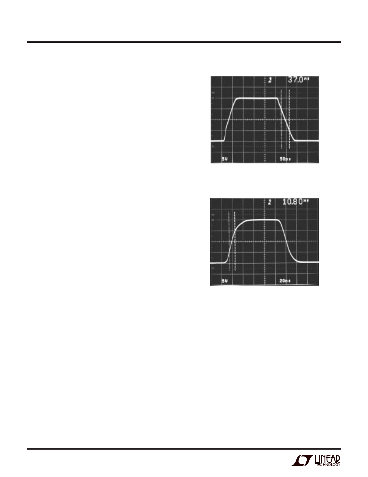
Large-Signal Transient Response
VS = ±15V
= 2
A
V
= 1k
R
F
= 1k
R
G
R
= 400Ω
L
Large-Signal Transient Response
1204 AI02
Slew Rate
The slew rate of the current feedback amplifier on the
LT1204 is not independent of the amplifier gain the way
slew rate is in a traditional op amp. This is because both the
input and the output stage have slew rate limitations. In
high gain settings the signal amplitude between the negative input and any driven positive input is small and the
overall slew rate is that of the output stage. For gains less
than 10, the overall slew rate is limited by the input stage.
The input slew rate of the LT1204 is approximately 135V/µs
and is set by internal currents and capacitances. The
output slew rate is set by the value of the feedback
resistors and the internal capacitances. At a gain of 10 with
a 1k feedback resistor and ±15 supplies, the output slew
rate is typically 1000V/µs. Larger feedback resistors will
reduce the slew rate as will lower supply voltages, similar
to the way the bandwidth is reduced.
The graph, Maximum Undistorted Output vs Frequency,
relates the slew rate limitations to sinusoidal inputs for
various gain configurations.
V
= ±15V
S
= 10
A
V
= 910Ω
R
F
= 100Ω
R
G
R
= 400Ω
L
1204 AI03
Switching Characteristics and Pin 8
Switching between channels is a “make-before-break”
condition where both inputs are on momentarily. The
buffers isolate the inputs when the “make-before-break”
switching occurs. The input with the largest positive
voltage determines the output level. If both inputs are
equal, there is only a 40mV error at the input of the CFA
during the transition. The reference adjust (Pin 8) allows
the user to trade off positive input voltage range for
switching time. For example, on ±15V supplies, setting
the voltage on Pin 8 to –6.8V reduces the switching
transient to a 50ns duration, and reduces the positive input
range from 6V to 2.35V. The negative input range remains
unchanged at –6V. When switching video “in picture,” this
short transient is imperceptible even on high quality
10
Page 11

LT1204
PPLICATI
A
U
O
S
I FOR ATIO
WU
U
monitors. The reference pin has no effect when the LT1204
is operating on ±5V, and should be grounded. On supply
voltages above ±8V, the range of voltages for Pin 8 should
be between – 6.5V and – 7.5V. Reducing Pin 8 voltage
below – 7.5V turns “on” the “off” tee switch, and the
isolation between channels is lost.
Channel-to-Channel Switching
A0 PIN 9
V
PIN 15
OUT
V
IN0
PIN 8 VOLTAGE = –6.8V, V
A0 PIN 9
AND V
CONNECTED TO 2MHz SINEWAVE
IN1
S
Transient at Input Buffer
= ±15V
1204 AI04
Competitive MUXs
CMOS MUX
BIPOLAR
MUX
V
IN0
AND V
CONNECTED TO 2MHz SINEWAVE
IN1
1204 AI06
Crosstalk
The crosstalk, or more accurately all hostile crosstalk, is
measured by driving a signal into any three of the four
inputs and selecting the 4th input with the logic control.
This 4th input is either shorted to ground or terminated in
an impedance. All hostile crosstalk is defined as the ratio
in decibel of the signal at the output of the CFA to the signal
on the three driven inputs, and is input-referred. Disable
crosstalk is measured with all four inputs driven and the
part disabled. Crosstalk is critical in many applications
where video multiplexers are used. In professional video
systems, a crosstalk figure of –72dB is a desirable
specification.
V
PIN 1
IN0
SWITCHING BETWEEN V
RS = 50Ω, V
= –6.8V, VS ±15V
REF
IN0
AND V
IN1
1204AI05
Competitive video multiplexers built in CMOS are bidirectional and suffer from poor output-to-input isolation and
cause transients to feed to the inputs. CMOS MUXs have
been built with “break-before-make” switches to eliminate
the talking between channels, but these suffer from output
glitches large enough to interfere with sync circuitry.
Multiplexers built on older bipolar processes that switch
lateral PNP transistors take several microseconds to settle
and blur the transition between pictures.
The key to the outstanding crosstalk performance of the
LT1204 is the use of tee switches (see Figure 1). When the
tee switch is on (Q2 off) Q1 and Q3 are a pair of emitter
followers with excellent AC response for driving the CFA.
+
V
I
1
Q3
V
IN0
TO LOGIC
Q1
Q2
–
V
I
2
–V
+
CFA
V
OUT
–
R
FB
R
G
F
1204 F01
Figure 1. Tee Switch
11
Page 12

LT1204
PPLICATI
A
U
O
S
I FOR ATIO
WU
U
When the decoder turns off the tee switch (Q2 on) the
emitter base junctions of Q1 and Q3 become reversebiased while Q2 emitter absorbs current from I1. Not only
do the reverse-biased emitter base junctions provide good
isolation, but any signal at V
coupling to Q1 emitter is
IN0
further attenuated by the shunt impedance of Q2 emitter.
Current from I2 is routed to any on switch.
Crosstalk performance is a strong function of the IC
package, the PC board layout as well as the IC design. The
die layout utilizes grounds between each input to isolate
adjacent channels, while the output and feedback pins are
on opposite sides of the die from the input. The layout of
a PC board that is capable of providing –90dB all hostile
crosstalk at 10MHz is not trivial. That level corresponds to
a 30µV output below a 1V input at 10MHz. A demonstra-
tion board has been fabricated to show the component and
ground placement required to attain these crosstalk num-
All Hostile Crosstalk
–20
V
= ±15V
S
= GND
V
IN0
= 0dBm
V
IN1,2,3
–40
= 100Ω
R
L
–60
–80
–100
ALL HOSTILE CROSSTALK (dB)
–120
1
DEMO PCB #029
PDIP
SO
DEMO PCB #028
10 100
FREQUENCY (MHz)
1204 AI07
bers. A graph of all hostile crosstalk for both the PDIP and
SO packages is shown. It has been found empirically from
these PC boards that capacitive coupling across the package of greater than 3fF (0.003pF) will diminish the rejection, and it is recommended that this proven layout be
copied into designs. The key to the success of the SO PC
board #028 is the use of a ground plane guard around Pin
13, the feedback pin.
PDIP PC Board #029, Component Side
GND V– V+
VOUT
VIN0
U1
VIN1
VIN2
R1
VIN3
C1
C2
+
C3
+
RF
C4
R6
R2
(408) 432-1900
LT1204 VIDEO MUX
DEMONSTRATION BOARD
RO
ENABLE
R1
R3
R0
S/D
REF
1204 AI09
12
Page 13

LT1204
PPLICATI
A
U
O
S
I FOR ATIO
GND V+
WU
SOL PC Board #028, Component Side
U
V–
VIN0
C2
C4
VOUT
ENABLE
VIN1
VIN2
C1
U1
RO
RF
C3
RG
R2
R1
(408) 432-1900
LT1204 VIDEO MUX
DEMONSTRATION BOARD
A1
R3
A0
S/D
VIN3
REF
1204 AI08
13
Page 14

LT1204
PPLICATI
A
U
O
S
I FOR ATIO
1
V
IN0
V
IN1
V
IN2
V
IN3
V
2
GND
3
V
4
GND
5
V
6
GND
7
V
8
REF
WU
Demonstration PC Board Schematic
GND
16
+
LT1204
V
SHDN
ENABLE
V
15
O
14
–
V
13
FB
12
11
10
A1
A0
IN0
IN1
IN2
IN3
9
–
V
U
+
V
R1
10kR210k
+
C1
4.7µF
C3
+
4.7µF
R3
10k
L1204 AI10
C2
0.1µF
C4
0.1µF
SHUTDOWN
ENABLE
A1
A0
REF
R
O
75Ω
R
F
R
G
750Ω
750Ω
RESISTORS R1, R2 AND R3 ARE PULL-DOWN
AND PULL-UP RESISTORS FOR THE LOGIC
AND ENABLE PINS. THEY MAY BE OMITTED
IF THE LT1204 IS DRIVEN FROM TTL LEVELS
OR FROM 5V CMOS.
All Hostile Crosstalk Test Setup*
HP4195A
NETWORK ANALYZER
OSC REF V
50Ω
10Ω
50Ω
50Ω
SPLITTER
1
V
2
GND
3
V
4
GND
5
V
6
GND
7
V
8
REF
50Ω 50Ω
IN0
IN1
LT1204
IN2
ENABLE
IN3
V
V
V
FB
SHDN
A1
A0
Alternate All Hostile Crosstalk Setup*
HP4195A
NETWORK ANALYZER
IN
16
+
15
O
14
–
–15V
13
12
11
10
9
15V
50Ω
1k
1k
10k
*SEE PC BOARD LAYOUT
1204 AI11
OSC REF V
50Ω
50Ω
SPLITTER
50Ω
50Ω
50Ω
50Ω 50Ω
10Ω
IN
SHDN
ENABLE
16
+
V
15
V
O
14
–
V
FB
A1
A0
–15V
13
12
11
10
9
15V
50Ω
1k
1k
10k
*SEE PC BOARD LAYOUT
1204 AI12
1
V
IN0
2
GND
3
V
IN1
4
GND
LT1204
5
V
IN2
6
GND
7
V
IN3
8
REF
14
Page 15

LT1204
PPLICATI
A
U
O
S
I FOR ATIO
WU
U
Multiplexer Expansion Pin 11 and Pin 12
To expand the number of MUX inputs, LT1204s can be
paralleled by shorting their outputs together. The multiplexer disable logic has been designed to prevent shootthrough current when two or more amplifiers have their
outputs shorted together. (Shoot-through current is a
spike of power supply current caused by both amplifiers
being on at once.)
Monitoring Supply Current Spikes
+
V
5V
O
OSCILLATOR
10mA/DIV
OSCILLATOR
74HC04
OUTPUT
5V/DIV
5V/DIV
V
OUT
1V/DIV
TEK
CT-1
1
+
3
+
5
+
7
+
13
–
V
1k
1k
V
1
+
3
+
5
+
7
+
13
–
V
1k
Timing and Supply Current Waveforms
I
S
LT1204
EN
14
–
+
16
EN
LT1204
14
–
1k
16
11
11
TO SCOPE
15
74HC04
15
75Ω
75Ω
75Ω
1204 AI13
1204 AI14
The multiplexer uses a circuit to ensure the disabled
amplifiers do not load or alter the cable termination. When
the LT1204 is disabled (Pin 11 low) the output stage is
turned off and an active buffer senses the output and
drives the feedback pin to the CFA (Figure 2). This bootstraps the feedback resistors and raises the true output
impedance of the circuit. For the condition where RF = R
G
= 1k, the Disable Output Resistance is typically raised to
25k and drops to 20k for AV = 10, RF = 2k and RG = 222Ω
due to loading of the feedback buffer. Operating the
Disable feature with RG < 100Ω is not recommended.
IN0
IN1
IN2
IN3
TEE SWITCHV
TEE SWITCHV
AV = +1
+
TEE SWITCHV
CFA
“OFF”
–
TEE SWITCHV
FB
R
G
–
V
LT1204
“ON”
R
F
Figure 2. Active Buffer Drives FB Pin 13
V
OUT
75Ω
CABLE
75Ω
75Ω
1204 F02
A shutdown feature (Pin 12 low) reduces the supply
current to 1.5mA and lowers the power dissipation
when the LT1204 is not in use. If the part is shut down,
the bootstrapping is inoperative and the feedback resistors will load the output. If the CFA is operated at a gain
of +1, however, the feedback resistor will not load the
output even in shutdown because there is no resistive
path to ground, but there will be a –6dB loss through
the cable system.
A frequency response plot shows the effect of using the
disable feature versus using the shutdown feature. In
this example four LT1204s were connected together at
their outputs forming a 16-to-1 MUX. The plot shows the
effect of the bootstrapping circuit that eliminates the
15
Page 16

LT1204
PPLICATI
A
U
O
S
I FOR ATIO
WU
U
improper cable termination due to feedback resistors
loading the cable.
The limit to the number of expanded inputs is set by the
acceptable error budget of the system.
16-to-1 MUX Response Using Disable vs Shutdown
4
VS = ±15V
R
= 100Ω
L
= RG = 1k
R
F
2
0
GAIN (dB)
–2
–4
–6
1
16-to-1 Multiplexer All Hostile Crosstalk
–20
VS = ±15V
= 100Ω
R
L
R
= RG = 1k
F
–40
= 0
R
S
–60
–80
DISABLE
SHUTDOWN
10 100
FREQUENCY (MHz)
SHUTDOWN
CROSSTALK
1204 AI15
For a 64-to-1 MUX we need sixteen LT1204s. The
equivalent load resistance due to the feedback resistor
REQ in Disable is 25k/15 = 1.67k. See Figure 3.
75R
VO =
75(75) + 150R
EQ
, VO = 0.489V
EQ
This voltage represents a 2.1% loading error. If the
shutdown feature is used instead of the disable feature,
then the LT1204 could expand to only an 8-to-1 MUX for
the same error.
As a practical matter the gain error at frequency is also
set by capacitive loading. The disabled output capacitance of the LT1204 is about 8pF, and in the case of
sixteen LT1204s, it would represent a 128pF load. The
combination of 1.67k and 128pF correspond to about a
0.3dB roll-off at 5MHz.
OFF
LT1204
ON
LT1204
75Ω
CABLE
75Ω
1V
V
OUT
75Ω
16
–100
ALL HOSTILE CROSSTALK (dB)
–120
1
FREQUENCY (MHz)
DISABLE
CROSSTALK
10 100
1204 AI16
75Ω
1V
R
EQ
V
OUT
75Ω
1204 F03
Figure 3. Equivalent Loading Schematic
Page 17

LT1204
U
O
PPLICATITYPICAL
SA
Programable Gain Amplifier (PGA)
Two LT1204s and seven resistors make a Programable
Gain Amplifier with a 128-to-1 gain range. The gain is
proportional to 2N where N is the 3-bit binary value of the
select logic. An input attenuator alters the input signal
Programable Gain Amplifier Accepts Inputs
VIN = 62.5mV
499Ω
P-P
TO 8V
249Ω
P-P
from 62.5mV
124Ω
124Ω
P-P
1
3
5
7
13
100Ω
1
3
5
7
13
to 8V
+
+
LT1204
+
#1
+
–
+
+
LT1204
+
#2
+
–
P-P
1.5k
1.5k
V
1204 TA03
OUT
= 1V
P-P
by 1, 0.5, 0.25 and 0.125 to form an amplifier with a gain
of 16, 8, 4, 2, when LT1204 #1 is selected. LT1204 #2
is connected to the same attenuator. When enabled
(LT1204 #1 disabled), it results in gain of 1, 0.5, 0.25 and
0.125. The wide input common mode range of the
LT1204 is needed to accept inputs of 8V
P-P
.
4-Input Differential Receiver
LT1204s can be connected inverting and noninverting as
shown to make a 4-input differential receiver. The receiver
can be used to convert differential signals sent over a low
cost twisted pair to a single-ended output or used in video
loop-thru connections. The logic inputs A0 and A1 are tied
together because the same channels are selected on each
LT1204. By using the Disable feature, the number of
differential inputs can be increased by adding pairs of
LT1204s and tying the outputs of the noninverting LT1204s
(#1) together. Switching transients are reduced in this
receiver because the transient from LT1204 #2 subtracted
from the transient of LT1204 #1.
TWISTED PAIR
CABLE
*OPTIONAL
4-Input Differential Receiver
IN 1
1k*
1k*
IN 2
IN 3
IN 4
–IN 1
–IN 2
–IN 3
–IN 4
68Ω
68Ω
1k*
1k*
ENSHDNA1A0
+
A0
A1
+
SHDN
+
+
LT1204
EN
#1
–
1k
1k
+
A0
A1
+
SHDN
+
+
LT1204
EN
#2
75Ω
V
OUT
75Ω
–
1k
1k
1204 TA04
17
Page 18

LT1204
U
O
PPLICATITYPICAL
SA
Differential Receiver Switching Waveforms
CABLE
OUTPUT
LT1204
#2 OUTPUT
A0 PIN 9
1204 TA05
4-Input Twisted-Pair Driver
It is possible to send and receive color composite video
signals appreciable distances on a low cost twisted pair.
The cost advantage of this technique is significant. Standard 75Ω RG-59/U coaxial cable cost between 25¢ and
50¢ per foot. PVC twisted pair is only pennies per foot.
Differential signal transmission resists noise because the
interference is present as a common mode signal. The
LT1204 can select one of four video cameras for instance,
Differential Receiver Response
VS = ±15V
20
= 100Ω
R
L
DIFFERENTIAL MODE RESPONSE
0
–20
–40
–60
DIFFERENTIAL RECEIVER RESPONSE (dB)
10k 1M 10M 100M
COMMON MODE RESPONSE
100k
FREQUENCY (Hz)
1204 TA06
and drive the video signal on to the twisted pair. The circuit
uses an LT1227 current feedback amplifier connected with
a gain of –2, and an LT1204 with a gain of 2. The 47Ω
resistors back-terminate the low cost cable in its characteristic impedance to prevent reflections. The receiver for
the differential signal is an LT1193 connected for a gain of
2. Resistors R1, R2 and capacitors C1, C2 are used for
cable compensation for loss through the twisted pair.
Alternately, a pair of LT1204s can be used to perform the
differential to single-ended conversion.
Multiburst Pattern Passed Through 1000 Feet of Twisted Pair,
No Cable Compensation
INPUT
OUTPUT
1204 TA08
Multiburst Pattern Passed Through 1000 Feet of Twisted Pair,
with Cable Compensation
INPUT
OUTPUT
1204 TA09
18
Page 19

PACKAGE DESCRIPTIO
U
Dimensions in inches (millimeters) unless otherwise noted.
N Package
16-Lead PDIP (Narrow 0.300)
(LTC DWG # 05-08-1510)
0.770*
(19.558)
MAX
12
13
4
11
6
5
7
0.255 ± 0.015*
(6.477 ± 0.381)
14
15
16
2
1
3
LT1204
910
8
0.300 – 0.325
(7.620 – 8.255)
0.009 – 0.015
(0.229 – 0.381)
+0.035
0.325
–0.015
+0.889
8.255
()
–0.381
*THESE DIMENSIONS DO NOT INCLUDE MOLD FLASH OR PROTRUSIONS.
MOLD FLASH OR PROTRUSIONS SHALL NOT EXCEED 0.010 INCH (0.254mm)
0.020
(0.508)
MIN
0.130 ± 0.005
(3.302 ± 0.127)
0.125
(3.175)
MIN
0.100 ± 0.010
(2.540 ± 0.254)
SW Package
16-Lead Plastic Small Outline (Wide 0.300)
(LTC DWG # 05-08-1620)
NOTE 1
0.045 – 0.065
(1.143 – 1.651)
0.398 – 0.413*
(10.109 – 10.490)
15 1413121110 9
16
0.065
(1.651)
TYP
0.018 ± 0.003
(0.457 ± 0.076)
N16 1197
0.394 – 0.419
(10.007 – 10.643)
2345
0.093 – 0.104
0.050
(1.270)
TYP
1
0.014 – 0.019
(0.356 – 0.482)
TYP
0.291 – 0.299**
(7.391 – 7.595)
0.010 – 0.029
(0.254 – 0.737)
0.009 – 0.013
(0.229 – 0.330)
NOTE:
1. PIN 1 IDENT, NOTCH ON TOP AND CAVITIES ON THE BOTTOM OF PACKAGES ARE THE MANUFACTURING OPTIONS.
THE PART MAY BE SUPPLIED WITH OR WITHOUT ANY OF THE OPTIONS
DIMENSION DOES NOT INCLUDE MOLD FLASH. MOLD FLASH SHALL NOT EXCEED 0.006" (0.152mm) PER SIDE
*
DIMENSION DOES NOT INCLUDE INTERLEAD FLASH. INTERLEAD FLASH SHALL NOT EXCEED 0.010" (0.254mm) PER SIDE
**
NOTE 1
Information furnished by Linear Technology Corporation is believed to be accurate and reliable.
However, no responsibility is assumed for its use. Linear Technology Corporation makes no represen-
× 45°
0.016 – 0.050
(0.406 – 1.270)
° – 8° TYP
0
(2.362 – 2.642)
tation that the interconnection of its circuits as described herein will not infringe on existing patent rights.
6
78
0.037 – 0.045
(0.940 – 1.143)
0.004 – 0.012
(0.102 – 0.305)
S16 (WIDE) 0396
19
Page 20
LT1204
TYPICAL APPLICATION
V
IN0
V
75Ω
IN1
V
IN2
V
IN3
1k
U
+
+
+
+
–
–
LT1227
+
4-Input Twisted-Pair Driver/Receiver
LT1204
1k
2k
47Ω
47Ω
1000 FT OF
TWISTED PAIR
18Ω
390Ω
91Ω
300Ω
+
LT1193
–
75Ω
+
–
300Ω
1204 TA07
680pF
300pF
200Ω
RELATED PARTS
PART NUMBER DESCRIPTION COMMENTS
LT1203/LT1205 150MHz Video Multiplexer High Speed, but No Cable Driving
LT1259/LT1260 Dual and Triple Current Feedback Amplifiers Low Cost, with Shutdown
LT1675 RGB Multiplexer with Current Feedback Amplifiers Very High Speed, Pixel Switching
20
Linear Technology Corporation
1630 McCarthy Blvd., Milpitas, CA 95035-7417
(408) 432-1900 ● FAX: (408) 434-0507
●
www.linear-tech.com
1204fas, sn1204 LT/TP 0898 2K REV A • PRINTED IN USA
LINEAR TECHNOLOGY CORPORATION 1993
 Loading...