

Page 1
LT1187
FREQUENCY (MHz)
0
VOLTAGE GAIN (dB)
10
20
30
40
0.1 10 100
LT1187 • TA02
–10
1
VS = ±5V
R
L
= 1k
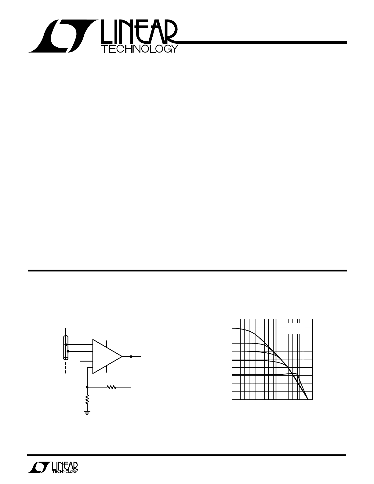
Low Power
Video Difference Amplifier
EATU
F
■
Differential or Single-Ended Gain Block (Adjustable)
■
–3dB Bandwidth, AV = ±2 50MHz
■
Slew Rate 165V/µs
■
Low Supply Current 13mA
■
Output Current ±20mA
■
CMRR at 10MHz 40dB
■
LT1193 Pin Compatible
■
Low Cost
■
Single 5V Operation
■
Drives Cables Directly
■
Output Shutdown
PPLICATI
A
■
Line Receivers
■
Video Signal Processing
■
Cable Drivers
■
Tape and Disc Drive Systems
RE
S
O
U
S
DUESCRIPTIO
The LT1187 is a difference amplifier optimized for operation on ± 5V, or a single 5V supply, and gain ≥ 2. This
versatile amplifier features uncommitted high input impedance (+) and (–) inputs, and can be used in differential
or single-ended configurations. Additionally, a second set
of inputs give gain adjustment and DC control to the
difference amplifier.
The LT1187’s high slew rate, 165V/µs, wide bandwidth,
50MHz, and ±20mA output current require only 13mA of
supply current. The shutdown feature reduces the power
dissipation to a mere 15mW, and allows multiple amplifiers to drive the same cable.
The LT1187 is a low power version of the popular LT1193,
and is available in 8-pin miniDIPs and SO packages. For
applications with gains of 10 or more, see the LT1189
data sheet.
CABLE
V
A
IN
PPLICATITYPICAL
with DC Adjust
V
DC
U
O
Closed-Loop Gain vs FrequencyCable Sense Amplifier for Loop Through Connections
5V
3
+
1k
–
LT1187
+
–
–5V
7
6
4
1k
V
LT1187 • TA01
OUT
2
1
8
1
Page 2
LT1187
WU
U
PACKAGE
/
O
RDER I FOR ATIO
W
O
A
LUTEXI T
S
Total Supply Voltage (V+ to V–) ............................. 18V
Differential Input Voltage ........................................ ±6V
Input Voltage .......................................................... ±V
Output Short Circuit Duration (Note 1) ........ Continuous
Operating Temperature Range
LT1187M..................................... –55°C to 150°C
LT1187C............................................. 0°C to 70°C
Junction Temperature (Note 2)
Plastic Package (CN8,CS8) ......................... 150°C
Ceramic Package (CJ8,MJ8) ....................... 175°C
Storage Temperature Range ................ – 65°C to 150°C
Lead Temperature (Soldering, 10 sec.)................ 300°C
+
5V
–
VS = ±5V, V
SYMBOL PARAMETER CONDITIONS MIN TYP MAX UNITS
V
OS
I
OS
I
B
e
n
i
n
R
IN
C
IN
VIN
LIM
CMRR Common-Mode Rejection Ratio VCM = –2.5V to 3.5V 70 100 dB
PSRR Power Supply Rejection Ratio VS = ±2.375V to ±8V 70 85 dB
V
OUT
G
E
SR Slew Rate (Note 6, 10) 100 165 V/µs
FPBW Full Power Bandwidth VO = 1V
BW Small Signal Bandwidth AV = 10 5.7 MHz
tr, t
f
t
PD
t
s
Diff A
Diff Ph Differential Phase RL = 1k, AV = 4, (Note 9) 0.8 DEG
I
S
LECTRICAL C CHARA TERIST
E
= 0V, R
REF
Input Offset Voltage Either Input, (Note 4) 2.0 10 mV
Input Offset Current Either Input 0.2 1.0 µA
Input Bias Current Either Input ±0.5 ±2.0 µA
Input Noise Voltage fO = 10kHz 65 nV/√Hz
Input Noise Current fO = 10kHz 1.5 pA/√Hz
Input Resistance Differential 100 kΩ
Input Capacitance Either Input 2.0 pF
Input Voltage Limit (Note 5) ±380 mV
Input Voltage Range –2.5 3.5 V
Output Voltage Swing VS = ±5V, RL = 1k, AV = 50 ±3.8 ±4.0 V
Gain Error VO = ±1V, AV = 10, RL = 1k 0.2 1.0 %
Rise Time, Fall Time AV = 50, VO = ±1.5V, 20% to 80% (Note 10) 150 230 325 ns
Propagation Delay RL= 1k, VO = ±125mV, 50% to 50% 26 ns
Overshoot VO = ±50mV 0 %
Settling Time 3V Step, 0.1%, (Note 8) 100 ns
V
Differential Gain RL = 1k, AV = 4, (Note 9) 0.6 %
Supply Current 13 16 mA
Shutdown Supply Current Pin 5 at V
A
= 900Ω from pins 6 to 8, R
FB1
WUW
U
ARB
G
S
I
TOP VIEW
1+/REF
S
8-LEAD HERMETIC DIP
Consult factory for Industrial grade parts.
ICS
TA = 25°C, (Note 3)
= 100Ω from pin 8 to ground, RL = R
FB2
SOIC Package 2.0 11 mV
VS = ±8V, RL = 1k, AV = 50 ±6.7 ±7.0
VS = ±8V, RL = 300Ω, AV = 50, (Note 3) ±6.4 ±6.8
, (Note 7) 53 MHz
P-P
–
2
–IN
+IN
3
–
V
J8 PACKAGE
8-LEAD PLASTIC SOIC
T
= 175°C, θJA = 100°C/W (J8)
JMAX
= 150°C, θJA = 100°C/W (N8)
T
JMAX
T
= 150°C, θJA = 150°C/W (S8)
JMAX
8-LEAD PLASTIC DIP
S8 PACKAGE
–/FB
8
7
V
6
OUT
54
S/D
N8 PACKAGE
LT1187 • POI01
+ R
FB1
+
= 1k, CL ≤ 10pF, pin 5 open.
FB2
ORDER PART
NUMBER
LT1187MJ8
LT1187CJ8
LT1187CN8
LT1187CS8
S8 PART MARKING
1187
LT1187M/C
0.8 1.5 mA
P-P
2
Page 3
LT1187
+
5V
–
VS = ±5V, V
SYMBOL PARAMETER CONDITIONS MIN TYP MAX UNITS
I
S/D
t
ON
t
OFF
LECTRICAL C CHARA TERIST
E
= 0V, R
REF
Shutdown Pin Current Pin 5 at V
Turn On Time Pin 5 from V– to Ground, RL = 1k 500 ns
Turn Off Time Pin 5 from Ground to V–, RL = 1k 600 ns
= 900Ω from pins 6 to 8, R
FB1
ICS
TA = 25°C, (Note 3)
= 100Ω from pin 8 to ground, RL = R
FB2
–
FB1
+ R
= 1k, CL ≤ 10pF, pin 5 open.
FB2
LT1187M/C
525 µA
5V
V
LECTRICAL C CHARA TERIST
E
+
= 5V, V
S
–
= 0V, V
S
= 2.5V, R
REF
= 900Ω from pins 6 to 8, R
FB1
ICS
open.
SYMBOL PARAMETER CONDITIONS MIN TYP MAX UNITS
V
OS
I
OS
I
B
CMRR Common-Mode Rejection Ratio VCM = 2.0V to 3.5V 70 100 dB
V
OUT
SR Slew Rate VO = 1.5V to 3.5V 130 V/µs
BW Small-Signal Bandwidth AV = 10 5.3 MHz
I
S
I
S/D
+
5V
–
VS = ±5V, V
SYMBOL PARAMETER CONDITIONS MIN TYP MAX UNITS
V
OS
∆VOS/∆T Input V
I
OS
I
B
CMRR Common-Mode Rejection Ratio VCM = –2.5V to 3.5V 70 100 dB
PSRR Power Supply Rejection Ratio VS = ±2.375V to ±8V 60 85 dB
V
OUT
G
E
I
S
I
S/D
Input Offset Voltage Either Input, (Note 4) 2.0 10 mV
SOIC Package 2.0 12 mV
Input Offset Current Either Input 0.2 1.0 µA
Input Bias Current Either Input ±0.5 ±2.0 µA
Input Voltage Range 2.0 3.5 V
Output Voltage Swing RL = 300Ω to Ground V
(Note 3)
Supply Current 12 15 mA
Shutdown Supply Current Pin 5 at V
Shutdown Pin Current Pin 5 at V
LECTRICAL C CHARA TERIST
E
= 0V, R
REF
Input Offset Voltage Either Input, (Note 4) 2.0 15 mV
Input Offset Current Either Input 0.2 1.5 µA
Input Bias Current Either Input ±0.5 ±3.5 µA
Input Voltage Range –2.5 3.5 V
Output Voltage Swing VS = ±5V, RL = 1k, AV = 50 ±3.7 ±4.0 V
Gain Error VO = ±1V, AV = 10, RL = 1k 0.2 1.2 %
Supply Current 13 17 mA
Shutdown Supply Current Pin 5 at V–, (Note 11) 0.8 1.5 mA
Shutdown Pin Current Pin 5 at V
= 900Ω from pins 6 to 8, R
FB1
Drift 8.0 µV/°C
OS
VS = ±8V, RL = 1k, AV = 50 ±6.6 ±7.0
VS = ±8V, RL = 300Ω, AV = 50, (Note 3) ±6.4 ±6.8
–
–
= 100Ω from pin 8 to ground, RL = R
FB2
–
TA = 25°C, (Note 3)
= 100Ω from pin 8 to V
FB2
ICS
–55°C ≤ TA ≤ 125°C, (Note 3)
, RL = R
REF
High 3.6 4.0 V
OUT
Low 0.15 0.4
V
OUT
FB1
+ R
= 1k, CL ≤ 10pF, pin 5
FB2
LT1187M/C
0.8 1.5 mA
525 µA
= 1k, CL ≤ 10pF, pin 5 open.
LT1187M
525 µA
+ R
FB1
FB2
3
Page 4
LT1187
+
5V
–
V
= ±5V, V
S
SYMBOL PARAMETER CONDITIONS MIN TYP MAX UNITS
V
OS
∆VOS/∆T Input V
I
OS
I
B
CMRR Common-Mode Rejection Ratio VCM = –2.5V to 3.5V 70 100 dB
PSRR Power Supply Rejection Ratio VS = ±2.375V to ±8V 65 85 dB
V
OUT
G
E
I
S
I
S/D
LECTRICAL C CHARA TERIST
E
= 0V, R
REF
Input Offset Voltage Either Input, (Note 4) 2.0 12 mV
Input Offset Current Either Input 0.2 1.5 µA
Input Bias Current Either Input ±0.5 ±3.5 µA
Input Voltage Range –2.5 3.5 V
Output Voltage Swing VS = ±5V, RL = 1k, AV = 50 ±3.7 ±4.0 V
Gain Error VO = ±1V, AV = 10, RL = 1k 0.2 1.0 %
Supply Current 13 17 mA
Shutdown Supply Current Pin 5 at V–, (Note 11) 0.8 1.5 mA
Shutdown Pin Current Pin 5 at V
= 900Ω from pins 6 to 8, R
FB1
Drift 9.0 µV/°C
OS
VS = ±8V, RL = 1k, AV = 50 ±6.6 ±7.0
VS = ±8V, RL = 300Ω, AV = 50, (Note 3) ±6.4 ±6.8
ICS
= 100Ω from pin 8 to ground, RL = R
FB2
–
0°C ≤ TA ≤ 70°C, (Note 3)
FB1
+ R
= 1k, CL ≤ 10pF, pin 5 open.
FB2
LT1187C
525 µA
LECTRICAL C CHARA TERIST
E
5V
+
V
= 5V, V
S
SYMBOL PARAMETER CONDITIONS MIN TYP MAX UNITS
V
OS
∆VOS/∆T Input V
I
OS
I
B
CMRR Common-Mode Rejection Ratio VCM = 2.0V to 3.5V 70 100 dB
V
OUT
I
S
I
S/D
Note 1: A heat sink may be required to keep the junction temperature below
absolute maximum when the output is shorted continuously.
Note 2: T
according to the following formulas:
P
D
Note 3: When R
= 300Ω is specified, then an additional 430Ω is added to the output such
R
L
that (R
Note 4: V
pair, and is input referred.
Note 5: V
pin 3) for which the output can respond.
–
= 0V, V
S
Input Offset Voltage Either Input, (Note 4) 2.0 12.0 mV
Input Offset Current Either Input 0.2 1.5 µA
Input Bias Current Either Input ±0.5 ±3.5 µA
Input Voltage Range 2.0 3.5 V
Output Voltage Swing RL = 300Ω to Ground V
Supply Current 12 16 mA
Shutdown Supply Current Pin 5 at V–, (Note 11) 0.8 1.5 mA
Shutdown Pin Current Pin 5 at V
is calculated from the ambient temperature TA and power dissipation
J
LT1187MJ8,LT1187CJ8: T
LT1187CN8: T
LT1187CS8: T
= 1k is specified, the load resistor is R
L
+ R
FB1
) in parallel with 430Ω is RL = 300Ω.
FB2
measured at the output (pin 6) is the contribution from both input
OS
is the maximum voltage between –VIN and +VIN (pin 2 and
IN LIM
= 2.5V, R
REF
Drift 9.0 µV/°C
OS
= 900Ω from pins 6 to 8, R
FB1
= TA + (PD × 100°C/W)
J
= TA + (PD × 100°C/W)
J
= TA + (PD × 150°C/W)
J
FB1
+ R
ICS
0°C ≤ TA ≤ 70°C, (Note 3)
= 100Ω from pin 8 to V
FB2
SOIC Package 2.0 13.0 mV
OUT
(Note 3) V
–
Note 6: Slew rate is measured between ±0.5V on the output, with a V
of ±0.75V, A
Note 7: Full power bandwidth is calculated from the slew rate measurement:
FPBW = SR/2πVp.
Note 8: Settling time measurement techniques are shown in “Take the
Guesswork Out of Settling Time Measurements,” EDN, September 19, 1985.
, but when
FB2
Note 9: NTSC (3.58MHz).
Note 10: AC parameters are 100% tested on the ceramic and plastic DIP
packaged parts (J8 and N8 suffix) and are sample tested on every lot of the SO
packaged parts (S8 suffix).
Note 11: See Application section for shutdown at elevated temperatures. Do
not operate shutdown above T
OUT
= 3 and RL = 1k.
V
, RL = R
REF
High 3.5 4.0 V
Low 0.15 0.4
+ R
FB1
> 125°C.
J
= 1k, CL ≤ 10pF, pin 5 open.
FB2
LT1187C
525 µA
IN
step
4
Page 5

LT1187
±SUPPLY VOLTAGE (V)
0
8
SUPPLY CURRENT (mA)
12
14
16
246 10
LT1187 • TPC06
8
–55°C
25°C
125°C
10
TEMPERATURE (°C)
COMMON-MODE RANGE (V)
2.0
V
+
–50 25 75 125
LT1187 • TPC03
V
–
0
1.0
–1.0
–2.0
–0.5
–1.5
1.5
0.5
–25 50 100
V+ = 1.8V TO 9V
V+ = –1.8V TO –9V
UW
Y
PICA
3.0
2.5
2.0
1.5
1.0
0.5
INPUT BIAS CURRENT (µA)
0
–0.5
–5
600
√EQUIVALENT INPUT NOISE VOLTAGE (nV/ Hz)
500
LPER
F
O
R
AT
CCHARA TERIST
E
C
ICS
Input Bias Current vs Common-Mode Voltage vs
Common-Mode Voltage Input Bias Current vs Temperature Temperature
VS = ±5V
–55°C
25°C
125°C
–3 0 2 4
–4 –2 1 3
–1 5
COMMON-MODE VOLTAGE (V)
LT1187 • TPC01
100
0
–100
I
–200
INPUT BIAS CURRENT (nA)
–300
–400
–50
OS
0 25 75 125
–25 50 100
TEMPERATURE (°C)
+I
B
–I
B
LT1187 • TPC02
Equivalent Input Noise Voltage vs Equivalent Input Noise Current vs
Frequency Frequency Supply Current vs Supply Voltage
VS = ±5V
= 25°C
T
A
= 0Ω
R
S
12
√EQUIVALENT INPUT NOISE CURRENT (pA/ Hz)
10
VS = ±5V
T
A
R
S
= 25°C
= 100k
400
300
200
100
0
10 1k 10k 100k
100
FREQUENCY (Hz)
Shutdown Supply Current vs
Temperature Gain Error vs Temperature Open-Loop Gain vs Temperature
6
VS = ±5V
5
V
= –V
S/D
4
3
2
1
SHUTDOWN SUPPLY CURRENT (mA)
0
–25 50 100
–50
+ 0.6V
EE
V
= –V
S/D
0 25 75 125
TEMPERATURE (°C)
V
S/D
+ 0.2V
EE
= –V
V
S/D
LT1187 • TPC04
+ 0.4V
EE
= –V
EE
LT1187 • TPC07
8
6
4
2
0
10 1k 10k 100k
0
–0.05
–0.10
GAIN ERROR (%)
–0.15
–0.20
–50
100
FREQUENCY (Hz)
0 50 100 125
–25 25 75
TEMPERATURE (°C)
VS = ±5V
V
A
R
LT1187 • TPC05
= ±2V
OUT
= 10
V
= 1k
L
LT1187 • TPC08
8
VS = ±5V
= ±3V
V
O
6
4
OPEN-LOOP GAIN (kV/V)
2
0
–25 25 75
–50 0 50 100 125
RL = 1k
RL = 500Ω
TEMPERATURE (°C)
LT1187 • TPC09
5
Page 6

LT1187
±SUPPLY VOLTAGE (V)
0
30
GAIN BANDWIDTH PRODUCT (MHz)
40
50
60
24 810
LT1187 • TPC12
6
TA = 25°C
TA = 125˚C
AV = 20dB
TA = –55°C
FREQUENCY (Hz)
COMMON-MODE REJECTION RATIO (dB)
50
60
70
80
100k 10M 100M
LT1187 • TPC15
30
1M
40
VS = ±5V
T
A
= 25°C
R
L
= 1k
±SUPPLY VOLTAGE (V)
OUTPUT SATURATION VOLTAGE (V)
V
+
LT1187 • TPC18
V
–
0.3
–0.8
–0.7
0.2
0246 108
–0.9
–1.0
0.4
0.5
0.1
–1.1
–55°C
125°C
RL = 1k
±1.8V ≤ V
S
≤ ±9V
125°C
25°C
–55°C
25°C
UW
Y
PICA
100
80
60
LPER
F
O
R
AT
CCHARA TERIST
E
C
ICS
Open-Loop Voltage Gain vs Gain Bandwidth Product vs
Gain, Phase vs Frequency Load Resistance Supply Voltage
PHASE
VS = ±5V
= 25°C
T
A
= 1k
R
L
100
80
60
16k
VS = ±5V
V
12k
T
PHASE MARGIN (DEG)
= ±3V
O
= +25˚C
A
40
20
VOLTAGE GAIN (dB)
0
–20
100k
GAIN
1M 10M 100M
FREQUENCY (Hz)
LT1187 • TPC11
40
20
0
–20
8k
4k
OPEN-LOOP VOLTAGE GAIN (V/V)
0
100
LOAD RESISTANCE (Ω)
1k 10k
Gain Bandwidth Product and
Unity Gain Phase Margin vs Common-Mode Rejection Ratio
Temperature Output Impedance vs Frequency vs Frequency
60
GAIN BANDWIDTH
50
PRODUCT
40
GAIN BANDWIDTH PRODUCT (MHz)
30
–25 25 75
–50
0 50 100 125
UNITY GAIN
PHASE MARGIN
TEMPERATURE (°C)
VS = ±5V
= 1k
R
L
LT1187 • TPC13
65
PHASE MARGIN (DEG)
55
45
35
100
VS = ±5V
= 25°C
T
A
10
AV = 10
1.0
OUTPUT IMPEDANCE (Ω)
AV = 2
0.1
10k 100k 1M 10M 100M
1k
FREQUENCY (Hz)
LT1187 • TPC14
Power Supply Rejection Ratio vs Output Short Circuit Current vs
Frequency Temperature ± Output Swing vs Supply Voltage
80
60
40
20
0
POWER SUPPLY REJECTION RATIO (dB)
–20
1k 100k 10M 100M
6
+PSRR
–PSRR
10k 1M
FREQUENCY (Hz)
VS = ±5V
= 25°C
T
A
V
RIPPLE
= ±300mV
LT1187 • TPC16
36
35
34
33
32
31
OUTPUT SHORT CIRCUIT CURRENT (mA)
30
–25 50 100
–50
0 25 75 125
TEMPERATURE (°C)
VS = ±5V
LT1187 • TPC17
Page 7

UW
Y
PICA
5
3
1
–1
–3
OUTPUT VOLTAGE SWING (V)
LPER
F
O
R
AT
CCHARA TERIST
E
C
ICS
Output Voltage Swing vs Output Voltage Step vs
Load Resistance Slew Rate vs Temperature Settling Time, AV = 2
VS = ±5V
TA = –55°C
TA = 125°C
TA = 125°C
TA = 25°C
TA = 25°C
TA = –55°C
250
µ
200
SLEW RATE (V/ s)
–SLEW RATE
+SLEW RATE
VS = ±5V
= 1k
R
L
= ±0.5V
V
O
= 2
A
V
4
VS = ±5V
= 25°C
T
A
= 1k
R
L
2
0
–2
OUTPUT VOLTAGE STEP (V)
10mV
LT1187
10mV
–5
10
100 1000
LOAD RESISTANCE (Ω)
Harmonic Distortion vs
Output Voltage
–30
VS = ±5V
= 25°C
T
A
–35
= 1k
R
L
f = 1MHz
= 10
A
–40
V
–45
–50
DISTORTION (dBc)
–55
–60
0
12
OUTPUT VOLTAGE (V
Small-Signal Transient Response
150
LT1187 • TPC19
HD
3
HD
2
467
35
)
P-P
LT1187 • TPC22
–50
–25 0 50 7525 100 125
TEMPERATURE (°C)
–4
40
LT1187 • TPC20
60 70 80 90
50 100
SETTLING TIME (ns)
Large-Signal Transient Response
INPUT IN LIMITING, AV = 3, SR = 180V/µs
Small-Signal Transient Response
LT1187 • TPC23
LT1187 • TPC21
AV = 2, RFB = 1k, OVERSHOOT = 25%
LT1187 • TPC24
AV = 2, RFB = 1k, OVERSHOOT = 25%
LT1187 • TPC25
7
Page 8

LT1187
U
U
W
U
APPLICATIO S I FOR ATIO
The primary use of the LT1187 is in converting high speed
differential signals to a single-ended output. The LT1187
video difference amplifier has two uncommitted high input
impedance (+) and (–) inputs. The amplifier has another
set of inputs which can be used for reference and feedback. Additionally, this set of inputs give gain adjust and
DC control to the difference amplifier. The voltage gain of
the LT1187 is set like a conventional operational amplifier.
Feedback is applied to pin 8, and it is optimized for gains
of 2 or greater. The amplifier can be operated single-ended
by connecting either the (+) or (–) inputs to the +/REF (pin
1). The voltage gain is set by the resistors: (RFB + RG)/RG.
Like the single-ended case, the differential voltage gain is
set by the external resistors: (RFB + RG)/RG. The maximum
input differential signal for which the output will respond
is approximately ±0.38V.
S/D
+
V
5
3
V
IN
2
1
8
R
G
+
–
LT1187
+/REF
–/FB
–
V
R
FB
AV= +
7
6
V
OUT
4
+
R
R
G
FB
R
G
V
S/D
+
V
5
3
2
IN
1
8
R
G
+
–
LT1187
+/REF
–/FB
V
R
AV= –
7
6
V
OUT
4
–
FB
+
R
R
G
FB
R
G
Power Supply Bypassing
The LT1187 is quite tolerant of power supply bypassing.
In some applications a 0.1µF ceramic disc capacitor
placed 1/2 inch from the amplifier is all that is required. In
applications requiring good settling time, it is important to
use multiple bypass capacitors. A 0.1µF ceramic disc in
parallel with a 4.7µF tantalum is recommended.
Calculating the Output Offset Voltage
Both input stages contribute to the output offset voltage at
pin 6. The feedback correction forces balance in the input
stages by introducing an Input VOS at pin 8. The complete
expression for the output offset voltage is:
V
= (VOS + IOS(RS) + IB(R
OUT
)) × (RFB+RG)/RG + IB(RFB)
REF
RS represents the input source resistance, typically 75Ω,
and R
DC reference voltage, for V
represents the finite source impedance from the
REF
grounded, R
REF
= 0Ω. The
REF
IOS is normally a small contributor and the expression
simplifies to:
V
= VOS(RFB+RG)/RG + IB(RFB)
OUT
If RFB is limited to 1k the last term of the equation
contributes only 2mV, since IB is less than 2µA.
+
7V
V
IN DIFF
8
6
S/D
+
V
5
3
2
1
V
IN
8
R
+/REF
–/FB
G
+
–
LT1187
7
4
–
V
R
FB
VO= (V
IN DIFF
6
+ VIN)
V
IN DIFF
V
OUT
R
G
V
IN
+
R
R
G
FB
VO=
R
G
S/D
+
V
5
3
2
1
8
R
FB
(
R
+
–
+/REF
–/FB
+
R
G
LT1187
R
G
V
(
7
4
–
V
FB
IN DIFF
R
–
(
6
FB
V
(
R
G
LT1187 • AI01
R
–
FB
R
G
ILT1187 • AI02
8
4V
2
–
R
S
Q1 Q2
RE
1.1k
345µA
+
V
OUT
3
+
R
S
IN
1
REF
R
REF
Q3 Q4
RE
1.1k
350µA
Figure 1. Simplified Input Stage Schematic
Page 9

LT1187
U
U
W
U
APPLICATIO S I FOR ATIO
Operating with Low Closed-Loop Gains
The LT1187 has been optimized for closed-loop gains of
2 or greater. For a closed-loop gain of 2 the response
peaks about 2dB. Peaking can be eliminated by placing a
capacitor across the feedback resistor, (feedback zero).
This peaking shows up as time domain overshoot of
about 25%.
Closed-Loop Voltage Gain vs Frequency
9
8
7
6
5
4
3
VS = ±5V
2
= 25°C
T
A
= 2
A
V
1
= 900Ω
R
CLOSED-LOOP VOLTAGE GAIN (dB)
FB
0
= 900Ω
R
G
–1
Small-Signal Transient Response
CFB = 0pF
CFB = 5pF
CFB = 10pF
FREQUENCY (Hz)
100M10M1M100k
LT1187 • AI03
Small-Signal Transient Response
AV = 2, WITH 8pF FEEDBACK CAPACITOR
LT1187 • AI05
Extending the Input Range
Figure 1 shows a simplified schematic of the LT1187. In
normal operation the REF pin 1 is grounded or taken to a
DC offset control voltage and differential signals are applied between pins 2 and 3. The input responds linearly
until all of the 345µA current flows through the 1.1k
resistor and Q1 (or Q2) turns off. Therefore the maximum
input swing is 380mVP or 760mV
. The second differen-
P-P
tial pair, Q3 and Q4, is running at slightly larger current so
that when the first input stage limits, the second stage
remains biased to maintain the feedback.
AV = 2, OVERSHOOT = 25%, RFB = RG = 1k
LT1187 • AI04
Occasionally it is necessary to handle signals larger than
760mV
tricked to handle up to 1.5V
at the input. The LT1187 input stage can be
P-P
. To do this, it is necessary
P-P
to ground pin 3 and apply the differential input signal
between pin 1 and 2. The input signal is now applied
across two 1.1k resistors in series. Since the input signal
is applied to both input pairs, the first pair will run out of
bias current before the second pair, causing the amplifier
to go open-loop. The results of this technique are shown
in the following scope photo.
9
Page 10

LT1187
U
U
W
U
APPLICATIO S I FOR ATIO
LT1187 in Unity Gain
A
B
C
(A) STANDARD INPUTS, PINS 2 TO 3, VIN = 1.0V
(B) EXTENDED INPUTS, PINS 2 TO 2, VIN = 1.0V
(C) EXTENDED INPUTS, PINS 1 TO 2, VIN = 2.0V
Using the Shutdown Feature
The LT1187 has a unique feature that allows the amplifier
to be shutdown for conserving power, or for multiplexing
several amplifiers onto a common cable. The amplifier will
shutdown by taking pin 5 to V–. In shutdown, the amplifier
dissipates 15mW while maintaining a true high impedance
output state of 20k in parallel with the feedback resistors.
For MUX applications, the amplifiers may be configured
inverting, noninverting, or differential. When the output is
loaded with as little 1k from the amplifier’s feedback
resistors, the amplifier shuts off in 600ns. This shutoff can
be under the control of HC CMOS operating between 0V
and –5V.
The ability to maintain shutoff is shown on the curve
Shutdown Supply Current vs Temperature in the Typical
1MHz Sine Wave Gated Off with Shutdown Pin
P-P
P-P
P-P
LT1187 • AI06
Performance Characteristics section. At very high elevated temperature it is important to hold the shutdown
pin close to the negative supply to keep the supply current
from increasing.
Send Color Video Over Twisted-Pair
With an LT1187 it is possible to send and receive color
composite video signals more than 1000 feet on a low cost
twisted-pair. A bidirectional “video bus” consists of the
LT1195 op amp and the LT1187 video difference amplifier.
A pair of LT1195s at TRANSMIT 1, is used to generate
differential signals to drive the line which is back-terminated in its characteristic impedance. The LT1187, twistedpair receiver, converts signals from differential to singleended. Topology of the LT1187 provides for cable compensation at the amplifier’s feedback node as shown. In
this case, 1000 feet of twisted-pair is compensated with
1000pF and 50Ω to boost the 3dB bandwidth of the
system from 750kHz to 4MHz. This bandwidth is adequate
to pass a 3.58MHz chroma subcarrier, and the 4.5MHz
sound subcarrier. Attenuation in the cable can be compensated by lowering the gain set resistor RG. At TRANSMIT
2, another pair of LT1195s serve the dual function to
provide cable termination via low output impedance, and
generate differential signals for TRANSMIT 2. Cable termination is made up of a 15Ω and 33Ω attenuator to reduce
the differential input signal to the LT1187. Maximum input
signal for the LT1187 is 760mV
1.5MHz Square Wave Input and Unequalized Response Through
1000 Feet of Twisted-Pair
P-P
.
SHUTDOWN
10
V
OUT
A
= 2, RFB = RG = 1k
V
LT1187 • AI07
LT1187 • AI08
Page 11

LT1187
U
U
W
APPLICATIO S I FOR ATIO
1.5MHz Square Wave Input and Equalized Response
Through 1000 Feet of Twisted-Pair
LT1187 • AI09
U
Multiburst Pattern Passed Through
1000 Feet of Twisted-Pair
LT1187 • AI10
75Ω
75Ω
Bidirectional Video Bus
3
+
1k
LT1195
2
–
1k
1k
2
–
LT1195 LT1195
3
+
S/D
+
5
LT1187
RFB
300Ω
–
+
–
6
6
1k
6
33Ω 33Ω
RG
300Ω
15Ω
1000pF
50Ω
15Ω
TWISTED-PAIR
15Ω
1000 FEET
3
2
1
8
33Ω
15Ω
6
1k
6
33Ω
1000pF
50Ω
TRANSMIT 2TRANSMIT 1
LT1195
3
2
1
8
RG
300Ω
1k
+
–
LT1187
+
–
300Ω
+
–
S/D
RFB
3
1k
2
2
–
3
+
5
75Ω
1k
75Ω
6
RECEIVE 1RECEIVE 2
Information furnished by Linear Technology Corporation is believed to be accurate and reliable.
However, no responsibility is assumed for its use. Linear Technology Corporation makes no representation that the interconnection of its circuits as described herein will not infringe on existing patent rights.
LT1187 • AI11
11
Page 12

LT1187
W
W
SI PLIFIED SCHE ATIC
+
3
–
2
5
S/D
0.290 – 0.320
0.300 – 0.320
(7.620 – 8.128)
O
PACKAGEDESCRIPTI
(7.366 – 8.128)
J8 Package
8-Lead Hermetic DIP
0.008 – 0.018
(0.203 – 0.460)
0.385 ± 0.025
(9.779 ± 0.635)
V
BIAS
V
BIAS
C
M
C
FF
+V+V
1
+/REF
8
–/FB
* SUBSTRATE DIODE, DO NOT FORWARD BIAS
U
Dimensions in inches (millimeters) unless otherwise noted.
0.005
0.200
(5.080)
MAX
0.125
3.175
MIN
(0.127)
MIN
0.025
(0.635)
RAD TYP
0° – 15°
CORNER LEADS OPTION
(4 PLCS)
0.023 – 0.045
(0.58 – 1.14)
HALF LEAD
OPTION
0.045 – 0.065
(1.14 – 1.65)
FULL LEAD
OPTION
0.045 – 0.065
(1.14 – 1.65)
0.014 – 0.026
(0.360 – 0.660)
0.045 – 0.065
(1.143 – 1.651)
0.015 – 0.060
(0.381 – 1.524)
0.100 ± 0.010
(2.540 ± 0.254)
0.130 ± 0.005
(3.302 ± 0.127)
0.405
(10.287)
MAX
0.400
(10.160)
MAX
65
3
87
12
876
LT1187 • SS
4
5
V
7
V
6
*
V
4
0.220 – 0.310
(5.588 – 7.874)
+
OUT
–
N8 Package
8-Lead Plastic DIP
S8 Package
8-Lead Plastic SOIC
Linear Technology Corporation
12
1630 McCarthy Blvd., Milpitas, CA 95035-7487
(408) 432-1900
0°– 8° TYP
●
FAX
: (408) 434-0507
0.065
(1.651)
× 45°
0.008 – 0.010
(0.203 – 0.254)
TYP
0.045 ± 0.015
(1.143 ± 0.381)
0.100 ± 0.010
(2.540 ± 0.254)
0.053 – 0.069
(1.346 – 1.752)
0.014 – 0.019
(0.355 – 0.483)
0.009 – 0.015
(0.229 – 0.381)
+0.025
0.325
–0.015
+0.635
8.255
()
–0.381
0.010 – 0.020
(0.254 – 0.508)
0.016 – 0.050
0.406 – 1.270
●
TELEX
: 499-3977
0.125
(3.175)
MIN
0.018 ± 0.003
(0.457 ± 0.076)
0.050
(1.270)
(0.508)
0.004 – 0.010
(0.101 – 0.254)
BSC
0.020
MIN
1234
0.189 – 0.197
(4.801 – 5.004)
7
8
0.228 – 0.244
(5.791 – 6.197)
1
2
LINEAR TECHNOLOGY CORPORATION 1993
5
6
3
4
BA/LT/GP 0293 10K REV0
0.250 ± 0.010
(6.350 ± 0.254)
0.150 – 0.157
(3.810 – 3.988)
 Loading...