

Page 1
LT1185
Low Dropout Regulator
EATU
F
■
Low Resistance Pass Transistor: 0.25Ω
■
Dropout Voltage: 0.75V at 3A
■
±1% Reference Voltage
■
Accurate Programmable Current Limit
■
Shutdown Capability
■
Internal Reference Available
■
Standard 5-Lead Packages
■
Full Remote Sense
■
Low Quiescent Current: ≈2.5mA
■
Good High Frequency Ripple Rejection
RE
S
DUESCRIPTIO
The LT®1185 is a 3A low dropout regulator with adjustable
current limit and remote sense capability. It can be used as
a positive output regulator with floating input or as a
standard negative regulator with grounded input. The
output voltage range is 2.5V to 25V, with ±1% accuracy on
the internal reference voltage.
The LT1185 uses a saturation-limited NPN transistor as
the pass element. This device gives the linear dropout
characteristics of an FET pass element with significantly
less die area. High efficiency is maintained by using special
anti-saturation circuitry that adjusts base drive to track
load current. The “on resistance” is typically 0.25Ω.
Accurate current limit is programmed with a single 1/8W
external resistor, with a range of zero to three amperes. A
second, fixed internal limit circuit prevents destructive
currents if the programming current is accidentally overranged. Shutdown of the regulator output is guaranteed
when the program current is less than 1µA, allowing
external logic control of output voltage.
The LT1185 has all the protection features of previous LTC
regulators, including power limiting and thermal shutdown. The 4-lead TO-3 package is specified for –55°C to
150°C operation and the 5-lead TO-220 is specified over
0°C to 125°C.
, LTC and LT are registered trademarks of Linear Technology Corporation.
+
+
V
IN
6V TO 16V
–
*CURRENT LIMIT = 15k/R
U
O
A
PPLICATITYPICAL
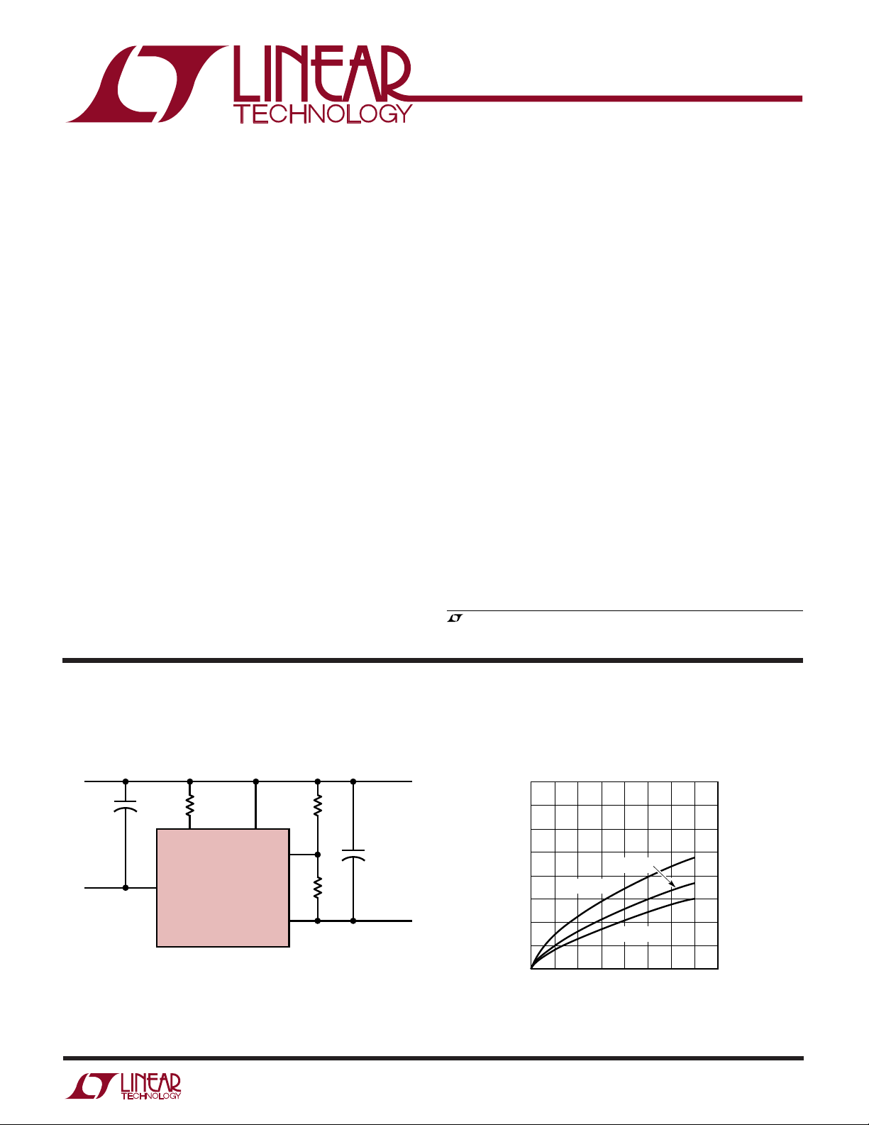
5V, 3A Regulator with 3.5A Current Limit
C2
2µF
TANT
R
*
LIM
4.3k
REF GND
V
LT1185
IN
= 3.5A
LIM
R1
2.37k
+
FB
R2
2.67k
V
OUT
C1
2µF
TANT
5V AT 3A
LT1185 • TA01
Dropout Voltage
+
V
OUT
–
(V)
OUT
–V
IN
V
1.6
1.4
1.2
1.0
0.8
0.6
0.4
0.2
TJ = 25°C
TJ = 125°C
TJ = –55°C
0
0
1
2
LOAD CURRENT (A)
3
LT1185 • TA02
4
1
Page 2
LT1185
A
W
O
LUTEXI TIS
S
A
WUW
U
ARB
G
(Note 1)
Input Voltage .......................................................... 35V
Input-Output Differential ......................................... 30V
FB Voltage ................................................................ 7V
REF Voltage .............................................................. 7V
Output Voltage........................................................ 30V
Output Reverse Voltage ............................................ 2V
Operating Ambient Temperature Range
LT1185C ............................................... 0°C to 70°C
LT1185M ......................................... –55°C to 125°C
Operating Junction Temperature Range*
Control Section
LT1185C ............................................. 0°C to 125°C
LT1185I .......................................... –40°C to 125°C
LT1185M ........................................ –55°C to 150°C
Power Transistor Section
LT1185C ............................................. 0°C to 150°C
LT1185I .......................................... –40°C to 150°C
LT1185M ........................................ –55°C to 175°C
Storage Temperature Range ................ – 65°C to 150°C
Lead Temperature (Soldering, 10 sec)................ 300°C
*See Application Section for details on calculating Operation Junction Temperature
/
PACKAGE
GND FB
V
OUT
4-LEAD TO-3 METAL CAN
θ
TAB IS V
IN
θ
O
RDER I FOR ATIO
BOTTOM VIEW
1
4
K PACKAGE
JC MAX
5-LEAD PLASTIC TO-220
JC MAX
2
3
= 2.5°C/W, θJA = 35°C/W
FRONT VIEW
5
4
3
2
1
T PACKAGE
= 2.5°C/W, θJA = 50°C/W
REF
V
IN
(CASE)
REF
V
OUT
V
IN
FB
GND
WU
U
ORDER PART
NUMBER
LT1185MK
ORDER PART
NUMBER
LT1185CT
LT1185IT
ELECTRICAL CHARACTERISTICS
The ● denotes specifications which apply over the operating temperature range, otherwise specifications are at TA = 25°C.
Adjustable version, VIN = 7.4V, V
PARAMETER CONDITIONS MIN TYP MAX UNITS
Reference Voltage (At FB Pin) 2.37 V
Reference Voltage Tolerance (At FB Pin) (Note 2) VIN – V
Feedback Pin Bias Current V
Droput Voltage (Note 3) I
Load Regulation (Note 7) I
Line Regulation (Note 7) VIN – V
Minimum Input Voltage I
Internal Current Limit (See Graph for 1.5V ≤ VIN – V
Guaranteed Curve) (Note 12)
OUT
= 5V, I
= 1mA, R
OUT
OUT
1mA ≤ I
OUT
V
– V
IN
OUT
P ≤ 25W (Note 6), V
≤ TJ ≤ T
T
MIN
= V
OUT
= 0.5A, V
OUT
= 3A, V
I
OUT
= 5mA to 3A 0.05 0.3 %
OUT
V
– V
IN
OUT
OUT
= 1A (Note 4), V
OUT
I
= 3A 4.3 V
OUT
– V
V
IN
OUT
V
– V
IN
OUT
– V
V
IN
OUT
= 4.02k, unless otherwise noted.
LIM
= 5V, V
≤ 3A ● 1 ±2.5 %
= 1.2V to VIN = 30V
REF
OUT
= 1.5V to 10V, V
= 1V to 20V, V
= 15V ● 2.0 3.0 4.2 A
= 20V ● 1.0 1.7 2.6 A
= 30V ● 0.2 0.4 1.0 A
= V
OUT
REF
= 5V
OUT
(Note 9)
MAX
● 0.7 2 µA
= 5V 0.20 0.37 V
OUT
= 5V 0.67 1.00 V
= 5V
OUT
= 5V 0.002 0.01 %/V
OUT
= V
OUT
REF
≤ 10V 3.3 3.6 4.2 A
OUT
● 3.1 4.4 A
0.3 ±1%
4.0 V
2
Page 3
LT1185
ELECTRICAL CHARACTERISTICS
The ● denotes specifications which apply over the operating temperature range, otherwise specifications are at TA = 25°C.
Adjustable version, VIN = 7.4V, V
PARAMETER CONDITIONS MIN TYP MAX UNITS
External Current Limit 5k ≤ R
Programming Constant (Note 11)
External Current Limit Error 1A ≤ I
Quiescent Supply Current I
Supply Current Change with Load VIN – V
REF Pin Shutoff Current ● 0.4 2 7 µA
Thermal Regulation (See Applications VIN – V
Information) I
Reference Voltage Temperature Coefficient (Note 8) 0.003 0.01 %/°C
Thermal Resistance Junction to Case TO-3 Control Area 1 °C/W
OUT
= 5V, I
= 1mA, R
OUT
R
LIM
OUT
4V ≤ V
V
– V
IN
OUT
LIM
LIM
= 15k • A/I
= 5mA, V
IN
OUT
OUT
OUT
= 5mA to 2A
= 4.02k, unless otherwise noted.
LIM
≤ 15k, V
≤ 3A 0.02 I
= 1V ● 15k A•Ω
OUT
0.06 I
OUT
LIM
= V
REF
● 0.04 I
● 2.5 3.5 mA
LIM
LIM
0.09 I
LIM
LIM
+ 0.03 A
+ 0.05 A
≤ 25V (Note 5)
= V
(Note 10) ● 25 40 mA/A
SAT
≥ 2V ● 10 25 mA/A
= 10V 0.005 0.014 %/W
Power Transistor 3 °C/W
TO-220 Control Area 1 °C/W
Power Transistor 3 °C/W
Note 1: Absolute Maximum Ratings are those values beyond which the life
of a device may be impaired.
Note 2: Reference voltage is guaranteed both at nominal conditions (no
load, 25°C) and at worst-case conditions of load, line, power and
temperature. An intermediate value can be calculated by adding the effects
of these variables in the actual application. See the Applications
Information section of this data sheet.
Note 3: Dropout voltage is tested by reducing input voltage until the
output drops 1% below its nominal value. Tests are done at 0.5A and 3A.
The power transistor looks basically like a pure resistance in this range so
that minimum differential at any intermediate current can be calculated by
interpolation; V
= 0.25V + 0.25Ω • I
DROPOUT
. For load current less than
OUT
0.5A, see graph.
Note 4: “Minimum input voltage” is limited by base emitter voltage drive
of the power transistor section, not saturation as measured in Note 3. For
output voltages below 4V, “minimum input voltage” specification may limit
dropout voltage before transistor saturation limitation.
Note 5: Supply current is measured on the ground pin, and does not
include load current, R
, or output divider current.
LIM
Note 6: The 25W power level is guaranteed for an input-output voltage of
8.3V to 17V. At lower voltages the 3A limit applies, and at higher voltages
the internal power limiting may restrict regulator power below 25W. See
graphs.
Note 7: Line and load regulation are measured on a pulse basis with a
pulse width of ≈2ms, to minimize heating. DC regulation will be affected
by thermal regulation and temperature coefficient of the reference. See
Applications Information section for details.
Note 8: Guaranteed by design and correlation to other tests, but not
tested.
Note 9: T
= 0°C for the LT1185C, –40°C for LT1185I, and –55°C for
JMIN
the LT1185M. Power transistor area and control circuit area have different
maximum junction temperatures. Control area limits are T
= 125°C for
JMAX
the LT1185C and LT1185I and 150°C for the LT1185M. Power area limits
are 150°C for LT1185C and LT1185I and 175°C for LT1185M.
Note 10: V
0.25V + 0.25 • I
is the maximum specified dropout voltage;
SAT
.
OUT
Note 11: Current limit is programmed with a resistor from REF pin to GND
pin. The value is 15k/I
Note 12: For V
IN
.
LIM
– V
= 1.5V; VIN = 5V, V
OUT
= 3.5V. V
OUT
= 1V for all
OUT
other current limit tests.
3
Page 4
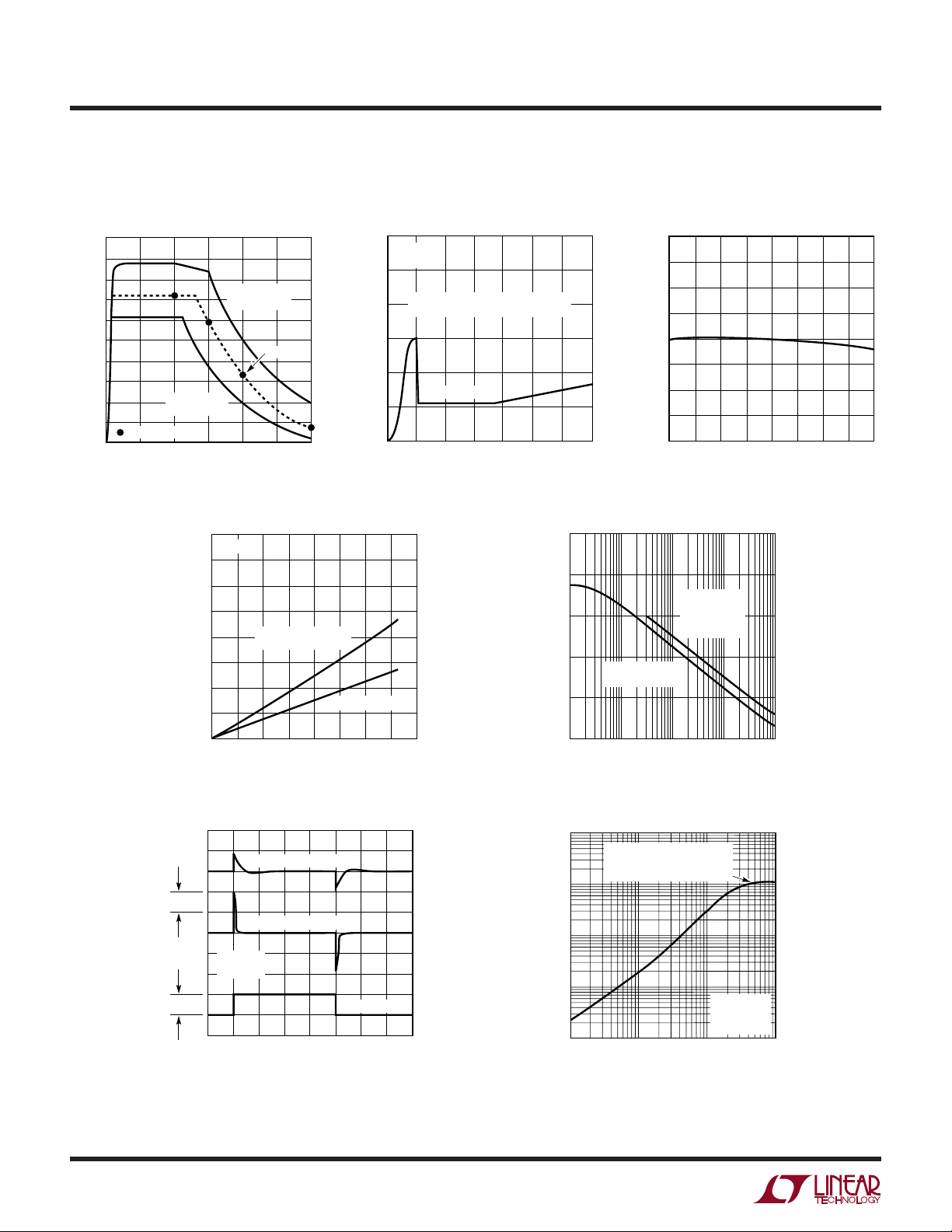
LT1185
LPER
Internal Current Limit
5
4
3
2
OUTPUT CURRNT (A)
1
TEST POINTS
0
0
5
INPUT-OUTPUT DIFFERENTIAL (V)
F
GUARANTEED
LIMIT
15 20
10
R
O
GUARANTEED
LIMIT
TYPICAL
ATYPICA
25
LT1185 • TPC01
UW
CCHARA TERIST
E
C
Quiescent Ground Pin Current*
12
I
LOAD
= 25°C
T
J
10
*DOES NOT INCLUDE REF CURRENT
8
OR OUTPUT DIVIDER CURRENT
6
4
GROUND PIN CURRENT (mA)
2
0
0
30
510
= 0
V
= 5V
OUT
15 25
INPUT VOLTAGE (V)
ICS
20 30 35
LT1185 • TPC02
Feedback Pin Voltage
Temperature Drift
2.41
2.40
2.39
2.38
2.37
VOLTAGE (V)
2.36
2.35
2.34
2.33
–50
–25
0
JUNCTION TEMPERATURE (°C)
75
50
25
100
125
LT1185 • TPC03
150
Ground Pin Current
160
TJ = 25°C
140
120
100
0
REGULATOR JUST AT
DROPOUT POINT
1
LOAD CURRENT (A)
80
60
CURRENT (mA)
40
20
0
Load Transient Response
C
= 2.2µF, ESR = 1Ω
OUT
100mV
C
= 2.2µF, ESR = 2Ω
OUT
V
= 5V
OUT
= 1A
I
OUT
∆I
LOAD
0
26
4
2
8
TIME (µs)
VIN – V
10
= 5V
OUT
3
LT1185 • TPC04
0.1A tr,f ≤ 100ns
14
12
LT1185 • TPC06
Ripple Rejection vs Frequency
–100
–80
V
OUT
OUT
= 1.5V
ALL OUTPUT
VOLTAGES
WITH 0.05µF
ACROSS R2
= 5V
LT1185 • TPC05
(dB)
–60
IN
/V
OUT
–40
RATIO V
–20
0
4
100 10k 100k 1M
– V
V
IN
1k
FREQUENCY (Hz)
Output Impedance
10
1
0.1
IMPEDANCE (Ω)
0.01
16
0.001
1k
OUTPUT IMPEDANCE IS
SET BY OUTPUT CAPACITOR
ESR IN THIS REGION
V
OUT
I
OUT
C
OUT
FREQUENCY (Hz)
= 5V
= 1A
= 2.2µF
LT1183 • TPC07
1M10k 100k
4
Page 5
UU W U
APPLICATIO S I FOR ATIO
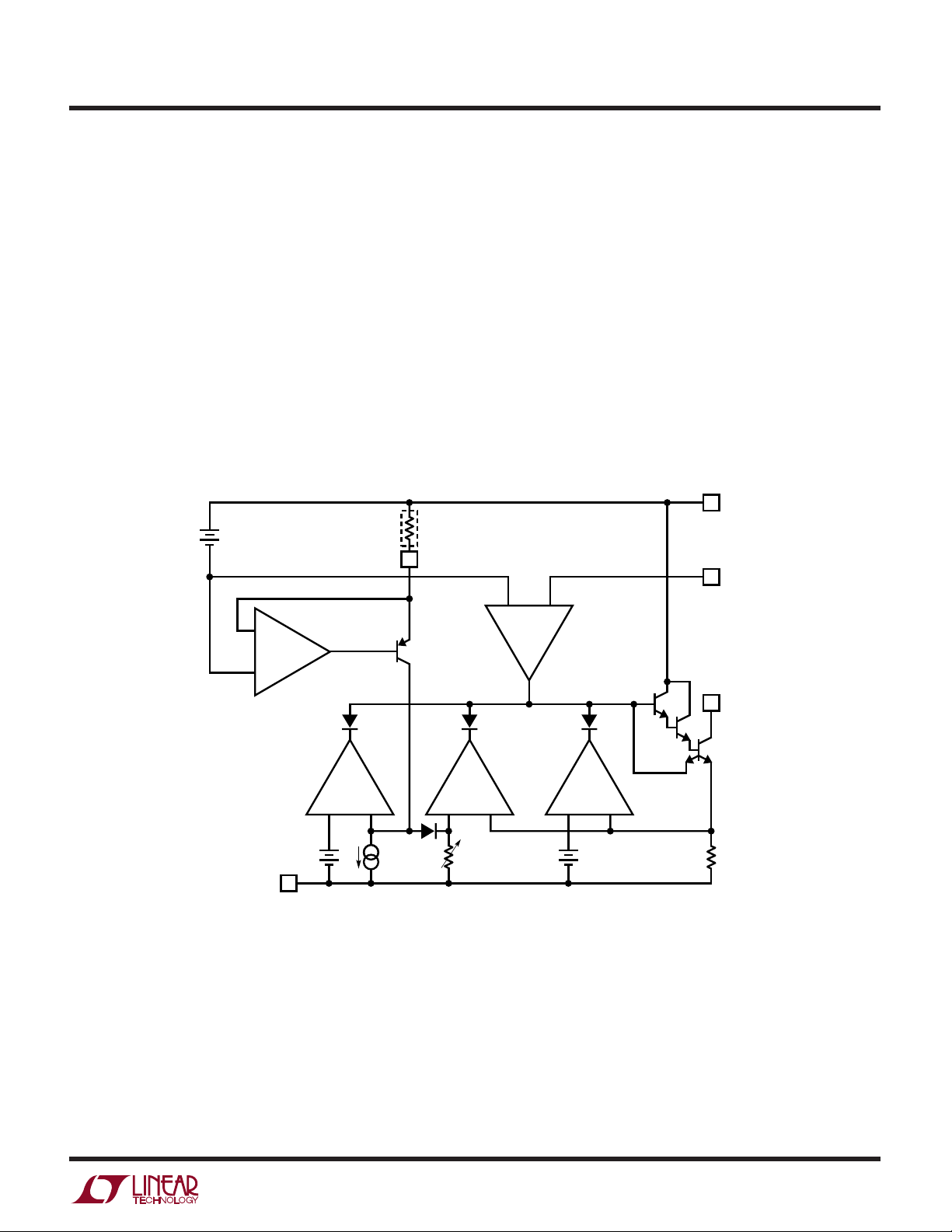
Block Diagram
LT1185
A simplified block diagram of the LT1185 is shown in
Figure 1. A 2.37V bandgap reference is used to bias the
input of the error amplifier A1, and the reference amplifier
A2. A1 feeds a triple NPN pass transistor stage which has
the two driver collectors tied to ground so that the main
pass transistor can completely saturate. This topology
normally has a problem with unlimited current in Q1 and
Q2 when the input voltage is less than the minimum
required to create a regulated output. The standard “fix”
for this problem is to insert a resistor in series with Q1 and
Q2 collectors, but this resistor must be low enough in
value to supply full base current for Q3 under worst-case
(EXTERNAL)
V
REF
2.37V
–
A2
+
R
LIM
REF
Q4
conditions, resulting in very high supply current when the
input voltage is low. To avoid this situation, the LT1185
uses an auxiliary emitter on Q3 to create a drive limiting
feedback loop which automatically adjusts the drive to Q1
so that the base drive to Q3 is just enough to saturate Q3,
but no more. Under saturation conditions, the auxiliary
emitter is acting like a collector to shunt away the output
current of A1. When the input voltage is high enough to
keep Q3 out of saturation, the auxiliary emitter current
drops to zero even when Q3 is conducting full load current.
GND
FB
+
–
A1
Q2
LT1185 • BD
Q3
R2
0.055Ω
V
OUT
Q1
D2 D4 D3
A5
+
–
300mV
V
IN
I1
2µA
A4
+
–
D1
R1
350Ω
+
A3
–
200mV
Figure 1. Block Diagram
5
Page 6

LT1185
UU W U
APPLICATIO S I FOR ATIO
Amplifier A2 is used to generate an internal current through
Q4 when an external resistor is connected from the REF
pin to ground. This current is equal to 2.37V divided by
R
. It generates a current limit sense voltage across R1.
LIM
The regulator will current limit via A4 when the voltage
across R2 is equal to the voltage across R1. These two
resistors essentially form a current “amplifier” with a gain
of 350/0.055 = 6,360. Good temperature drift is inherent
because R1 and R2 are made from the same diffusions.
Their ratio, not absolute value, determines current limit.
Initial accuracy is enhanced by trimming R1 slightly at
wafer level. Current limit is equal to 15kΩ/R
LIM
.
D1 and I1 are used to guarantee regulator shutdown when
REF pin current drops below 2µA. A current less than 2µA
through Q4 causes the +input of A5 to go low and shut
down the regulator via D2.
A3 is an internal current limit amplifier which can override
the external current limit. It provides “goof proof” protection for the pass transistor. Although not shown, A3 has
a nonlinear foldback characteristic at input-output voltages above 12V to guarantee safe area protection for Q3.
See the graph, Internal Current Limit in the Typical Performance Characteristics of this data sheet.
Setting Output Voltage
The LT1185 output voltage is set by two external resistors
(see Figure 2). Internal reference voltage is trimmed to
2.37V so that a standard 1% 2.37k resistor (R1) can be
used to set divider current at 1mA. R2 is then selected
from:
(V
– 2.37) R1
R2 =
for R1 = 2.37k and V
R2 = V
OUT
OUT
V
REF
– 2.37k
= 2.37V, this reduces to:
REF
suggested values of 1% resistors are shown.
V
OUT
5V 2.67k
5.2V 2.87k
6V 3.65k
12V 9.76k
15V 12.7k
R2 WHEN R1 = 2.37k
Output Capacitor
The LT1185 has a collector output NPN pass transistor,
which makes the open-loop output impedance much
higher than an emitter follower. Open-loop gain is a direct
function of load impedance, and causes a main-loop
“pole” to be created by the output capacitor, in addition to
an internal pole in the error amplifier. To ensure loop
stability, the output capacitor must have an ESR (effective
series resistance) which has an upper limit of 2Ω, and a
lower limit of 0.2 divided by the capacitance in µF. A 2µF
output capacitor, for instance, should have a maximum
ESR of 2Ω, and a minimum of 0.2/2 = 0.1Ω. These values
are easily encompassed by standard solid tantalum
capacitors, but occasionally a solid tantalum unit will have
abnormally high ESR, especially at very low temperatures. The suggested 2µF value shown in the circuit
applications should be increased to 4.7µF for –40°C and
–55°C designs if the 2µF units cannot be guaranteed to
stay below 2Ω at these temperatures.
Although solid tantalum capacitors are suggested, other
types can be used if they meet the ESR requirements.
Standard aluminum electrolytic capacitors need to be
upward of 25µF in general to hold 2Ω maximum ESR,
especially at low temperatures. Ceramic, plastic film, and
monolithic capacitors have a problem with ESR being too
low
. These types should have a 1Ω carbon resistor in
series to guarantee loop stability.
The output capacitor should be located close to the regu-
lator (≤3") to avoid excessive impedance due to lead
inductance. A six inch lead length (2 • 3") will generate an
extra 0.8Ω inductive reactance at 1MHz, and unity-gain
frequency can be up to that value.
For remote sense applications, the capacitor should still be
located close to the regulator. Additional capacitance can
be added at the remote sense point, but the remote
capacitor must be at least 2µF solid tantalum. It cannot be
a low ESR type like ceramic or mylar unless a 0.5Ω to 1Ω
carbon resistor is added in series with the capacitor. Logic
boards with multiple low ESR bypass capacitors should
have a solid tantalum unit added in parallel whose value is
approximately five times the combined value of low ESR
capacitors.
6
Page 7

UU W U
APPLICATIO S I FOR ATIO
LT1185
Large output capacitors (electrolytic or solid tantalum)
will not cause the LT1185 to oscillate, but they will cause
a damped “ringing” at light load currents where the ESR
of the capacitor is several orders of magnitude lower than
the load resistance. This ringing only occurs as a result of
transient load or line conditions and normally causes no
problems because of its low amplitude (≤25mV).
Heat Sinking
The LT1185 will normally be used with a heat sink. The size
of the heat sink is determined by load current, input and
output voltage, ambient temperature, and the thermal
resistance of the regulator, junction-to-case (θJC). The
LT1185 has two separate values for θJC: one for the power
transistor section, and a second, lower value for the
control section. The reason for two values is that the
power transistor is capable of operating at higher continuous temperature than the control circuitry. At low power
levels, the two areas are at nearly the same temperature,
and maximum temperature is limited by the control area.
At high power levels, the power transistor will be at a
significantly higher temperature than the control area
and its maximum operating temperature will be the
limiting factor.
To calculate heat sink requirements, you must solve a
thermal resistance formula twice, one for the power
transistor and one for the control area. The
obtained for heat sink thermal resistance must be used. In
these equations, two values for maximum junction temperature and junction-to-case thermal resistance are used,
as given in Electrical Specifications.
lowest
value
Example: A commercial version of the LT1185 in the
TO-220 package is to be used with a maximum ambient
temperature of 60°C. Output voltage is 5V at 2A. Input
voltage can vary from 6V to 10V. Assume an interface
resistance of 1°C/W.
First solve for control area, where the maximum junction
temperature is 125°C for the TO-220 package, and
θJC = 1°C/W:
P = (10V – 5V) (2A) +
2A
(10V) = 10.5W
40
125°C – 60°C
θ
HS =
Next, solve for power transistor limitation, with
T
= 150°C, θJC = 3°C/W:
JMAX
θHS =
The lowest number must be used, so heat sink resistance
must be less than 4.2°C/W.
Some heat sink data sheets show graphs of heat sink
temperature rise vs power dissipation instead of listing a
value for thermal resistance. The formula for θHS can be
rearranged to solve for maximum heat sink temperature
rise:
∆THS = T
Using numbers from the previous example:
10.5W
150 – 60
10.5
– T
JMAX
– 1°C/W – 1°C/W = 4.2°C/W
– 3 – 1 = 4.6°C/W
– P(θJC + θ
AMAX
CHS
)
(T
θHS =
θ
= Maximum heat sink thermal resistance
HS
= LT1185 junction-to-case thermal resistance
θ
JC
= Case-to-heat sink (interface) thermal
θ
CHS
resistance, including any insulating washers
= LT1185 maximum operating junction
T
JMAX
temperature
= Maximum ambient temperature in
T
AMAX
customers application
P = Device dissipaton
= (V
JMAX
– V
IN
– T
P
OUT
AMAX
) (I
)
– θJC – θ
) +
OUT
I
OUT
40
CHS
(VIN)
.
∆THS = 125°C – 60 – 10.5(1 + 1) = 44°C control
section
∆THS = 150°C – 60 – 10.5(3 + 1) = 48°C power
transistor
The smallest rise must be used, so heat sink temperature
rise must be less than 44°C at a power level of 10.5W.
For board level applications, where heat sink size may be
critical, one is often tempted to use a heat sink which
barely meets the requirements. This is permissible
correct assumptions were made concerning maximum
ambient temperature and power levels. One complicating
if
7
Page 8

LT1185
UU W U
APPLICATIO S I FOR ATIO
factor is that local ambient temperature may be somewhat
higher because of the point source of heat. The consequences of excess junction temperature include poor
reliability, especially for plastic packages, and the possibility of thermal shutdown or degraded electrical characteristics. The final design should be checked
thermocouple attached to the regulator case under worstcase conditions of high ambient, high input voltage and
full load.
What About Overloads?
IC regulators with thermal shutdown, like the LT1185,
allow heat sink designs which concentrate on worst-case
“normal” conditions and ignore “fault” conditions. An
output overload or short may force the regulator to exceed
its maximum junction temperature rating, but thermal
shutdown is designed to prevent regulator failure under
these conditions. A word of caution however; thermal
shutdown temperatures are typically 175°C in the control
portion of the die and 180°C to 225°C in the power
transistor section. Extended operation at these temperatures can cause permanent degradation of plastic encapsulation. Designs which may be subjected to extended
periods of overload should either use the hermetic TO-3
package or increase heat sink size. Foldback current
limiting can be implemented to minimize power levels
under fault conditions.
External Current Limit
The LT1185 requires a resistor to set current limit. The
value of this resistor is 15k divided by the desired current
limit (in amps). The resistor for 2A current limit would be
15k/2A = 7.5k. Tolerance over temperature is ±10%, so
current limit is normally set 15% above maximum load
current. Foldback limiting can be employed if short-circuit
current must be lower than full load current (see Typical
Applications).
The LT1185 has internal current limiting which will override external current limit if power in the pass transistor is
in situ
with a
excessive. The internal limit is ≈3.6A with a foldback
characteristic which is dependent on input-output voltage,
not output voltage
teristics).
Ground Pin Current
Ground pin current for the LT1185 is approximately 2mA
plus I
2mA + 3/40 = 77mA. Worst case guarantees on the ratio of
I
OUT
Specifications.
Ground pin current can be important for two reasons. It
adds to power dissipation in the regulator and it can affect
load/line regulation if a long line is run from the ground pin
to load ground. The additional power dissipation is found
by multiplying ground pin current by input voltage. In a
typical example, with VIN = 8V, V
LT1185 will dissipate (8V – 5V)(2A) = 6W in the pass
transistor and (2A/40)(8V) = 0.4W in the internal drive
circuitry. This is only a 1.5% efficiency loss, and a 6.7%
increase in regulator power dissipation, but these values
will increase at higher output voltages.
Ground pin current can affect regulation as shown in
Figure 2. Parasitic resistance in the ground pin lead will
create a voltage drop which
load current is increased. Similarly, output voltage can
decrease
component of ground pin current drops significantly at
higher input-output differentials. These effects are small
enough to be ignored for local regulation applications, but
for remote sense applications, they may need to be considered. Ground lead resistance of 0.4Ω would cause an
output voltage error of up to (3A/40)(0.4Ω) = 30mV, or
0.6% at V
connected as shown in Figure 2, with ra ≈ 0Ω, this error is
a fixed number of millivolts, and does not increase as a
function of DC output voltage.
/40. At I
OUT
to ground pin current are contained in the Electrical
as input voltage increases because the “I
OUT
per se
(see Typical Performace Charac-
= 3A, ground pin current is typically
OUT
= 5V and I
OUT
increases
= 5V. Note that if the sense leads are
output voltage as
= 2A, the
OUT
OUT
/40”
8
Page 9

UU W U
APPLICATIO S I FOR ATIO
+
R
V
IN
–
LIM
REF GND
V
LT1185
IN
PARASITIC
LEAD RESISTANCES
r
a
FB
– r
R1*
2.37k
R2
I
GND
LT1185
+
+
b
LOAD
V
OUT
V
OUT
*R1 SHOULD BE CONNECTED DIRECTLY TO GROUND LEAD, NOT TO THE LOAD,
SO THAT r
ERRORS CREATED BY r
INCREASES
DIRECTLY TO LOAD FOR REMOTE SENSING
≈ 0Ω. THIS LIMITS THE OUTPUT VOLTAGE ERROR TO (I
a
WITH INCREASING GROUND PIN CURRENT. R2 SHOULD BE CONNECTED
ARE MULTIPLIED BY (1 + R2/R1). NOTE THAT V
a
Figure 2. Proper Connection of Positive Sense Lead
Shutdown Techniques
The LT1185 can be shut down by open-circuiting the REF
pin. The current flowing into this pin must be less than
0.4µA to guarantee shutdown. Figure 3 details several
ways to create the “open” condition, with various logic
levels. For variations on these schemes, simply remember
that the voltage on the REF pin is 2.4V negative with
respect to the ground pin.
Output Overshoot
Very high input voltage slew rate during start-up may
cause the LT1185 output to overshoot. Up to 20% overshoot could occur with input voltage ramp-up rate exceeding 1V/µs. This condition cannot occur with normal 50Hz
to 400Hz rectified AC inputs because parasitic resistance
and inductance will limit rate of rise even if the power
switch is closed at the peak of the AC line voltage. This
assumes that the switch is in the AC portion of the circuit.
–
LT1185 • F02
)(rb).
GND
OUT
If instead, a switch is placed directly in the regulator input
so that a large filter capacitor is precharged, fast input slew
rates will occur on switch closure. The output of the
regulator will slew at a rate set by current limit and output
capacitor size; dVdt = I
LIM/COUT
. With I
= 3.6A and C
LIM
OUT
= 2.2µF, the output will slew at 1.6V/µs and overshoot can
occur. This overshoot can be reduced to a few hundred
millivolts or less by increasing the output capacitor to
10µF and/or reducing current limit so that output slew rate
is held below 0.5V/µs.
A second possibility for creating output overshoot is
recovery from an output short. Again, the output slews at
a rate set by current limit and output capacitance. To avoid
overshoot, the ratio I
LIM/COUT
should be less than
0.5 × 10⁶. Remember that load capacitance can be added
to C
supply bypass capacitors that total more than C
for this calculation. Many loads will have multiple
OUT
OUT
.
9
Page 10

LT1185
UU W U
APPLICATIO S I FOR ATIO
5V Logic, Positive Regulated Output
+
†
R
LIM
4k
REF GND
FB
V
IN
R6
R7
†
30k
2.4k
–
LT1185
V
IN
*CMOS LOGIC
†
FOR HIGHER VALUES OF R
V
OUT
R1
R2
LIM
+
V
+
LT1185 • F3a
, MAKE R7 = (R
OUT
R5
300k
LIM
5V
*
Q1
2N3906
)(0.6)
5V Logic, Negative Regulated Output
5V
“HI” = OUTPUT “OFF”
3 EA 1N4148
Q1
2N3906
R4
33k
V
IN
–
R
LIM
REF GND
LT1185V
IN
FB
V
OUT
LT1185 • F03b
Figure 3. Shutdown Techniques
10
Page 11

UU W U
APPLICATIO S I FOR ATIO
LT1185
Thermal Regulation
IC regulators have a regulation term not found in discrete
designs because the power transistor is thermally coupled
to the reference. This creates a shift in the output voltage
which is proportional to power dissipation in the regulator.
∆V
K1 and K2 are constants. K1 is a fast time constant effect
caused by die temperature
lished within 50ms of a power change. K1 is specified on
the data sheet as thermal regulation, in percent per watt.
K2 is a long time constant term caused by the temperature
drift of the regulator reference voltage. It is also specified,
but in percent per degree centigrade. It must be multiplied
by overall thermal resistance, junction-to-ambient, θJA.
As an example, assume a 5V regulator with an input
voltage of 8V, load current of 2A, and a total thermal
resistance of 4°C/W, including junction-to-case, (use
control area specification), interface, and heat sink resistance. K1 and K2, respectively, from the data sheet are
0.014%/W and 0.01%/°C.
= P(K1 + K2 θJA)
OUT
= (I
)(VIN – V
OUT
)(K1 + K2 θJA)
OUT
gradients
which are estab-
This shift in output voltage could be in either direction
because K1 and K2 can be either positive or negative.
Thermal regulation is already included in the worst case
reference specification.
Output Voltage Reversal
Some IC regulators suffer from a latch-up state when their
output is forced to a reverse voltage of as little as one diode
drop. The latch-up state can be triggered without a fault
condition when the load is connected to an opposite
polarity supply instead of to ground. If the second supply
is turned on first, it will pull the output of the first supply
to a reverse voltage through the load. The first supply may
then latch off when turned on. This problem is particularly
annoying because the diode clamps which should always
be used to protect against polarity reversal do not usually
stop the latch-up problem.
The LT1185 is designed to allow output reverse polarity of
several volts without damage or latch-up, so that a simple
diode clamp can be used.
∆V
= (2A)(8V –␣ 5V)(0.014 + 0.01 • 4)
OUT
= 0.32%
11
Page 12

LT1185
U
TYPICAL APPLICATIO S
Foldback Current Limiting
+
R4
R3
15k
+
V
IN
–
2µF
TANT
LT1185V
IN
2N3906
REFGND
V
OUT
LT1185 • TA03a
Q1
FB
5.36k
R1
2.37k
R2
2.61k
+
2µF
TANT
+
V
OUT
–
1.6
1.4
1.2
1.0
0.8
(NORMALIZED)
0.6
OUT
V
0.4
0.2
0
FULL LOAD
I
SHORT-CIRCUIT
I
OUT
10.8k
15k
+I
=
R4
R3
15k
=
R3
LT1185 • TA03b
Auxiliary + 12V Low Dropout Regulator for Switching Supply
*
R
LIM
+
REF GND
FB
R1
2.37k
12V
REGULATED
AUXILIARY
+
12
V
PRIMARY
*
+
*DIODE CONNECTION INDICATES A FLYBACK
SWITCHING TOPOLOGY, BUT FORWARD
CONVERTERS MAY ALSO BE USED
LT1185
IN
V
OUT
5V
CONTROL
R2
9.76k
5V
MAIN
OUTPUT
LT1185 • TA04
Page 13

U
INPUT VOLTAGE (V)
0
TIME CONSTANTS (t)*
1.5
2.0
2.5
15
25
LT1185 • TA07
1.0
0.5
0
510 20
3.0
3.5
4.0
30
*t = (R3//R
LIM
)(C3) =
()
R3 • R
LIM
R3 + R
LIM
(C3)
TYPICAL APPLICATIO S
Low Input Voltage Monitor Tracks Dropout Characteristics
LT1185
C1
2.2µF
TANT
+
V
OUT
*3" #26 WIRE
**R4 DETERMINES TRIP POINT AT I
R6 DETERMINES INCREASE OF TRIP POINT AS I
TRIP POINT FOR V
FOR VALUES SHOWN, TRIP POINT FOR VIN IS:
+ 0.37V AT I
V
OUT
†
DO NOT SUBSTITUTE. OP AMP MUST HAVE COMMON MODE
RANGE EQUAL TO NEGATIVE SUPPLY
= V
IN
OUT
= 0 AND V
OUT
= 0
OUT
R4 • R7
1 +
()
R3 • R6
= 1.18V AT I
OUT
+ I
OUT
OUT
INCREASES
R5 • R7
R6
OUT
= 3A
–
+
–
TO V
IN
IN
+
C2
+
2.2µF
V
IN
TANT
0.01Ω
R5*
–
R6**
R3
360k
R4**
1k
1k
4k
REF GND
LT1185V
IN
R7
27k
OPTIONAL HYSTERSIS
≈2M
3
+
†
LT1006
2
–
V
–
4
+
V
V
7
LT1185 • TA05
FB
OUT
R1
2.37k
+
R2
2.6k
“LOW” FOR LOW INPUT
OUTPUT SWINGS FROM V
+
V
IN
+
–
ALL DIODES 1N4148
*SEE CHART FOR DELAY TIME VERSUS (C3)(R3//R
**FOR LONG DELAY TIMES, REPLACE D2 WITH 2N3906 TRANSISTOR AND USE R3 ONLY FOR
CALCULATING DELAY TIME. R3 CAN INCREASE TO 100k
***I
COEFFICIENT OF I
FOR COLD OPERATION
†
Time Delayed Start-Up
R3**
†
D3
15k
D2
Q1**
C2
2.2µF
IS ≈11k/R
LIM
D3 PROVIDES FAST RESET OF TIMING. INPUT MUST DROP TO A LOW VALUE TO RESET TIMING
C3*
, INSTEAD OF 15k, BECAUSE OF VOLTAGE DROP IN D1. TEMPERATURE
LIM
WILL BE ≈0.11%/°C, SO ADEQUATE MARGIN MUST BE ALLOWED
LIM
R
***
LIM
D1
REF GND
LT1185V
IN
LIM
V
) PRODUCT
FB
OUT
R1
2.37k
R2
C1
+
2.2µF
TANT
LT1185 • TA06
V
Delay Time
+
OUT
–
13
Page 14
LT1185
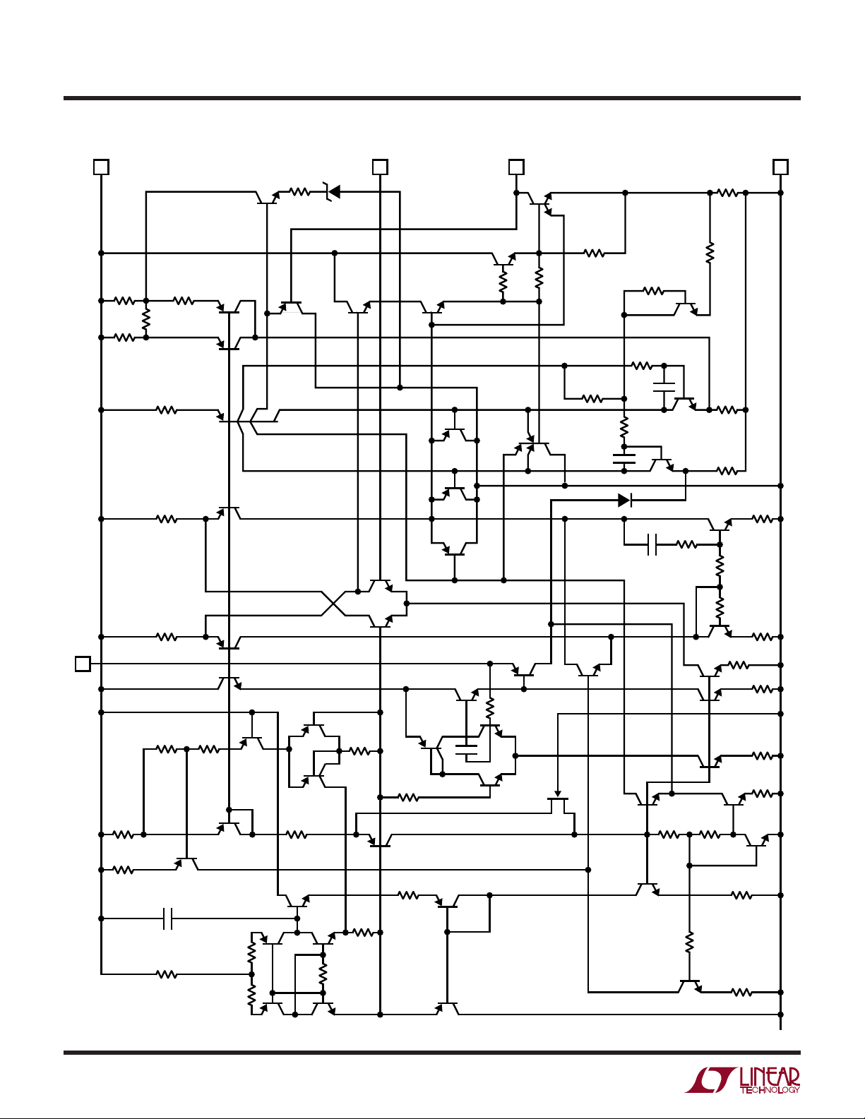
WW
SCHE ATIC DIAGRA
GND
R16
R17
R15
0.055Ω
1k
400Ω
R43
50k
R39
IN
V
LT1185 • SD
1k
R23
OUT
V
Q24
R26
R34
1k
R38
20k
R36
20k
300Ω
C5
10pF
20k
R35
C4
10pF
Q27
D1
C3
30pF
Q23
6k
R24
80Ω
Q28
R31
Q25
Q26
R44
R28
200Ω
R37
R38
Q32
5k
FB
D4
R19
20k
Q20
1k
6k
4k
R14
R13
R18
3.2k
2k
2k
Q19
Q18
Q17
Q16
Q53
Q21
Q22
Q29Q30Q31
REF
Q14Q13
R12
2k
R7
500Ω
R6
750Ω
500Ω
C1
10pF
R1
5.5k
Q15
Q42
Q46
C2
Q49 Q47
Q45
Q43
R52
Q44
10k
Q52
Q9
R8
6.5k
Q8
R9
Q7
Q6
3k
R3
3k
R2
2.7k
Q5
Q2
R4
520Ω
Q1
Q12
Q11
R11
220Ω
R53
10k
Q48
R54
4k
R5
Q4
Q3
600Ω
Q41
Q51
Q39
R49
R55
Q35
Q36
700Ω
30k
Q50
R50
Q34
160Ω
Q33
R42
R45
Q40
R56
50k
1.3k
10k
R40
1k
R48
2k
R47
4k
R46
8k
Q37
600Ω
14
Page 15

PACKAGE DESCRIPTIO
0.320 – 0.350
(8.13 – 8.89)
0.420 – 0.480
(10.67 – 12.19)
0.760 – 0.775
(19.30 – 19.69)
U
Dimensions in inches (millimeters) unless otherwise noted.
K Package
4-Lead TO-3 Metal Can
(LTC DWG # 05-08-1311)
1.177 – 1.197
(29.90 – 30.40)
0.060 – 0.135
(1.524 – 3.429)
0.038 – 0.043
(0.965 – 1.09)
18°
0.470 TP
P.C.D.
72°
LT1185
0.655 – 0.675
(16.64 – 19.05)
0.151 – 0.161
(3.84 – 4.09)
DIA 2 PLC
0.167 – 0.177
(4.24 – 4.49)
R
0.495 – 0.525
(12.57 – 13.34)
R
K4(TO-3) 0695
0.390 – 0.415
(9.906 – 10.541)
0.460 – 0.500
(11.684 – 12.700)
0.057 – 0.077
(1.448 – 1.956)
0.147 – 0.155
(3.734 – 3.937)
0.230 – 0.270
(5.842 – 6.858)
0.330 – 0.370
(8.382 – 9.398)
0.028 – 0.038
(0.711 – 0.965)
T Package
5-Lead Plastic TO-220 (Standard)
(LTC DWG # 05-08-1421)
DIA
0.570 – 0.620
(14.478 – 15.748)
0.152 – 0.202
0.260 – 0.320
(6.60 – 8.13)
(3.861 – 5.131)
0.165 – 0.180
(4.191 – 4.572)
0.700 – 0.728
(17.78 – 18.491)
0.135 – 0.165
(3.429 – 4.191)
0.045 – 0.055
(1.143 – 1.397)
0.620
(15.75)
TYP
0.095 – 0.115
(2.413 – 2.921)
0.013 – 0.023
(0.330 – 0.584)
0.155 – 0.195
(3.937 – 4.953)
T5 (TO-220) 0398
Information furnished by Linear Technology Corporation is believed to be accurate and reliable.
However, no responsibility is assumed for its use. Linear Technology Corporation makes no representation that the interconnection of circuits as described herein will not infringe on existing patent rights.
15
Page 16

LT1185
U
TYPICAL APPLICATIO S
Logic Controlled 3A Low-Side Switch with Fault Protection
5V
R
LIM
4k
REF GND
LOAD
1N4001
ADD FOR
INDUCTIVE LOADS
LT1185FB
V
OUT
V
IN
LT1185 • TA08
Improved High Frequency Ripple Rejection
+
+
C2
2.2µF
TANT
V
IN
–
NOTE: C3 IMPOVES HIGH FREQUENCY RIPPLE REJECTION BY 6dB AT V
AND BY 14dB AT V
WHEN C3 IS USED
R
LIM
REF GND
FB
LT1185V
IN
V
OUT
= 12V. C1 IS INCREASED TO 4.7µF TO ENSURE GOOD STABILTITY
OUT
LT1185 • TA09
R1
2.37k
R2
C3
0.05µF
OUT
= 5V,
C1
4.7µF
TANT
+
V
OUT
–
RELATED PARTS
PART NUMBER DESCRIPTION COMMENTS
LT1085 7.5A Low Dropout Regulator 1V Dropout Voltage
LT1117 800mA Low Dropout Regulator with Shutdown Reverse Voltage and Reverse Current Protection
LT1120A Micropower Regulator with Comparator and Shutdown 20µA Supply Current, 2.5V Reference Output
LT1129 200mA Micropower Low Dropout Regulator 400mV Dropout Voltage, 50µA Supply Current
LT1175 500mA Negative Low Dropout Micropower Regulator 45µA Supply Current, Adjustable Current Limit
LT1585 4.6A Low Dropout Fast Transient Response Regulator For High Performance Microprocessors
1185fd LT/GP 0499 2K REV D • PRINTED IN USA
LINEAR TECHNOLOGY CORPORATION 1994
16
Linear T echnology Corporation
1630 McCarthy Blvd., Milpitas, CA 95035-7417
(408) 432-1900 ● FAX: (408) 434-0507
●
www.linear-tech.com
 Loading...