

Page 1

LT1 1 75
500mA Negative
Low Dropout Micropower
FEATURES
■
Stable with Wide Range of Output Capacitors
■
Operating Current: 45µA
■
Shutdown Current: 10µA
■
Adjustable Current Limit
■
Positive or Negative Shutdown Logic
■
Low Voltage Linear Dropout Characteristics
■
Fixed 5V and Adjustable Versions
■
Tolerates Reverse Output Voltage
U
APPLICATIO S
■
Analog Systems
■
Modems
■
Instrumentation
■
A/D and D/A Converters
■
Interface Drivers
■
Battery-Powered Systems
, LTC and LT are registered trademarks of Linear Technology Corporation.
U
Regulator
DESCRIPTIO
The LT®1175 is a negative micropower low dropout regulator. It features 45µA quiescent current, dropping to
10µA in shutdown. A new reference amplifier topology
gives precision DC characteristics along with the ability to
maintain good loop stability with an extremely wide range
of output capacitors. Very low dropout voltage and high
efficiency are obtained with a unique power transistor antisaturation design. Adjustable and fixed 5V versions are
available.
Several new features make the LT1175 very user-friendly.
The SHDN pin can interface directly to either positive or
negative logic levels. Current limit is user-selectable at
200mA, 400mA, 600mA and 800mA. The output can be
forced to reverse voltage without damage or latchup.
Unlike some earlier designs, the increase in quiescent
current during a dropout condition is actively limited.
The LT1175 has complete blowout protection with current
limiting, power limiting and thermal shutdown. Special
attention was given to the problem of high temperature
operation with micropower operating currents,
output voltage rise under no-load conditions. The LT1175
is available in 8-pin PDIP and SO packages, 3-lead SOT223 as well as 5-pin surface mount DD and through-hole
TO-220 packages. The 8-pin SO package is specially
constructed for low thermal resistance.
preventing
TYPICAL APPLICATIO
Typical LT1175 Connection
+ +
CIN*
SHDN GND
–V
IN
*C
IS NEEDED ONLY IF REGULATOR IS MORE THAN 6" FROM
IN
INPUT SUPPLY CAPACITOR. SEE APPLICATIONS INFORMATION
SECTION FOR DETAILS
INPUT
I
LIM2
I
LIM4
LT1175-5
SENSE
OUT
U
C
OUT
≥ 0.1µF
–5V
UP TO 500mA
1175 TA01
Minimum Input-to-Output Voltage
1.0
TJ = 25°C
, I
I
LIM2
0.8
0.6
0.4
0.2
INPUT-TO-OUTPUT VOLTAGE (V)
0
0
TIED TO V
LIM4
0.2
0.1
OUTPUT CURRENT (A)
0.3
IN
0.4
0.5
0.6
0.7
1175 TA02
1
Page 2
LT1 1 75
1
2
3
FRONT VIEW
TAB IS
INPUT
GND
V
IN
OUTPUT
ST PACKAGE
3-LEAD PLASTIC SOT-223
WW
W
ABSOLUTE MAXIMUM RATINGS
U
(Note 1)
Input Voltage (Transient 1 sec, Note 11) ................ 25V
Input Voltage (Continuous) .................................... 20V
Input-to-Output Differential Voltage (Note 12)........ 20V
5V SENSE Pin (with Respect to GND Pin) ...... 2V, –10V
ADJ SENSE Pin
(with Respect to OUTPUT Pin) ................ 20V, –0.5V
5V SENSE Pin
(with Respect to OUTPUT Pin) .................. 20V, –7V
Output Reverse Voltage ............................................ 2V
SHDN Pin to GND Pin Voltage (Note 2) ..... 13.5V, –20V
W
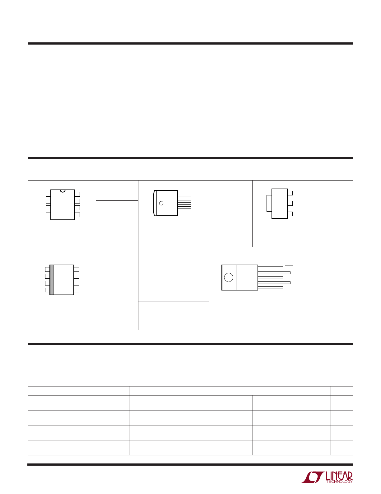
PACKAGE/ORDER INFORMATION
TOP VIEW
V
1
IN
I
2
LIM2
OUTPUT
3
SENSE
4
N8 PACKAGE
8-LEAD PDIP
θJA = 80°C/W TO 120°C/W DEPENDING
ON PC BOARD LAYOUT
V
8
IN
I
7
LIM4
SHDN
6
GND
5
ORDER
PART NUMBER
LT1175CN8
LT1175CN8-5
LT1175IN8
LT1175IN8-5
INPUT
FRONT VIEW
5
TAB
IS
θJA = 27°C/W TO 60°C/W DEPENDING
ON PC MOUNTING. SEE DATA SHEET
FOR DETAILS
4
3
2
1
Q PACKAGE
5-LEAD PLASTIC DD
SHDN Pin to VIN Pin Voltage .......................... 30V, –5V
Operating Junction Temperature Range
LT1175C..............................................0°C to 125°C
LT1175I.......................................... –40°C to 125°C
Ambient Operating Temperature Range
LT1175C................................................0°C to 70°C
LT1175I............................................ –40°C to 85°C
Storage Temperature Range ................. –65°C to 150°C
Lead Temperature (Soldering, 10 sec)..................300°C
UU
ORDER
SHDN
GND
INPUT
SENSE
OUTPUT
PART NUMBER
LT1175CQ
LT1175CQ-5
LT1175IQ
LT1175IQ-5
θJA = 50°C/W WITH BACKPLANE
AND 10cm2 TOPSIDE LAND
SOLDERED TO TAB
PART NUMBER
LT1175CST-5
LT1175IST-5
ORDER
TOP VIEW
1
V
IN
I
2
LIM2
OUTPUT
3
SENSE
4
S8 PACKAGE
8-LEAD PLASTIC SO
θJA = 60°C/W TO 100°C/W DEPENDING
ON PC BOARD LAYOUT
8
V
I
7
LIM4
SHDN
6
GND
5
PINS 1, 8 ARE INTERNALLY
CONNECTED TO DIE
ATTACH PADDLE FOR HEAT
IN
SINKING. ELECTRICAL
CONTACT CAN BE MADE TO
EITHER PIN. FOR BEST
THERMAL RESISTANCE,
PINS 1, 8 SHOULD BE
CONNECTED TO AN
EXPANDED LAND THAT IS
OVER AN INTERNAL OR
BACKSIDE PLANE.
SEE APPLICATIONS
INFORMATION
ORDER
PART NUMBER
LT1175CS8
LT1175CS8-5
LT1175IS8
LT1175IS8-5
S8 PART MARKING
1175
11755
1175I
1175I5
FRONT VIEW
5
4
3
2
TAB IS
INPUT
5-LEAD PLASTIC TO-220
θJA = 50°C/W, θJC = 5°C/W
1
T PACKAGE
SHDN
GND
INPUT
SENSE
OUTPUT
ORDER
PART NUMBER
LT1175CT
LT1175CT-5
LT1175IT
LT1175IT-5
Consult factory for Military grade parts.
ELECTRICAL CHARACTERISTICS
range, otherwise specifications are at TA = 25°C. V
OUT
The ● denotes specifications which apply over the operating temperature
= 5V, VIN = 7V, I
OUT
= 0, V
SHDN
= 3V, I
LIM2
and I
tied to VIN, TJ = 25°C,
LIM4
unless otherwise noted. To avoid confusion with “min” and “max” as applied to negative voltages, all voltages are shown as
absolute values except where polarity is not obvious.
PARAMETER CONDITIONS MIN TYP MAX UNITS
Feedback Sense Voltage Adjustable Part 3.743 3.8 3.857 V
Fixed 5V Part 4.93 5.0 5.075 V
Output Voltage Initial Accuracy Adjustable, Measured at 3.8V Sense 0.5 1.5 %
Fixed 5V 0.5 1.5 %
Output Voltage Accuracy (All Conditions) VIN – V
P = 0 to P
Quiescent Input Supply Current VIN – V
2
= 1V to VIN = 20V, I
OUT
, TJ = T
MAX
≤ 12V 45 65 µA
OUT
MIN
to T
= 0A to 500mA ● 1.5 2.5 %
OUT
(Note 3)
MAX
● 80 µA
Page 3
LT1 1 75
ELECTRICAL CHARACTERISTICS
range, otherwise specifications are at TA = 25°C. V
OUT
The ● denotes specifications which apply over the operating temperature
= 5V, VIN = 7V, I
OUT
= 0, V
SHDN
= 3V, I
LIM2
and I
tied to VIN, TJ = 25°C,
LIM4
unless otherwise noted. To avoid confusion with “min” and “max” as applied to negative voltages, all voltages are shown as
absolute values except where polarity is not obvious.
PARAMETER CONDITIONS MIN TYP MAX UNITS
GND Pin Current Increase with Load (Note 4) ● 10 20 µA/mA
Input Supply Current in Shutdown V
Shutdown Thresholds (Note 9) Either Polarity On SHDN Pin ● 0.8 2.5 V
SHDN Pin Current (Note 2) V
Output Bleed Current in Shutdown (Note 6) V
SENSE Pin Input Current (Adjustable Part Only, Current Flows Out of Pin) ● 75 150 nA
Dropout Voltage (Note 7) I
Current Limit (Note 11) VIN – V
Line Regulation (Note 10) VIN – V
Load Regulation (Note 5, 10) I
Thermal Regulation P = 0 to P
Output Voltage Temperature Drift TJ = 25°C to T
Note 1: Absolute Maximum Ratings are those values beyond which the life
of a device may be impaired.
Note 2: SHDN pin maximum positive voltage is 30V with respect to
and 13.5V with respect to GND. Maximum negative voltage is –20V
–V
IN
with respect to GND and –5V with respect to –V
Note 3: P
= 1.5W for 8-pin packages, and 6W for 5-pin packages. This
MAX
power level holds only for input-to-output voltages up to 12V, beyond
which internal power limiting may reduce power. See Guaranteed Current
Limit curve in Typical Performance Characteristics section. Note that all
conditions must be met.
Note 4: GND pin current increases because of power transistor base drive.
At low input-to-output voltages (< 1V) where the power transistor is in
saturation, GND pin current will be slightly higher. See Typical
Performance Characteristics.
Note 5: With I
= 0, at TJ > 125°C, power transistor leakage could
LOAD
increase higher than the 10µA to 25µA drawn by the output divider or fixed
voltage SENSE pin, causing the output to rise above the regulated value.
To prevent this condition, an internal active pull-up will automatically turn
on, but supply current will increase.
Note 6: This is the current required to pull the output voltage to within 1V
of ground during shutdown.
Note 7: Dropout voltage is measured by setting the input voltage equal to
the normal regulated output voltage and measuring the difference between
= 0V 10 20 µA
SHDN
= 0V to 10V (Flows Into Pin) ● 48 µA
SHDN
V
= –15V to 0V (Flows Into Pin) 1 4 µA
SHDN
= 0V, VIN = 15V 0.1 1 µA
OUT
● 25 µA
● 15 µA
(Fixed Voltage Only, Current Flows Out of Pin) ● 12 20 µA
= 25mA ● 0.1 0.2 V
OUT
= 100mA ● 0.18 0.26 V
I
OUT
= 500mA ● 0.5 0.7 V
I
OUT
Open, I
I
LIM2
I
Open, I
LIM4
I
, I
LIM2
LIM4
Open ● 390 600 975 mA
I
LIM2
Open ● 260 400 650 mA
I
LIM4
I
, I
LIM2
LIM4
= 0mA to 500mA ● 0.1 0.35 %
OUT
= 300mA ● 0.33 0.5 V
OUT
= 200mA ● 0.3 0.45 V
OUT
Open, I
= 1V to 12V ● 520 800 1300 mA
OUT
= 100mA ● 0.26 0.45 V
OUT
Open ● 130 200 325 mA
= 1V to VIN = 20V ● 0.003 0.015 %/V
OUT
(Notes 3, 8) 5-Pin Packages 0.04 0.1 %/W
MAX
8-Pin Packages 0.1 0.2 %/W
, or 25°C to T
JMIN
JMAX
VIN and V
. For currents between 100mA and 500mA, with both I
OUT
0.25 1.25 %
LIM
pins tied to VIN, maximum dropout can be calculated from
= 0.15 + 1.1Ω (I
V
DO
OUT
).
Note 8: Thermal regulation is a change in the output voltage caused by die
.
IN
temperature gradients, so it is proportional to chip power dissipation.
Temperature gradients reach final value in less than 100ms. Output
voltage changes after 100ms are due to absolute die temperature changes
and reference voltage temperature coefficient.
Note 9: The lower limit of 0.8V is guaranteed to keep the regulator in
shutdown. The upper limit of 2.5V is guaranteed to keep the regulator
active. Either polarity may be used, referenced to GND pin.
Note 10: Load and line regulation are measured on a pulse basis with
pulse width of 20ms or less to keep chip temperature constant. DC
regulation will be affected by thermal regulation (Note 8) and chip
temperature changes. Load regulation specification also holds for currents
or I
up to the specified current limit when I
LIM2
are left open.
LIM4
Note 11: Current limit is reduced for input-to-output voltage above 12V.
See the graph in Typical Performance Characteristics for guaranteed limits
above 12V.
Note 12: Operating at very large input-to-output differential voltages
(>15V) with load currents less than 5mA requires an output capacitor with
an ESR greater than 1Ω to prevent low level output oscillations.
3
Page 4
LT1 1 75
W
U
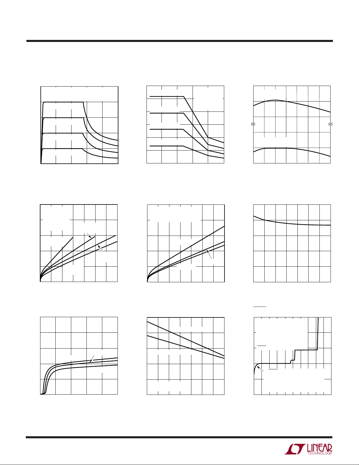
TYPICAL PERFORMANCE CHARACTERISTICS
Typical Current Limit
Characteristics
1.0
CURRENT LIMIT CHANGES ONLY SLIGHTLY
WITH TEMPERATURE SO CURVES ARE
REPRESENTATIVE OF ALL TEMPERATURES
0.8
I
, I
TIED TO V
LIM2
0.6
0.4
CURRENT (A)
0.2
I
I
I
LIM2
LIM2
LIM4
LIM
TIED TO V
TIED TO V
, I
LIM4
IN
IN
IN
OPEN
Guaranteed Current Limit
0.6
I
, I
TIED TO V
LIM2
I
LIM4
I
LIM2
I
LIM2
LIM
TIED TO V
TIED TO V
, I
OPEN
LIM4
IN
IN
0.5
0.4
0.3
CURRENT (A)
0.2
0.1
IN
CURVES REPRESENT MINIMUM
GUARANTEED
LIMITS AT ALL
TEMPERATURES
Output Voltage Temperature Drift
5.05
OUTPUT
FIXED 5V PART
5.00
4.95
3.84
VOLTAGE (V)
FEEDBACK VOLTAGE
ADJUSTABLE PART
3.80
0
5
0
INPUT-TO-OUTPUT DIFFERENTIAL VOLTAGE (V)
15
10
Minimum Input-to-Output Voltage
1.0
TJ = 25°C
REDUCED
V
IN
UNTIL OUTPUT
0.8
VOLTAGE
DROPS 1%
0.6
I
, I
LIM2
LIM4
OPEN
0.4
0.2
INPUT-TO-OUTPUT VOLTAGE (V)
0
0
0.2
0.1
OUTPUT CURRENT (A)
I
, I
LIM2
LIM4
TIED TO V
0.3
I
LIM2
IN
TO V
0.4
TIED
IN
0.5
Shutdown Input Current
25
20
15
10
INPUT CURRENT (µA)
5
0
0
TJ = 125°C
5
10
INPUT VOLTAGE (V)
TJ = –55°C
15
20
I
LIM4
TO V
0.6
TJ = 25°C
20
TIED
IN
1175 G01
1175 G04
1175 G07
0.7
0
5101520
25
0
INPUT-TO-OUTPUT DIFFERENTIAL VOLTAGE (V)
25
1175 G02
3.76
–50
0
–25
JUNCTION TEMPERATURE (°C)
50
25
75
100
125
1175 G03
SENSE Bias Current
Minimum Input-to-Output Voltage
1.0
VIN REDUCED UNTIL OUTPUT
VOLTAGE DROPS 1%.
, I
I
0.8
0.6
0.4
0.2
INPUT-TO-OUTPUT VOLTAGE (V)
0
0
TIED TO V
LIM2
LIM4
0.2
0.1
OUTPUT CURRENT (A)
IN
TJ = 125°C
TJ = –55°C
0.3
0.4
0.5
TJ = 25°C
0.6
1175 G05
0.7
Shutdown Thresholds
2.5
2.0
1.5
1.0
THRESHOLD (V)
0.5
DEVICE IS OFF
BELOW THRESHOLD
25
0
–50
POSITIVE THRESHOLD
NEGATIVE THRESHOLD
0
–25
TEMPERATURE (°C)
5025
100
125
1175 G08
75
(Adjustable Part)
100
80
60
40
CURRENT (nA)
20
0
–50
0
–25
TEMPERATURE (°C)
25
SHDN Pin Characteristics
15
VIN = 25V
CHARACTERISTICS DO NOT
CHANGE SIGNIFICANTLY WITH
10
TEMPERATURE, SO A SINGLE
CURVE IS SHOWN. POSITIVE
CURRENT FLOWS INTO
SHDN PIN
5
0
PIN CURRENT (µA)
–10
IF SHDN PIN IS NEGATIVE WITH
RESPECT TO INPUT VOLTAGE AND
–5
INPUT VOLTAGE IS LESS THAN 15V,
NEGATIVE BREAKOVER POINT WILL
BE ABOUT 8V BELOW –V
–15
–25 –20 –10 0
SHUTDOWN TO GROUND VOLTAGE (V)
–5 10 20
50
75
IN
5
125
100
1175 G06
15
25
1175 G09
4
Page 5

W
U
TYPICAL PERFORMANCE CHARACTERISTICS
LT1 1 75
GND pin Current
20
16
12
POWER
TRANSISTOR
8
IN DROPOUT
= –55°C
T
J
= 25°C
T
GROUND PIN CURRENT (mA)
4
0
J
0
0.1
VIN – V
OUT
T
= 25°C
J
VIN – V
T
0.2
OUTPUT CURRENT (A)
0.40.3
= 2V
= 25°C
J
0.5
OUT
0.6
≥ 3V
0.7
1175 G10
UUU
PIN FUNCTIONS
SENSE Pin: The SENSE pin is used in the adjustable
version to allow custom selection of output voltage, with
an external divider set to generate 3.8V at the SENSE pin.
Input bias current is typically 75nA flowing out of the pin.
Maximum forced voltage on the SENSE pin is 2V and –10V
with respect to GND pin.
The fixed 5V version utilizes the SENSE pin to give true
Kelvin connections to the load or to drive an external pass
transistor for higher output currents. Bias current out of
the 5V SENSE pin is approximately 12µA. Separating the
SENSE and OUTPUT pins also allows for a new loop
compensation technique described in the Applications
Information section.
SHDN Pin: The SHDN pin is specially configured to allow
it to be driven from either positive voltage logic or with
negative only logic. Forcing the SHDN pin 2V either above
or below the GND pin will turn the regulator on. This makes
it simple to connect directly to positive logic signals for
active low shutdown. If no positive voltages are available,
the SHDN pin can be driven below the GND pin to turn the
regulator on.
to a regulator “on” condition
absolute maximum ratings, the SHDN pin draws only a few
When left open, the SHDN pin will default low
. For all voltages below
Ripple Rejection
100
80
60
V
40
REJECTION (dB)
20
RIPPLE REJECTION IS RELATIVELY INDEPENDENT OF
INPUT VOLTAGE AND LOAD FOR CURRENTS BETWEEN
25mA AND 500mA. LARGER OUTPUT CAPACITORS DO
NOT IMPROVE REJECTION FOR FREQUENCIES BELOW
50kHz. AT VERY LIGHT LOADS, REJECTION WILL
IMPROVE WITH LARGER OUTPUT CAPACITORS
OUT
(ADJUSTABLE)
I
= 100mA
OUT
– V
V
IN
OUT
= 1µF TANT
C
OUT
0
10 1k 10k 1M
100 100k
V
(ADJUSTABLE)
WITH 0.1µF ACROSS
DIVIDER RESISTOR
= 12V
= 2V
FREQUENCY (Hz)
OUT
= 12V
V
OUT
(FIXED)
= 5V
1175 G11
microamperes of current (see Typical Performance Characteristics). Maximum voltage on the SHDN pin is 15V,
– 20V with respect to the GND pin and 35V, – 5V with
respect to the negative input pin.
I
Pins: The two current limit pins are emitter sections
LIM
of the power transistor. When left open, they float several
hundred millivolts above the negative input voltage. When
shorted to the input voltage, they increase current limit by
a minimum of 200mA for I
and 400mA for I
LIM2
LIM4
. These
pins must be connected only to the input voltage, either
directly or through a resistor.
OUTPUT Pin: The OUTPUT pin is the collector of the NPN
power transistor. It can be forced to the input voltage, to
ground or up to 2V positive with respect to ground without
damage or latchup (see Output Voltage Reversal in Applications Information section). The LT1175 has foldback
current limit, so maximum current at the OUTPUT pin is a
function of input-to-output voltage. See Typical Performance Characteristics.
GND Pin: The GND pin has a quiescent current of 45µA at
zero load current, increasing by approximately 10µA per
mA of output current. At 500mA output current, GND pin
current is about 5mA. Current flows into the GND pin.
5
Page 6

LT1 1 75
U
WUU
APPLICATIONS INFORMATION
Note to Reader: To avoid confusion when working with
negative voltages (is –6V more or less than –5V?), I have
decided to treat the LT1175 as if it were a positive
regulator and express all voltages as positive values, both
in text and in formulas. If you do the same and simply add
a negative sign to the eventual answer, confusion should
be avoided. Please don’t give me a hard time about
“preciseness” or “correctness.” I have to field phone calls
from around the world and this is my way of dealing with
a multitude of conventions. Thanks for your patience.
Setting Output Voltage
The LT1175 adjustable version has a feedback sense
voltage of 3.8V with a bias current of approximately 75nA
flowing out of the SENSE pin. To avoid output voltage
errors caused by this current, the output divider string
(see Figure 1) should draw about 25µA. Table 1 shows
suggested resistor values for a range of output voltages.
The second part of the table shows resistor values which
draw only 10µ A of current. Output voltage error caused by
bias current with the lower valued resistors is about 0.4%
maximum and with the higher values, about 1% maximum. A formula is also shown for calculating the resistors
for any output voltage.
Table 1
OUTPUT R1 R2 R1 R2
VOLTAGE I
5V 150k 47.5k 383k 121k
6V 150k 86.6k 383k 221k
8V 150k 165k 383k 422k
10V 150k 243k 383k 619k
12V 150k 324k 383k 825k
15V 150k 442k 383k 1.13M
= 25µA NEAREST 1% I
DIV
= 10µA NEAREST 1%
DIV
The LT1175-5 is a fixed 5V design with the SENSE pin
acting as a Kelvin connection to the output. Normally the
SENSE pin and the OUTPUT pin are connected directly
together, either close to the regulator or at the remote load
point.
SHUTDOWN
LOGIC
+
+
C
IN
INPUT
I
LIM2
I
LIM4
Figure 1. Typical LT1175 Adjustable Connection
> 2V OR < –2V TO
TURN REGULATOR ON
SHDN GND
LT1175-5
SENSE
OUT
R1
383k
1%
R2
825k
1%
C
OUT
≥ 0.1µF
V
OUT
–12V
1175 F01
Setting Current Limit
The LT1175 uses two I
pins to set current limit (typical)
LIM
at 200mA, 400mA, 600mA or 800mA. The corresponding
minimum guaranteed currents are 130mA, 260mA, 390mA
and 520mA. This allows the user to select a current limit
tailored to his specific application and prevents the situation where short-circuit current is many times higher than
full-load current. Problems with input supply overload or
excessive power dissipation in a faulted load are prevented. Power limiting in the form of foldback current limit
is built in and reduces current limit as a function of inputto-output voltage differential for differentials exceed
ing
14V. See the graph in Typical Performance Characteristics.
The LT1175 is guaranteed to be blowout-proof regardless
of current limit setting. The power limiting combined with
thermal shutdown protects the device from destructive
junction temperatures under all load conditions.
.
V
38
R
1
=
I
DIV
RV V
138
R
2
=
RV V
138
=
R2
38 1
=
I Desired
DIV
−
()
OUT
V
.
38
−
()
OUT
VRI
+
.
()
divider current
6
Shutdown
In shutdown, the LT1175 draws only about 10µ A. Special
.
Simple formula
()
circuitry is used to minimize increases in shutdown current at high temperatures, but a slight increase is seen
above 125°C. One option
.
FB
Taking SENSE pin bias
current into account
down on the output during shutdown. This means that the
output will fall slowly after shutdown is initiated, at a rate
determined by load current plus the 12µA internal load,
and the size of the output capacitor. Active pull-down is
not taken
was to actively pull
Page 7

LT1 1 75
U
WUU
APPLICATIONS INFORMATION
normally a good thing when the regulator is used by itself,
but it prevents the user from shutting down the regulator
when a second power source is connected to the LT1175
output. If active output pull-down is needed in shutdown,
it can be added externally with a depletion mode PFET as
shown in Figure 2. Note that the maximum pinch-off
voltage of the PFET must be less than the positive logic
high level to ensure that the device is completely off when
the regulator is active. The Motorola J177 device has
300Ω on resistance for zero gate source voltage.
3V TO 5V
+
SHDN GND
–V
IN
Figure 2. Active Output Pull-Down During Shutdown
INPUT
I
LIM2
I
LIM4
* MOTOROLA J177
PINCH-OFF VOLTAGE MUST BE LESS THAN
POSITIVE LOGIC HIGH VOLTAGE
LT1175-5
SENSE
OUT
Minimum Dropout Voltage
Dropout voltage is the minimum voltage required between
input and output to maintain proper output regulation. For
older 3-terminal regulator designs, dropout voltage was
typically 1.5V to 3V. The LT1175 uses a saturating power
transistor design which gives much lower dropout voltage, typically 100mV at light loads and 450mV at full load.
Special precautions were taken to ensure that this technique does not cause quiescent supply current to be high
under light load conditions. When the regulator input
voltage is too low to maintain a regulated output, the pass
transistor is driven hard by the error amplifier as it tries to
maintain regulation. The current drawn by the driver
transistor could be tens of milliamperes even with little or
no load on the output. This indeed was the case for older
IC designs that did not actively limit driver current when
the power transistor saturated. The LT1175 uses a new
antisaturation technique that prevents high driver current,
s
Q1*
d
C
OUT
≥ 0.1µF
1175 F02
yet allows the power transistor to approach its theoretical
saturation limit.
Output Capacitor
Several new regulator design techniques are used to make
the LT1175 extremely tolerant of output capacitor selection. Like most low dropout designs which use a collector
or drain of the power transistor to drive the output node,
the LT1175 uses the output capacitor as part of the overall
loop compensation. Older regulators generally required
the output capacitor to have a minimum value of 1µF to
100µF, a
0.1Ω to 1Ω and a
maximum
minimum
ESR (Effective Series Resistance) of
ESR in the range of 0.03Ω to
0.3Ω. These restrictions usually could be met only with
good quality solid tantalum capacitors. Aluminum capacitors have problems with high ESR unless much higher
values of capacitance are used (physically large). The ESR
of ceramic or film capacitors was too
low
, which made the
capacitance/ESR zero frequency too high to maintain
phase margin in the regulator. Even with optimum capacitors, loop phase margin was very low in previous designs
when output current was low. These problems led to a new
design technique for the LT1175 error amplifier and internal frequency compensation as shown in Figure 3.
A conventional regulator loop consists of error amplifier
A1, driver transistor Q2 and power transistor Q1. Added to
this basic loop are secondary loops generated by Q3 and
CF. A DC negative feedback current fed into the error
amplifier through Q3 and RN causes overall loop current
gain to be very low at light load currents. This is not a
problem because very little gain is needed at light loads. In
addition to low gain, the parasitic pole frequency at Q2
base is extended by the DC feedback. The combination of
these two effects dramatically improves loop phase margin at light loads and makes the loop tolerant of large ESR
in the output capacitor. With heavy loads, loop phase and
gain are not nearly as troublesome and large negative
feedback could degrade regulation. The logarithmic behavior of the base emitter voltage of Q1 reduces Q3 negative
feedback at heavy loads to prevent poor regulation.
In a conventional design, even with the nonlinear feedback, poor loop phase margin would occur at medium to
heavy loads if the ESR of the output capacitor fell below
7
Page 8

LT1 1 75
U
WUU
APPLICATIONS INFORMATION
LT1175
+
3.8V
–
A1
+
PATH
FEEDBACK
AT LIGHT
LOADS
AC
C
F
20pF
Q3
R
N
FEEDFORWARD
NEGATIVE DC
GND
R1
C
OUT
ESR
R2
Q2
R
0.5Ω
Q1
SENSE
OUT
C
PARASITIC
COLLECTOR
RESISTANCE
POWER
TRANSISTOR
LOAD
OUTPUT
–V
Figure 3
0.3Ω. This condition can occur with ceramic or film
capacitors which often have an ESR under 0.1Ω. With
previous designs, the user was forced to add a real resistor
in series with the capacitor to guarantee loop stability. The
LT1175 uses a unique AC feedforward technique to eliminate this problem. CF is a conventional feedforward capacitor often used in regulators to cancel the pole formed
by the output capacitor. It would normally be connected
from the regulated output node to the feedback node at the
R1/R2 junction or to an internal node on the amplifier as
shown. In this case, however, the capacitor is connected
to the internal structure of the power transistor. RC is the
unavoidable parasitic collector resistance of the power
transistor. Access to the node at the bottom of RC is
available only in monolithic structures where Kelvin connections can be made to the NPN buried collector layer.
The loop now responds as if RC were in series with the
output capacitor and good loop stability is achieved even
with extremely low ESR in the output capacitor.
R
LIM
CURRENT LIMIT
SENSE RESISTOR
IN
1175 F03
The end result of all this attention to loop stability is that
the output capacitor used with the LT1175 can range in
value from 0.1µ F to hundreds of microfarads, with an ESR
from 0Ω to 10Ω. This range allows the use of ceramic,
solid tantalum, aluminum and film capacitors over a wide
range of values.
The optimum output capacitor type for the LT1175 is still
solid tantalum, but there is considerable leeway in selecting the exact unit. If large load current transients are
expected, larger capacitors with lower ESR may be needed
to control worst-case output variation during transients. If
transients are not an issue, the capacitor can be chosen for
small physical size, low price, etc. Concerns about surge
currents in tantalum capacitors are not an issue for the
output capacitor because the LT1175 limits inrush current
to well below the level which can cause capacitor damage.
Surges caused by shorting the regulator output are also
not a problem because tantalum capacitors do not fail
8
Page 9

LT1 1 75
Die V V I
Maximum
T
T
I
V
JA IN OUT LOAD
A
JA
A
JA LOAD
OUT
Temp = T +
Power Dissipation =
T
=
T
A
MAX
MAX
θ
θ
θ
−
()()
−
−
()
+
U
WUU
APPLICATIONS INFORMATION
during a “shorting out” surge, only during a “charge up”
surge.
The output capacitor should be located within several
inches of the regulator. If remote sensing is used, the
output capacitor can be located at the remote sense node,
but the GND pin of the regulator should also be connected
to the remote site. The basic rule is to keep SENSE and
GND pins close to the output capacitor, regardless of
where it is.
Operating at very large input-to-output differential voltages (>5V) with load currents less than 5mA requires an
output capacitor with an ESR greater than 1Ω to prevent
low level output oscillations.
Input Capacitor
The LT1175 requires a separate input bypass capacitor
only if the regulator is located more than six inches from
the raw supply output capacitor. A 1µ F or larger tantalum
capacitor is suggested for all applications, but if low ESR
capacitors such as ceramic or film are used for the output
and
input capacitors, the input capacitor should be at least
three times the value of the output capacitor. If a solid
tantalum or aluminum electrolytic output capacitor is
used, the input capacitor is very noncritical.
High Temperature Operation
high. If a 4.8V output is pulled to 5V, for instance, the load
on the primary regulator would be (5V – 4.8V)/2kΩ =
100µA. This also means that if the internal pass transistor
leaks 50µA, the output voltage will be (50µA)(2kΩ) =
100mV high. This condition will not occur under normal
operating conditions, but could occur immediately after
an output short circuit had overheated the chip.
Thermal Considerations
The LT1175 is available in a special 8-pin surface mount
package which has Pins 1 and 8 connected to the die attach
paddle. This reduces thermal resistance when Pins 1 and
8 are connected to expanded copper lands on the PC
board. Table 2 shows thermal resistance for various
combinations of copper lands and backside or internal
planes. Table 2 also shows thermal resistance for the 5-pin
DD surface mount package and the 8-pin DIP and package.
Table 2. Package Thermal Resistance (°C/W)
LAND AREA DIP ST SO Q
Minimum 140 90 100 60
Minimum with 110 70 80 50
Backplane
1cm2 Top Plane 100 64 75 35
with Backplane
10cm2 Top Plane 80 50 60 27
with Backplane
The LT1175 is a micropower design with only 45µA
quiescent current. This could make it perform poorly at
high temperatures (>125°C), where power transistor leakage might exceed the output node loading current (5µ A to
15µ A). To avoid a condition where the output voltage drifts
uncontrolled high during a high temperature no-load
condition, the LT1175 has an active load which turns on
when the output is pulled above the nominal regulated
voltage. This load absorbs power transistor leakage and
maintains good regulation. There is one downside to this
feature, however. If the output is pulled high deliberately,
as it might be when the LT1175 is used as a backup to a
slightly higher output from a primary regulator, the LT1175
will act as an unwanted load on the primary regulator.
Because of this, the active pull-down is deliberately “weak.”
It can be modeled as a 2k resistor in series with an internal
clamp voltage when the regulator output is being pulled
To calculate die temperature, maximum power dissipation
or maximum input voltage, use the following formulas
with correct thermal resistance numbers from Table 2. For
through-hole TO-220 applications use θJA = 50°C/W
without a heat sink and θJA = 5°C/W + heat sink thermal
resistance when using a heat sink.
Maximum Input Voltage
for Thermal Considerations
9
Page 10

LT1 1 75
U
WUU
APPLICATIONS INFORMATION
T
= Maximum ambient temperature
A
T
= Maximum LT1175 die temperature (125°C for
MAX
commercial and industrial grades)
θ
= LT1175 thermal resistance, junction to ambient
JA
V
= Maximum continuous input voltage at maximum
IN
load current
I
= Maximum load current
LOAD
Example: LT1175S8 with I
VIN = 7V, TA = 60°C. Maximum die temperature for the
LT1175S8 is 125°C. Thermal resistance from Table 2 is
found to be 80°C/W.
Die Temperature = 60 + 80 (0.2A)(8 – 5) = 108°C
Maximum W
Power Dissipation =
Maximum Continuous
Input Voltage
(for Thermal Considerations)
= 200mA, V
LOAD
=
OUT
125–60
=
80
125–60
80 0 2
+=
.
()
= 5V,
081
.
59
V
NPN power transistor structure that has a parasitic diode
between the input and output of the regulator
. Reverse
voltages between input and output above 1V will damage
the regulator if large currents are allowed to flow. Simply
disconnecting the input source with the output held up will
not cause damage even though the input-to-output voltage will become slightly reversed.
High Frequency Ripple Rejection
The LT1175 will sometimes be powered from switching
regulators that generate the unregulated or quasi-regulated input voltage. This voltage will contain high frequency ripple that must be rejected by the linear regulator.
Special care was taken with the LT1175 to maximize high
frequency ripple rejection, but as with any micropower
design, rejection is strongly affected by ripple frequency.
The graph in the Typical Performance Characteristics
section shows 60dB rejection at 1kHz, but only 15dB
rejection at 100kHz for the 5V part. Photographs in Figures
4a and 4b show actual output ripple waveforms with
square wave and triwave input ripple.
Output Voltage Reversal
The LT1175 is designed to tolerate an output voltage
reversal of up to 2V. Reversal might occur, for instance, if
the output was shorted to a positive 5V supply. This would
almost surely destroy IC devices connected to the negative
output. Reversal could also occur during start-up if the
positive supply came up first and loads were connected
between the positive and negative supplies.
For these
reasons, it is always good design practice to add a reverse
biased diode from each regulator output to ground to limit
output voltage reversal
. The diode should be rated to
handle full negative load current for start-up situations, or
the short-circuit current of the positive supply if supply-tosupply shorts must be tolerated.
Input Voltage Lower Than Output
Linear Technology’s positive low dropout regulators
LT1121 and LT1129, will not draw large currents if the
input voltage is less than the output. These devices use a
lateral PNP power transistor structure that has 40V emitter
base breakdown voltage.
The LT1175, however, uses an
OUTPUT
20mV/DIV
INPUT
RIPPLE
100mV/DIV
OUTPUT
100mV/DIV
INPUT
RIPPLE
100mV/DIV
5µs/DIV 1175 F04
Figure 4a.
2µs/DIV 1175 F04
Figure 4b.
C
= 4.7µF TANT
OUT
= 1µF TANT
C
OUT
f = 50kHz
C
= 4.7µF TANT
OUT
= 1µF TANT
C
OUT
f = 100kHz
10
Page 11

LT1 1 75
L
ESR
f
FIL
rr
=
()
()
2
10
20π/
U
WUU
APPLICATIONS INFORMATION
To estimate regulator output ripple under different conditions, the following general comments should be helpful:
1. Output ripple at high frequency is only weakly affected
by load current or output capacitor size for medium to
heavy loads. At very light loads (<10mA), higher frequency ripple may be reduced by using larger output
capacitors.
2. A feedforward capacitor across the resistor divider
used with the adjustable part is effective in reducing
ripple only for output voltages greater than 5V and only
for frequencies less than 100kHz.
3. Input-to-output voltage differential has little effect on
ripple rejection until the regulator actually enters a
dropout condition of 0.2V to 0.6V.
If ripple rejection needs to be improved, an input filter can
be added. This filter can be a simple RC filter using a 1Ω
to 10Ω resistor. A 3.3Ω resistor for instance, combined
with a 0.3Ω ESR solid tantalum capacitor, will give an
additional 20dB ripple rejection. The size of the resistor
will be dictated by maximum load current. If the maximum
voltage drop allowable across the resistor is “VR,” and
maximum load current is I
loads, larger resistors and smaller capacitors can be used
, R = VR/I
LOAD
LOAD
. At light
to save space. At heavier loads an inductor may have to be
used in place of the resistor. The value of the inductor can
be calculated from:
ESR = Effective series resistance of filter capacitor. This
assumes that the capacitive reactance is small
compared to ESR, a reasonable assumption for
solid tantalum capacitors above 2.2µ F and 50kHz.
f = Ripple frequency
rr = Ripple rejection ratio of filter in dB
Example: ESR = 1.2Ω, f = 100kHz, rr = –25dB.
12
LH
=
FIL
63 10
.
.
5
25 20
−
10
/
34
=
µ
Solid tantalum capacitors are suggested for the filter to
keep filter Q fairly low. This prevents unwanted ringing at
the resonant frequency of the filter and oscillation problems with the filter/regulator combination.
U
PACKAGE DESCRIPTION
0.060
(1.524)
TYP
0.330 – 0.370
(8.382 – 9.398)
+0.012
0.143
–0.020
+0.305
3.632
()
–0.508
0.028 – 0.038
(0.711 – 0.965)
0.390 – 0.415
(9.906 – 10.541)
15° TYP
0.057 – 0.077
(1.447 – 1.955)
Information furnished by Linear Technology Corporation is believed to be accurate and reliable.
However, no responsibility is assumed for its use. Linear Technology Corporation makes no representation that the interconnection of its circuits as described herein will not infringe on existing patent rights.
Dimensions in inches (millimeters) unless otherwise noted.
Q Package
5-Lead Plastic DD Pak
(LTC DWG # 05-08-1461)
0.256
(6.502)
0.060
(1.524)
0.300
(7.620)
BOTTOM VIEW OF DD PAK
HATCHED AREA IS SOLDER PLATED
COPPER HEAT SINK
(1.524)
(1.905)
0.060
0.075
0.183
(4.648)
0.165 – 0.180
(4.191 – 4.572)
0.059
(1.499)
TYP
0.013 – 0.023
(0.330 – 0.584)
0.045 – 0.055
(1.143 – 1.397)
0.004
0.102
()
0.095 – 0.115
(2.413 – 2.921)
0.050 ± 0.012
(1.270 ± 0.305)
+0.008
–0.004
+0.203
–0.102
Q(DD5) 0396
11
Page 12

LT1 1 75
PACKAGE DESCRIPTION
U
Dimensions in inches (millimeters) unless otherwise noted.
N8 Package
8-Lead PDIP (Narrow 0.300)
(LTC DWG # 05-08-1510)
0.400*
(10.160)
MAX
876
0.255 ± 0.015*
(6.477 ± 0.381)
1234
0.300 – 0.325
(7.620 – 8.255)
0.065
(1.651)
0.009 – 0.015
(0.229 – 0.381)
+0.035
0.325
–0.015
+0.889
8.255
()
–0.381
*THESE DIMENSIONS DO NOT INCLUDE MOLD FLASH OR PROTRUSIONS.
MOLD FLASH OR PROTRUSIONS SHALL NOT EXCEED 0.010 INCH (0.254mm)
TYP
0.045 – 0.065
(1.143 – 1.651)
0.100 ± 0.010
(2.540 ± 0.254)
5
0.130 ± 0.005
(3.302 ± 0.127)
0.125
0.020
(3.175)
MIN
(0.508)
0.018 ± 0.003
(0.457 ± 0.076)
MIN
N8 1197
ST Package
3-Lead Plastic SOT-223
(LTC DWG # 05-08-1630)
S8 Package
8-Lead Plastic Small Outline (Narrow 0.150)
(LTC DWG # 05-08-1610)
0.228 – 0.244
(5.791 – 6.197)
0.010 – 0.020
(0.254 – 0.508)
0.008 – 0.010
(0.203 – 0.254)
*
DIMENSION DOES NOT INCLUDE MOLD FLASH. MOLD FLASH
SHALL NOT EXCEED 0.006" (0.152mm) PER SIDE
**
DIMENSION DOES NOT INCLUDE INTERLEAD FLASH. INTERLEAD
FLASH SHALL NOT EXCEED 0.010" (0.254mm) PER SIDE
× 45°
0.016 – 0.050
0.406 – 1.270
0°– 8° TYP
0.053 – 0.069
(1.346 – 1.752)
0.014 – 0.019
(0.355 – 0.483)
0.189 – 0.197*
(4.801 – 5.004)
8
1
0.248 – 0.264
(6.30 – 6.71)
0.116 – 0.124
(2.95 – 3.15)
7
2
6
3
5
0.150 – 0.157**
(3.810 – 3.988)
4
0.004 – 0.010
(0.101 – 0.254)
0.050
(1.270)
TYP
SO8 0996
10° – 16°
10°
MAX
0.012
(0.31)
MIN
0.390 – 0.415
(9.906 – 10.541)
0.460 – 0.500
(11.684 – 12.700)
0.057 – 0.077
(1.448 – 1.956)
0.010 – 0.014
(0.25 – 0.36)
0.0008 – 0.0040
(0.0203 – 0.1016)
10° – 16°
T Package
5-Lead Plastic TO-220 (Standard)
(LTC DWG # 05-08-1421)
0.147 – 0.155
(3.734 – 3.937)
DIA
0.230 – 0.270
(5.842 – 6.858)
0.570 – 0.620
(14.478 – 15.748)
0.330 – 0.370
(8.382 – 9.398)
0.260 – 0.320
(6.60 – 8.13)
0.028 – 0.038
(0.711 – 0.965)
(17.78 – 18.491)
0.152 – 0.202
(3.861 – 5.131)
0.071
(1.80)
MAX
0.165 – 0.180
(4.191 – 4.572)
0.700 – 0.728
0.135 – 0.165
(3.429 – 4.191)
0.620
(15.75)
TYP
0.025 – 0.033
(0.64 – 0.84)
0.181
(4.60)
NOM
0.045 – 0.055
(1.143 – 1.397)
0.095 – 0.115
(2.413 – 2.921)
0.013 – 0.023
(0.330 – 0.584)
0.155 – 0.195
(3.937 – 4.953)
T5 (TO-220) 0398
0.264 – 0.287
(6.71 – 7.29)
0.130 – 0.146
(3.30 – 3.71)
0.090
(2.29)
NOM
RELATED PARTS
LT1121 150mA Positive Micropower Low Dropout
Regulator with Shutdown
LT1129 700mA Positive Micropower Low Dropout
Regulator with Shutdown
LT1185 3A Negative Low Dropout Regulator
LT1521 300mA Positive Micropower Low Dropout
Regulator with Shutdown
LT1529 3A Positive Micropower Low Dropout
Regulator with Shutdown
0.033 – 0.041
(0.84 – 1.04)
ST3 (SOT-233) 0792
12
Linear Technology Corporation
1630 McCarthy Blvd., Milpitas, CA 95035-7417
(408) 432-1900 ● FAX: (408) 434-0507
●
www.linear-tech.com
1175fc LT/TP 0399 2K REV C • PRINTED IN USA
LINEAR TECHNOLOGY CORPORATION 1995
 Loading...