

Datasheet LT1130ACNW, LT1134ACSW, LT1134ACN, LT1133AISW, LT1133ACSW Datasheet (Linear Technology)
...Page 1
FEATURES
■
ESD Protection over ±10kV
(±15kV IEC-1000-4-2 for LT1133A, LT1137A
and LT1141A)
■
Uses Small Capacitors: 0.1µF, 0.2µF
■
1µA Supply Current in SHUTDOWN
■
120kBaud Operation for RL = 3k, CL = 2500pF
■
250kBaud Operation for RL = 3k, CL = 1000pF
■
CMOS Comparable Low Power
■
Easy PC Layout: Flowthrough Architecture
■
Rugged Bipolar Design: Absolutely No Latchup
■
Outputs Assume a High Impedance State When Off
or Powered Down
■
Improved Protection: RS232 I/O Lines Can Be Forced
to ±30V Without Damage
■
Output Overvoltage Does Not Force Current Back
into Supplies
■
Available in SO and SSOP Packages
LT1130A/LT1140A Series
Advanced Low Power
5V RS232 Drivers/Receivers
with Small Capacitors
U
DESCRIPTIO
The LT®1130A/LT1140A series of RS232 drivers/receivers features special bipolar construction techniques which
protect the drivers and receivers beyond the fault conditions stipulated for RS232. Driver outputs and receiver
inputs can be shorted to ±30V without damaging the
device or the power supply generator. In addition, the
RS232 I/O pins are resilient to multiple ±10kV ESD strikes.
An advanced driver output stage operates up to 250kbaud
while driving heavy capacitive loads. Supply current is
typically 12mA, competitive with CMOS devices.
Several members of the series include flexible operating
mode controls. The DRIVER DISABLE pin disables the
drivers and the charge pump, the ON/OFF pin shuts down
all circuitry. While shut down, the drivers and receivers
assume high impedance output states.
, LTC and LT are registered trademarks of Linear Technology Corporation.
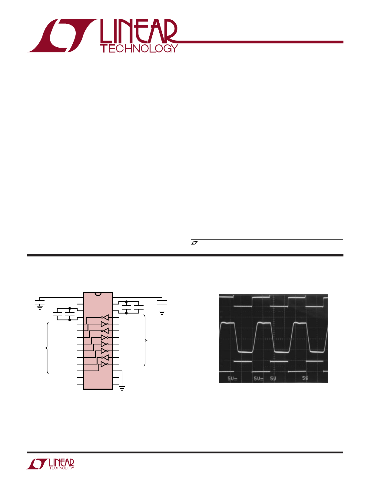
U
TYPICAL APPLICATIO
Basic Operation
+
1
V
5V V
RX IN
RX IN
RX IN
RX IN
RX IN
2
CC
3
LT1137A
4
5
6
7
8
9
10
11
12
13
14
0.1µF
0.1µF
× 2
DRIVER OUT
DRIVER OUT
TO LINE
DRIVER OUT
ON/OFF = 5V
LT1130A 5-Driver/5-Receiver RS232 Transceiver
LT1131A 5-Driver/4-Receiver RS232 Transceiver w/Shutdown
LT1132A 5-Driver/3-Receiver RS232 Transceiver
LT1133A 3-Driver/5-Receiver RS232 Transceiver
LT1134A 4-Driver/4-Receiver RS232 Transceiver
LT1135A 5-Driver/3-Receiver RS232 Transceiver w/o Charge Pump
28
V
27
26
25
DRIVER IN
24
RX OUT
23
DRIVER IN
22
RX OUT
21
RX OUT
20
RX OUT
19
DRIVER IN
18
RX OUT
17
GND
16
DRIVER DISABLE
15
–
1130A • TA01
0.1µF
× 2
TO LOGIC
0.1µF
Output Waveforms
RECEIVER
OUTPUT
= 50pF
C
L
DRIVER
R
OUTPUT
RL = 3k
= 2500pF
C
L
INPUT
LT1130A • TA02
LT1136A 4-Driver/5-Receiver RS232 Transceiver w/Shutdown
LT1137A 3-Driver/5-Receiver RS232 Transceiver w/Shutdown
LT1138A 5-Driver/3-Receiver RS232 Transceiver w/Shutdown
LT1139A 4-Driver/4-Receiver RS232 Transceiver w/Shutdown
LT1140A 5-Driver/3-Receiver RS232 Transceiver w/o Charge Pump
LT1141A 3-Driver/5-Receiver RS232 Transceiver w/o Charge Pump
1
Page 2
LT1130A/LT1140A Series
W
O
A
LUTEXI TIS
S
Supply Voltage (VCC) ................................................ 6V
V+........................................................................ 13.2V
V– (Note 7) ....................................................... –13.2V
Input Voltage
Driver ........................................................... V– to V
Receiver ............................................... – 30V to 30V
On/Off Pin............................................. –0.3V to 12V
Driver Disable Pin................... –0.3V to (VCC + 0.3V)
Output Voltage
Driver .................................................... – 30V to 30V
A
WUW
U
(Note 1)
ARB
G
Short-Circuit Duration
V+................................................................... 30 sec
V–................................................................... 30 sec
Driver Output.............................................. Indefinite
+
Receiver Output.......................................... Indefinite
Operating Temperature Range
LT113XAC/LT114XAC ............................ 0°C to 70°C
LT113XAI/LT114XAI............................. – 40° to 85°C
Storage Temperature Range ................ –65°C to 150°C
Lead Temperature (Soldering, 10 sec)................. 300°C
Receiver ................................. – 0.3V to (VCC + 0.3V)
U
PRODUCT SELECTIO TABLE
Part Number Power Supply Voltages* Shutdown Driver Disable Drivers Receivers External Components
LT1130A 5 No No 5 5 4 Capacitors
LT1131A 5 Yes Yes 5 4 4 Capacitors
LT1132A 5 No No 5 3 4 Capacitors
LT1133A** 5 No No 3 5 4 Capacitors
LT1134A 5 No No 4 4 4 Capacitors
LT1135A 5, 12, –12 No No 5 3 None
LT1136A 5 Yes Yes 4 5 4 Capacitors
LT1137A** 5 Yes Yes 3 5 4 Capacitors
LT1138A 5 Yes Yes 5 3 4 Capacitors
LT1139A 5, 12 Yes No 4 4 2 Capacitors
LT1140A 5, 12, –12 Yes Yes 5 3 None
LT1141A** 5, 12, –12 Yes Yes 3 5 None
*The LT1130A, LT1131A, LT1132A, LT1134A, LT1136A, LT1137A and LT1138A can operate with 5V and 12V supplies and two external capacitors.
**Meets ±15kV ESD air gap discharge and ±8kV contact methods per IEC-1000-4-2.
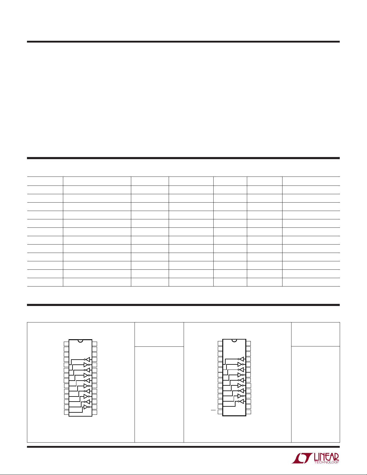
PACKAGE
5-DRIVER/5-RECEIVER
+
V
5V V
CC
+
C1
–
C1
DRIVER OUT
RX IN
DRIVER OUT
RX IN
DRIVER OUT
RX IN
DRIVER OUT
DRIVER OUT
10
11
RX IN
12
13
RX IN
14
NW PACKAGE
28-LEAD PDIP
T
= 150°C, θJA = 56°C/W (NW)
JMAX
= 150°C, θJA = 68°C/W (SW)
T
JMAX
2
/
O
RDER I FOR ATIO
TOP VIEW
–
1
LT1130A
2
3
4
5
6
7
8
9
28
V
–
27
C2
+
26
C2
25
DRIVER IN
24
RX OUT
23
DRIVER IN
22
RX OUT
21
DRIVER IN
20
RX OUT
19
DRIVER IN
18
RX OUT
17
DRIVER IN
16
RX OUT
15
GND
SW PACKAGE
28-LEAD PLASTIC SO WIDE
WU
U
ORDER PART
NUMBER
LT1130ACNW
LT1130ACSW
LT1130AISW
5-DRIVER/4-RECEIVER WITH SHUTDOWN
TOP VIEW
5V V
C1
C1
DRIVER OUT
RX IN
DRIVER OUT
RX IN
DRIVER OUT
RX IN
DRIVER OUT
RX IN
DRIVER OUT
ON/OFF
NW PACKAGE
28-LEAD PDIP
T
T
+
V
1
LT1131A
2
CC
+
3
–
4
5
6
7
8
9
10
11
12
13
14
28-LEAD PLASTIC SO WIDE
= 150°C, θJA = 56°C/W (NW)
JMAX
= 150°C, θJA = 68°C/W (SW)
JMAX
–
28
V
27
C2
26
C2
25
DRIVER IN
24
RX OUT
23
DRIVER IN
22
RX OUT
21
DRIVER IN
20
RX OUT
19
DRIVER IN
18
RX OUT
17
DRIVER IN
16
GND
15
DRIVER DISABLE
SW PACKAGE
–
+
ORDER PART
NUMBER
LT1131ACNW
LT1131ACSW
Page 3
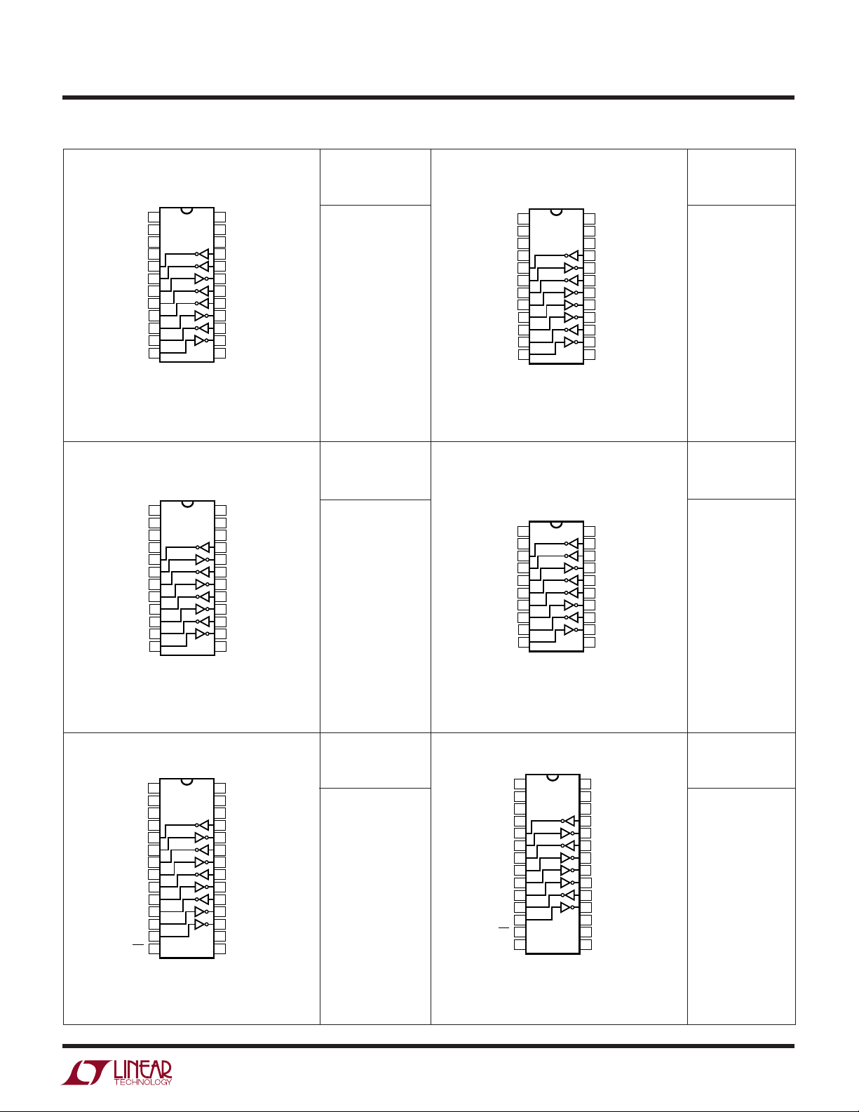
LT1130A/LT1140A Series
1
2
3
4
5
6
7
8
9
10
11
12
TOP VIEW
24
23
22
21
20
19
18
17
16
15
14
13
V
–
C2
–
C2
+
DRIVER IN
RX OUT
DRIVER IN
RX OUT
RX OUT
RX OUT
DRIVER IN
RX OUT
GND
SW PACKAGE
24-LEAD PLASTIC SO WIDE
N PACKAGE
24-LEAD PDIP
LT1133A
V
+
5V V
CC
C1
+
C1
–
DRIVER OUT
RX IN
DRIVER OUT
RX IN
RX IN
RX IN
DRIVER OUT
RX IN
1
2
3
4
5
6
7
8
9
10
TOP VIEW
20
19
18
17
16
15
14
13
12
11
–12V V
–
DRIVER IN
DRIVER IN
RX OUT
DRIVER IN
DRIVER IN
RX OUT
DRIVER IN
RX OUT
GND
SW PACKAGE
20-LEAD PLASTIC SO WIDE
N PACKAGE
20-LEAD PDIP
12V V
+
5V V
CC
DRIVER OUT
DRIVER OUT
RX IN
DRIVER OUT
DRIVER OUT
RX IN
DRIVER OUT
RX IN
LT1135A
PACKAGE
5-DRIVER/3-RECEIVER
+
V
1
5V V
2
CC
+
C1
3
–
C1
DRIVER OUT
DRIVER OUT
DRIVER OUT
DRIVER OUT
DRIVER OUT
DRIVER OUT
DRIVER OUT
DRIVER OUT
DRIVER OUT
4
5
6
RX IN
7
8
9
RX IN
10
11
RX IN
12
N PACKAGE
24-LEAD PDIP
T
= 150°C, θJA = 58°C/W (N)
JMAX
= 150°C, θJA = 80°C/W (SW)
T
JMAX
4-DRIVER/4-RECEIVER
+
V
5V V
CC
+
C1
–
C1
RX IN
RX IN
RX IN
10
11
RX IN
12
N PACKAGE
24-LEAD PDIP
/
O
RDER I FOR ATIO
TOP VIEW
–
24
V
LT1132A
24-LEAD PLASTIC SO WIDE
TOP VIEW
1
LT1134A
2
3
4
5
6
7
8
9
24-LEAD PLASTIC SO WIDE
23
C2
22
C2
21
DRIVER IN
20
DRIVER IN
19
RX OUT
18
DRIVER IN
17
DRIVER IN
16
RX OUT
15
DRIVER IN
14
RX OUT
13
GND
SW PACKAGE
–
24
V
23
C2
22
C2
21
DRIVER IN
20
RX OUT
19
DRIVER IN
18
RX OUT
17
DRIVER IN
16
RX OUT
15
DRIVER IN
14
RX OUT
13
GND
SW PACKAGE
–
+
–
+
WU
U
ORDER PART
NUMBER
LT1132ACN
LT1132ACSW
LT1132AISW
ORDER PART
NUMBER
LT1134ACN
LT1134ACSW
LT1134AIN
LT1134AISW
3-DRIVER/5-RECEIVER
T
= 150°C, θJA = 58°C/W (N)
JMAX
= 150°C, θJA = 80°C/W (SW)
T
JMAX
5-DRIVER/3-RECEIVER
WITHOUT CHARGE PUMP
ORDER PART
NUMBER
LT1133ACN
LT1133ACSW
LT1133AISW
ORDER PART
NUMBER
LT1135ACN
LT1135ACSW
= 150°C, θJA = 79°C/W (N)
5V V
DRIVER OUT
RX IN
DRIVER OUT
RX IN
RX IN
RX IN
DRIVER OUT
RX IN
ON/OFF
G PACKAGE
T
JMAX
= 150°C, θJA = 85°C/W (SW)
T
JMAX
TOP VIEW
+
V
1
LT1137A
2
CC
+
C1
3
–
C1
4
5
6
7
8
9
10
11
12
13
NC
14
NW PACKAGE
28-LEAD PDIP
T
= 150°C, θJA = 96°C/W (G)
JMAX
= 150°C, θJA = 56°C/W (NW)
T
JMAX
= 150°C, θJA = 68°C/W (SW)
T
JMAX
–
28
V
–
27
C2
+
26
C2
25
DRIVER IN
24
RX OUT
23
DRIVER IN
22
RX OUT
21
RX OUT
20
RX OUT
19
DRIVER IN
18
RX OUT
17
GND
16
DRIVER DISABLE
15
NC
SW PACKAGE
28-LEAD PLASTIC SO WIDE
ORDER PART
NUMBER
LT1137ACG
LT1137ACNW
LT1137ACSW
LT1137AIG
LT1137AINW
LT1137AISW
3
= 150°C, θJA = 58°C/W (N)
T
JMAX
= 150°C, θJA = 80°C/W (SW)
T
JMAX
ORDER PART
TOP VIEW
+
V
1
5V V
DRIVER OUT
RX IN
DRIVER OUT
RX IN
DRIVER OUT
RX IN
DRIVER OUT
RX IN
RX IN
ON/OFF
NW PACKAGE
28-LEAD PDIP
LT1136A
2
CC
+
C1
3
–
C1
4
5
6
7
8
9
10
11
12
13
14
T
T
JMAX
JMAX
28-LEAD PLASTIC SO WIDE
= 150°C, θJA = 56°C/W (NW)
= 150°C, θJA = 68°C/W (SW)
–
28
V
27
C2
26
C2
25
DRIVER IN
24
RX OUT
23
DRIVER IN
22
RX OUT
21
DRIVER IN
20
RX OUT
19
DRIVER IN
18
RX OUT
17
RX OUT
16
GND
15
DRIVER DISABLE
SW PACKAGE
–
+
NUMBER
LT1136ACNW
LT1136ACSW
3-DRIVER/5-RECEIVER WITH SHUTDOWN4-DRIVER/5-RECEIVER WITH SHUTDOWN
28-LEAD PLASTIC SSOP
Page 4
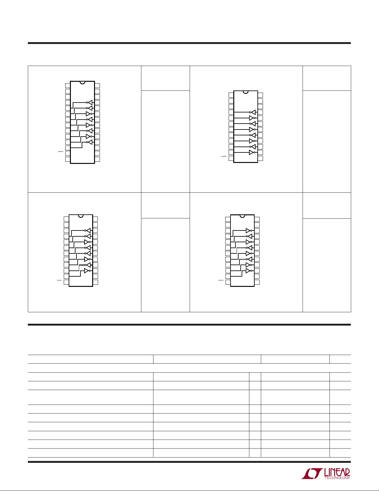
LT1130A/LT1140A Series
1
2
3
4
5
6
7
8
9
10
11
12
TOP VIEW
24
23
22
21
20
19
18
17
16
15
14
13
V
–
C
–
C
+
DRIVER IN
RX OUT
DRIVER IN
RX OUT
DRIVER IN
RX OUT
DRIVER IN
RX OUT
GND
SW PACKAGE
24-LEAD PLASTIC SO WIDE
N PACKAGE
24-LEAD PDIP
LT1139A
N.C.
5V V
CC
12V INPUT
DRIVER OUT
RX IN
DRIVER OUT
RX IN
DRIVER OUT
RX IN
DRIVER OUT
RX IN
ON/OFF
/
PACKAGE
O
RDER I FOR ATIO
5-DRIVER/3-RECEIVER WITH SHUTDOWN
TOP VIEW
+
V
5V V
CC
+
C1
–
C1
DRIVER OUT
DRIVER OUT
RX IN
DRIVER OUT
RX IN
DRIVER OUT
RX IN
DRIVER OUT
ON/OFF
NC
G PACKAGE
28-LEAD PLASTIC SSOP
T
JMAX
T
JMAX
T
JMAX
1
LT1138A
2
3
4
5
6
7
8
9
10
11
12
13
14
NW PACKAGE
28-LEAD PDIP
= 150°C, θJA = 96°C/W (G)
= 150°C, θJA = 56°C/W (NW)
= 150°C, θJA = 68°C/W (SW)
–
28
V
–
27
C2
+
26
C2
25
DRIVER IN
24
DRIVER IN
23
RX OUT
22
DRIVER IN
21
RX OUT
20
DRIVER IN
19
RX OUT
18
DRIVER IN
17
GND
16
DRIVER DISABLE
15
NC
SW PACKAGE
28-LEAD PLASTIC SO WIDE
5-DRIVER/3-RECEIVER WITH SHUTDOWN
WITHOUT CHARGE PUMP
TOP VIEW
+
12V V
1
5V V
N.C.
DRIVER OUT
DRIVER OUT
RX IN
DRIVER OUT
DRIVER OUT
RX IN
DRIVER OUT
RX IN
ON/OFF
N PACKAGE
24-LEAD PDIP
T
LT1140A
2
CC
3
4
5
6
7
8
9
10
11
12
SW PACKAGE
24-LEAD PLASTIC SO WIDE
T
= 150°C, θJA = 58°C/W (N)
JMAX
= 150°C, θJA = 80°C/W (SW)
JMAX
Consult factory for Industrial and Military grade parts.
24
–12V V
23
N.C.
22
DRIVER IN
21
DRIVER IN
20
RX OUT
19
DRIVER IN
18
DRIVER IN
17
RX OUT
16
DRIVER IN
15
RX OUT
14
GND
13
DRIVER DISABLE
–
WU
U
ORDER PART
NUMBER
LT1138ACG
LT1138ACNW
LT1138ACSW
LT1138AIG
ORDER PART
NUMBER
LT1140ACN
LT1140ACSW
4-DRIVER/4-RECEIVER WITH SHUTDOWN
WITH 12V AND 5V SUPPLIES
T
= 150°C, θJA = 58°C/W (N)
JMAX
= 150°C, θJA = 80°C/W (SW)
T
JMAX
3-DRIVER/5-RECEIVER WITH SHUTDOWN
WITHOUT CHARGE PUMP
TOP VIEW
12V V
5V V
N.C.
RX IN
DRIVER OUT
RX IN
DRIVER OUT
RX IN
DRIVER OUT
RX IN
RX IN
ON/OFF
N PACKAGE
24-LEAD PDIP
T
T
+
1
LT1141A
2
CC
3
4
5
6
7
8
9
10
11
12
SW PACKAGE
24-LEAD PLASTIC SO WIDE
= 150°C, θJA = 58°C/W (N)
JMAX
= 150°C, θJA = 80°C/W (SW)
JMAX
24
–12V V
23
N.C.
22
RX OUT
21
DRIVER IN
20
RX OUT
19
DRIVER IN
18
RX OUT
17
DRIVER IN
16
RX OUT
15
RX OUT
14
GND
13
DRIVER DISABLE
–
ORDER PART
NUMBER
LT1139ACN
LT1139ACSW
ORDER PART
NUMBER
LT1141ACN
LT1141ACSW
LECTRICAL C CHARA TERIST
E
temperature range, otherwise specifications are at T
ICS
The ● denotes the specifications which apply over the full operating
= 25°C. (Note 2)
A
PARAMETER CONDITIONS MIN TYP MAX UNITS
Power Supply Generator
V+ Output 8.6 V
V– Output –7.8 V
5V VCC Supply Current: LT1130A, LT1131A, LT1132A, (Note 3) ● 15 25 mA
LT1133A, LT1134A, LT1136A, LT1138A
5V VCC Supply Current: LT1135A, LT1140A, LT1141A (Note 3), V+ = 12V, V– = –12V ● 815 mA
5V VCC Supply Current: LT1137A (Note 3) ● 12 17 mA
5V VCC Supply Current: LT1139A (Note 3), V+ = 12V ● 815 mA
12V V+ Supply Current: LT1135A, LT1140A, LT1141A (Note 3), V– = –12V ● 14 mA
12V V+ Supply Current: LT1139A (Note 3) ● 610 mA
–12V V– Supply Current: LT1135A, LT1140A, LT1141A (Note 3) V+ = 12V ● 26 mA
4
Page 5

LT1130A/LT1140A Series
LECTRICAL C CHARA TERIST
E
temperature range, otherwise specifications are at T
PARAMETER CONDITIONS MIN TYP MAX UNITS
Supply Current when OFF (VCC) Shutdown (Note 4) ● 110 µA
Supply Rise Time C1, C2, C+, C– = 1.0µF 2.0 ms
Shutdown to Turn-On C
ON/OFF Pin Thresholds Input Low Level (Device Shut Down) ● 1.4 0.8 V
ON/OFF Pin Current 0V ≤ V
DRIVER DISABLE Pin Thresholds Input Low Level (Drivers Enabled) ● 1.4 0.8 V
DRIVER DISABLE Pin Current 0V ≤ V
Oscillator Frequency 130 kHz
Any Driver
Output Voltage Swing Load = 3k to GND Positive ● 5 7.3 V
Logic Input Voltage Level Input Low Level (V
Logic Input Current 0.8V ≤ VIN ≤ 2V ● 520 µA
Output Short-Circuit Current V
Output Leakage Current Shutdown V
Data Rate RL = 3k, CL = 2500pF 120 kbaud
Slew Rate RL = 3k, CL = 51pF 15 30 V/µs
Propagation Delay Output Transition tHL High to Low (Note 5) 0.6 1.3 µs
Any Receiver
Input Voltage Thresholds Input Low Threshold (V
Hysteresis ● 0.1 0.4 1 V
Input Resistance –10V < VIN < 10V 3 5 7 kΩ
Output Voltage Output Low, I
Output Leakage Current Shutdown (Note 4) 0 ≤ V
Output Short-Circuit Current Sinking Current, V
Propagation Delay Output Transition tHL High to Low (Note 6) 250 600 ns
Note 1: Absolute Maximum Ratings are those values beyond which the life
of the device may be impaired.
Note 2: Testing done at VCC = 5V and V
Note 3: Supply current is measured with driver and receiver outputs
unloaded and the driver inputs tied high.
Note 4: Supply current and driver leakage current measurements in shut-
down are performed with V
using DRIVER DISABLE are performed with V
LT1135, LT1139, LT1140 and LT1141 with 12V supplies, V
200µA for V
forced to ±25V.
OUT
= 0.1V. Supply current measurements
ON/OFF
ON/OFF
= 3V.
DRIVER DISABLE
The ● denotes the specifications which apply over the full operating
ICS
= 25°C. (Note 2)
A
Driver Disable 4 mA
+
, C– = 0.1µF, C1, C2 = 0.2µF 0.2 ms
Input High Level (Device Enabled)
≤ 5V ● –15 80 µA
ON/OFF
Input High Level (Drivers Disabled)
DRIVER DISABLE
Negative
Input High Level (V
= 0V ±9 ±17 mA
OUT
R
= 3k, CL = 1000pF 250 kbaud
L
R
= 3k, CL = 2500pF (Note 8) 6 V/µs
L
Output Transition t
Input High Threshold (V
Output High, I
Sourcing Current, V
Output Transition t
= 3V. For
leakage is
OUT
≤ 5V ● – 10 500 µA
= High) ● 1.4 0.8 V
OUT
= Low) ● 2 1.4 V
OUT
= ±30V (Note 4) ● 10 100 µA
OUT
Low to High 0.5 1.3 µs
LH
= High) ● 0.8 1.3 V
OUT
= Low) ● 1.7 2.4 V
OUT
= –1.6mA ● 0.2 0.4 V
OUT
= 160µA (VCC = 5V) ● 3.5 4.2 V
OUT
≤ V
OUT
CC
= V
OUT
CC
= 0V 10 20 mA
OUT
Low to High 350 600 ns
LH
Note 5: For driver delay measurements, RL = 3k and CL = 51pF. Trigger
points are set between the driver’s input logic threshold and the output
transition to the zero crossing (t
Note 6: F
are set between the receiver’s input logic threshold and the output
transition to standard TTL/CMOS logic threshold (t
and t
Note 7: For LT1133A/LT1137A, absolute maximum externally applied
V– = –6.5V. Internal charge pump will drive this pin to a higher negative voltage.
Note 8: For LT1137A, 4V/µs minimum.
or receiver delay measurements, CL = 51pF. Trigger points
= 1.7V to 0.8V).
LH
● 2.4 1.4 V
● 2.4 1.4 V
● –6.5 –5 V
● 110 µA
–20 –10 mA
= 1.4V to 0V and tLH = 1.4V to 0V).
HL
= 1.3V to 2.4V
HL
5
Page 6

LT1130A/LT1140A Series
DATA RATE (kBaud)
0
0
SUPPLY CURRENT (mA)
20
30
40
50
60
70
25
50
75 100
LT1130A • TPC03
125
80
90
100
10
150
5 DRIVER
R
L
= 3k
C
L
= 2500pF
3 DRIVER
R
L
= 3k
C
L
= 2500pF
UW
LPER
R
F
O
ATYPICA
CCHARA TERIST
E
C
ICS
Driver Output Voltage
10
RL = 3k
8
6
4
2
0
–2
–4
–6
DRIVER OUTPUT VOLTAGE (V)
–8
–10
–55
–25
100
10
1
SUPPLY CURRENT (µA)
OUTPUT HIGH
= 5.5V
V
CC
VCC = 5V
V
= 4.5V
CC
VCC = 4.5V
V
CC
V
= 5.5V
CC
OUTPUT LOW
25
0
TEMPERATURE (°C)
= 5V
50
75
100
LT1130A • TPC01
125
3.00
2.75
2.50
2.25
2.00
1.75
1.50
1.25
THRESHOLD VOLTAGE (V)
1.00
0.75
0.50
–55
–25
INPUT HIGH
INPUT LOW
50
25
0
TEMPERATURE (°C)
Supply Current in Driver Disable
5
4
3
2
SUPPLY CURRENT (mA)
1
75
100
LT1137A • TPC02
Supply Current vs Data RateReceiver Input Thresholds
125
Driver Disable ThresholdSupply Current in Shutdown
3.0
2.5
2.0
1.5
1.0
THRESHOLD VOLTAGE (V)
0.5
0.1
–55
ON/OFF Thresholds
3.0
2.5
2.0
1.5
1.0
THRESHOLD VOLTAGE (V)
0.5
0
–55
6
–25 0 25 50
TEMPERATURE (°C)
ON THRESHOLD
–25 0
OFF THRESHOLD
25 75
TEMPERATURE (°C)
75 100 125
LT1137A • TPC04
50 100 125
LT1137A • TPC07
0
–55
0
–25
TEMPERATURE (°C)
Supply Current
50
45
5 DRIVER
40
35
3 DRIVER
30
25
1 DRIVER
20
NO LOAD
15
SUPPLY CURRENT (mA)
10
5
0
–55
0
–25
TEMPERATURE (°C)
50
25
75
100
LT1137A • TPC05
125
0
–55
–25 0
50 100 125
25 75
TEMPERATURE (°C)
LT1137A • TPC06
Driver Leakage in Shutdown
100
10
V
= 30V
1
LEAKAGE CURRENT (µA)
50
25
75
100
LT1130A • TPC08
125
0.1
–55 0
–25
TEMPERATURE (°C)
OUT
V
= –30V
OUT
50
25
75
100
LT1137A • TPC09
125
Page 7

LPER
F
O
R
ATYPICA
UW
CCHARA TERIST
E
C
LT1130A/LT1140A Series
ICS
DRIVER
OUTPUT HIGH
RL = 3k
DRIVER
OUTPUT LOW
R
= 3k
L
Driver Short-Circuit Current
30
25
20
15
10
SHORT-CIRCUIT CURRENT (mA)
5
0
–55
–25 0
25 75
TEMPERATURE (°C)
Shutdown to Driver Output
10
5
0
–5
–10
+
ISC
–
ISC
50 100 125
LT1137A • TPC10
50
40
30
20
10
SHORT-CIRCUIT CURRENT (mA)
DRIVER OUTPUT
DRIVER OUTPUT
C
= 2500pF
L
= 3k
R
L
R
= 3k
L
Receiver Short-Circuit Current
–
ISC
+
ISC
0
–55
–25
0
TEMPERATURE (°C)
50
25
75
Driver Output Waveforms
100
LT1137A • TPC11
125
ON/OFF PIN
LT1137A • TPC12
U
UU
PI FU CTIO S
VCC: 5V Input Supply Pin. Supply current drops to zero in
the shutdown mode. This pin should be decoupled with a
0.1µF ceramic capacitor close to the package pin. Insuffi-
cient supply bypassing can result in low output drive levels
and erratic charge pump operation.
GND: Ground Pin.
ON/OFF: Control the operation mode of the device and is
TTL/CMOS compatible. A logic low puts the device in the
shutdown mode which reduces input supply curent to zero
and places all of the drivers and receivers in high impedance state. A logic high fully enables the transceiver.
DRIVER DISABLE: This pin provides an alternate control
for the charge pump and RS232 drivers. A logic high on
this pin shuts down the charge pump and places all drivers
INPUT
LT1137A • TPC13
in a high impedance state. Receivers remain active under
these conditions. Floating the DRIVER DISABLE pin or
driving it to a logic low level fully enables the transceiver.
A logic low on the ON/OFF pin supersedes the state of the
DRIVER DISABLE pin. Supply current drops to 4mA when
in driver disable mode.
V+: Positive Supply Output (RS232 Drivers). V
+
≈ 2VCC –
1.5V. This pin requires an external charge storage capacitor C ≥ 1.0µF, tied to ground or VCC. Larger value capacitors may be used to reduce supply ripple. With multiple
transceivers, the V+ and V– pins may be paralleled into
common capacitors. For large numbers of transceivers,
increasing the size of the shared common storage capacitors is recommended to reduce ripple.
7
Page 8

LT1130A/LT1140A Series
U
UU
PI FU CTIO S
V–: Negative Supply Output (RS232 Drivers). V
– 2.5V). This pin requires an external charge storage
capacitor C ≥ 0.1µF. V– is short-circuit proof for
30 seconds.
C1+, C1–, C2+, C2–:
Commutating Capacitor Inputs.
These pins require two external capacitors C ≥ 0.2µF: one
from C1+ to C1–, and another from C2+ to C2–. To
maintain charge pump efficiency, the capacitor’s effective
series resistance should be less than 2Ω. For C ≥ 1 µF, low
ESR tantalum capacitors work well in this application,
although small value ceramic capacitors may be used
with a minimal reduction in charge pump compliance. In
applications where larger positive voltages are available,
such as 12V, C1 may be omitted and the positive voltage
may be connected directly to the C1+ pin. In this mode of
operation, the V+ pin should be decoupled with a 0.1µF
ceramic capacitor.
DRIVER IN: RS232 Driver Input Pins. These inputs are
TTL/CMOS compatible. Inputs should not be allowed to
float. Tie unused inputs to VCC.
DRIVER OUT: Driver Outputs at RS232 Voltage Levels.
Driver output swing meets RS232 levels for loads up to 3k.
–
≈ –(2V
CC
Slew rates are controlled for lightly loaded lines. Output
current capability is sufficient for load conditions up to
2500pF. Outputs are in a high impedance state when in
shutdown mode, VCC = 0V, or when the DRIVER DISABLE
pin is active. Outputs are fully short-circuit protected from
V– + 30V to V+ – 30V. Applying higher voltages will not
damage the device if the overdrive is moderately current
limited. Short circuits on one output can load the power
supply generator and may disrupt the signal levels of the
other outputs. The driver outputs are protected against
ESD to ±10kV for human body model discharges.
RX IN: Receiver Inputs. These pins accept RS232 level
signals (±30V) into a protected 5k terminating resistor.
The receiver inputs are protected against ESD to ±10kV for
human body model discharges. Each receiver provides
0.4V of hysteresis for noise immunity. Open receiver
inputs assume a logic low state.
RX OUT: Receiver Outputs with TTL/CMOS Voltage Levels. Outputs are in a high impedance state when in shutdown mode to allow data line sharing. Outputs are fully
short-circuit protected to ground or VCC with the power
on, off, or in shutdown mode.
U
ESD PROTECTIO
The RS232 line inputs of the LT1130A/LT1140A series of
RS232 Driver/Receivers have on-chip protection from
ESD transients up to ±10kV. The protection structures act
to divert the static discharge safely to system ground. In
order for the ESD protection to function effectively, the
power supply and ground pins of the LT1130A/LT1140A
must be connected to ground through low impedances.
The power supply decoupling capacitors and charge
pump storage capacitors provide this low impedance in
normal application of the circuit. The only constraint is
that low ESR capacitors must be used for bypassing and
charge storage. ESD testing must be done with pins VCC,
V+, V– and GND shorted to ground or connected with low
ESR capacitors.
The ESD protection on the LT1133A, LT1137A and
LT1141A meets ±15kV air gap discharge and ±8kV contact methods per IEC-1000-4-2.
0.1µF
RS232
LINE PINS
PROTECTED
TO ±15kV
V
5V V
0.1µF
+
0.2µF
DRIVER 1 OUT
RX1 IN
DRIVER 2 OUT
RX2 IN
RX3 IN
RX4 IN
DRIVER 3 OUT
RX5 IN
ON/OFF
ESD Test Circuit
+
1
LT1137A
2
CC
3
4
5
6
7
8
9
10
11
12
13
14
V
28
27
26
+
25
DRIVER 1 IN
24
RX1 OUT
23
DRIVER 2 IN
22
RX2 OUT
21
RX3 OUT
20
RX4 OUT
19
DRIVER 3 IN
18
RX5 OUT
17
GND
16
DRIVER DISABLE
15
–
0.1µF
0.2µF
LT1130A • ESD TC
8
Page 9

U
TYPICAL APPLICATIO S
LT1130A/LT1140A Series
Operation Using 5V and 12V Power Supplies
5V V
+
V
1
V
CC
12V V
0.01µF0.01µF
+
TO LINE
C1
C1
DRIVER OUT
RX IN
DRIVER OUT
RX IN
RX IN
RX IN
DRIVER OUT
RX IN
ON/0FF = 5V
CC
+
–
10
11
12
13
14
LT1137A
2
3
4
5
6
7
8
9
–
V
28
27
26
25
DRIVER IN
24
RX OUT
23
DRIVER IN
22
RX OUT
21
RX OUT
20
RX OUT
19
DRIVER IN
18
RX OUT
17
GND
16
DRIVER DISABLE
15
0.1µF
× 2
TO LOGIC
0.1µF
LT1130A • TA03
Typical Mouse Driving Application
MOUSE
V
LOGIC
OPTICS
V
+
1
V
0.1µF
0.1µF
+
(1)
–
(9)
(5)
DB9
DCD
DSR
RX
RTS
TX
CTS
DTR
RI
× 2
DRIVER 1 OUT
DRIVER 2 OUT
DRIVER 3 OUT
5V V
RX1 IN
RX2 IN
RX3 IN
RX4 IN
RX5 IN
ON/OFF
CC
10
11
12
13
14
LT1137A
2
3
4
5
6
7
8
9
–
V
28
27
26
DRIVER 1 IN
25
RX1 OUT
24
DRIVER 2 IN
23
RX2 OUT
22
RX3 OUT
21
RX4 OUT
20
DRIVER 3 IN
19
RX5 OUT
18
GND
17
DRIVER DISABLE
16
15
0.1µF
× 2
0.1µF
LOGIC “0”
LOGIC “0”
MOUSE DATA
LOGIC “1”
LT1130A • TA04
9
Page 10

LT1130A/LT1140A Series
U
PACKAGE DESCRIPTIO
0.205 – 0.212**
(5.20 – 5.38)
° – 8°
0
0.005 – 0.009
(0.13 – 0.22)
*
DIMENSIONS DO NOT INCLUDE MOLD FLASH. MOLD FLASH
SHALL NOT EXCEED 0.006" (0.152mm) PER SIDE
**
DIMENSIONS DO NOT INCLUDE INTERLEAD FLASH. INTERLEAD
FLASH SHALL NOT EXCEED 0.010" (0.254mm) PER SIDE
0.300 – 0.325
(7.620 – 8.255)
0.009 – 0.015
(0.229 – 0.381)
+0.035
0.325
–0.015
+0.889
8.255
()
–0.381
*THESE DIMENSIONS DO NOT INCLUDE MOLD FLASH OR PROTRUSIONS.
MOLD FLASH OR PROTRUSIONS SHALL NOT EXCEED 0.010 INCH (0.254mm)
0.020
(0.508)
MIN
0.022 – 0.037
(0.55 – 0.95)
0.130 ± 0.005
(3.302 ± 0.127)
0.125
(3.175)
MIN
0.0256
(0.65)
0.005
(0.127)
MIN
0.100 ± 0.010
(2.540 ± 0.254)
BSC
Dimensions in inches (millimeters) unless otherwise noted.
G Package
28-Lead Plastic SSOP (0.209)
0.010 – 0.015
(0.25 – 0.38)
(LTC DWG # 05-08-1640)
0.068 – 0.078
(1.73 – 1.99)
0.002 – 0.008
(0.05 – 0.21)
12345678 9 10 11 12 1413
2526 22 21 20 19 181716 1523242728
0.397 – 0.407*
(10.07 – 10.33)
N Package
20-Lead PDIP (Narrow 0.300)
(LTC DWG # 05-08-1510)
0.045 – 0.065
(1.143 – 1.651)
0.018 ± 0.003
(0.457 ± 0.076)
0.065
(1.651)
TYP
0.255 ± 0.015*
(6.477 ± 0.381)
19 1112
20
1234
18
1.040*
(26.416)
MAX
5
0.301 – 0.311
(7.65 – 7.90)
G28 SSOP 0694
1517
6
131416
7
8
910
N20 1197
0.300 – 0.325
(7.620 – 8.255)
0.009 – 0.015
(0.229 – 0.381)
+0.035
0.325
–0.015
+0.889
8.255
()
–0.381
*THESE DIMENSIONS DO NOT INCLUDE MOLD FLASH OR PROTRUSIONS.
MOLD FLASH OR PROTRUSIONS SHALL NOT EXCEED 0.010 INCH (0.254mm)
(3.302 ± 0.127)
0.020
(0.508)
MIN
0.125
(3.175)
MIN
0.130 ± 0.005
(1.143 – 1.651)
0.100 ± 0.010
(2.540 ± 0.254)
0.045 – 0.065
10
N Package
24-Lead PDIP (Narrow 0.300)
(LTC DWG # 05-08-1510)
0.255 ± 0.015*
0.065
(6.477 ± 0.381)
(1.651)
TYP
0.018 ± 0.003
(0.457 ± 0.076)
24
2223
1234
1.265*
(32.131)
21
MAX
20
5
7
6
151718
89101911 12
131416
N24 1197
Page 11

PACKAGE DESCRIPTIO
0.035 – 0.080
(0.889 – 2.032)
0.093 – 0.104
(2.362 – 2.642)
0.045 – 0.065
(1.143 – 1.651)
0.600 – 0.625
(15.240 – 15.875)
0.009 – 0.015
(0.229 – 0.381)
+0.035
0.625
–0.015
+0.889
15.87
()
–0.381
*THESE DIMENSIONS DO NOT INCLUDE MOLD FLASH OR PROTRUSIONS.
MOLD FLASH OR PROTRUSIONS SHALL NOT EXCEED 0.010 INCH (0.254mm)
0.010 – 0.029
(0.254 – 0.737)
0.150 ± 0.005
(3.810 ± 0.127)
0.015
(0.381)
MIN
0.291 – 0.299**
(7.391 – 7.595)
× 45°
0.125
(3.175)
MIN
0.100 ± 0.010
(2.540 ± 0.254)
LT1130A/LT1140A Series
U
Dimensions in inches (millimeters) unless otherwise noted.
NW Package
28-Lead PDIP (Wide 0.600)
(LTC DWG # 05-08-1520)
0.070
(1.778)
TYP
27
0.505 – 0.560*
(12.827 – 14.224)
0.018 ± 0.003
(0.457 ± 0.076)
SW Package
20-Lead Plastic Small Outline (Wide 0.300)
(LTC DWG # 05-08-1620)
0.037 – 0.045
(0.940 – 1.143)
12
3
19 1817161514 13
20
5
4
6
0.496 – 0.512*
(12.598 – 13.005)
1.455*
(36.957)
MAX
7
2021222423252628
19
9
8
10
11 12 13 14
1112
15
1718
16
N28 1197
° – 8° TYP
0
0.050
0.009 – 0.013
(0.229 – 0.330)
NOTE:
1. PIN 1 IDENT, NOTCH ON TOP AND CAVITIES ON THE BOTTOM OF PACKAGES ARE THE MANUFACTURING OPTIONS.
THE PART MAY BE SUPPLIED WITH OR WITHOUT ANY OF THE OPTIONS
DIMENSION DOES NOT INCLUDE MOLD FLASH. MOLD FLASH SHALL NOT EXCEED 0.006" (0.152mm) PER SIDE
*
DIMENSION DOES NOT INCLUDE INTERLEAD FLASH. INTERLEAD FLASH SHALL NOT EXCEED 0.010" (0.254mm) PER SIDE
**
NOTE 1
0.016 – 0.050
(0.406 – 1.270)
(1.270)
TYP
0.014 – 0.019
(0.356 – 0.482)
TYP
SW Package
24-Lead Plastic Small Outline (Wide 0.300)
(LTC DWG # 05-08-1620)
0.291 – 0.299**
(7.391 – 7.595)
0.010 – 0.029
(0.254 – 0.737)
0.009 – 0.013
(0.229 – 0.330)
NOTE:
1. PIN 1 IDENT, NOTCH ON TOP AND CAVITIES ON THE BOTTOM OF PACKAGES ARE THE MANUFACTURING OPTIONS.
THE PART MAY BE SUPPLIED WITH OR WITHOUT ANY OF THE OPTIONS
DIMENSION DOES NOT INCLUDE MOLD FLASH. MOLD FLASH SHALL NOT EXCEED 0.006" (0.152mm) PER SIDE
*
DIMENSION DOES NOT INCLUDE INTERLEAD FLASH. INTERLEAD FLASH SHALL NOT EXCEED 0.010" (0.254mm) PER SIDE
**
NOTE 1
× 45°
0.016 – 0.050
(0.406 – 1.270)
0.093 – 0.104
(2.362 – 2.642)
° – 8° TYP
0
0.050
(1.270)
TYP
0.014 – 0.019
(0.356 – 0.482)
TYP
0.004 – 0.012
(0.102 – 0.305)
0.037 – 0.045
(0.940 – 1.143)
NOTE 1
0.004 – 0.012
(0.102 – 0.305)
NOTE 1
2345
1
0.598 – 0.614*
(15.190 – 15.600)
2324
22 21 20 19 181716 15
2345
1
6
6
78
78
910
910
11 12
0.394 – 0.419
(10.007 – 10.643)
S20 (WIDE) 0396
1314
0.394 – 0.419
(10.007 – 10.643)
S24 (WIDE) 0996
Information furnished by Linear Technology Corporation is believed to be accurate and reliable.
However, no responsibility is assumed for its use. Linear Technology Corporation makes no representation that the interconnection of its circuits as described herein will not infringe on existing patent rights.
11
Page 12

LT1130A/LT1140A Series
U
PACKAGE DESCRIPTIO
28-Lead Plastic Small Outline (Wide 0.300)
Dimensions in inches (millimeters) unless otherwise noted.
SW Package
(LTC DWG # 05-08-1620)
0.291 – 0.299**
(7.391 – 7.595)
0.009 – 0.013
(0.229 – 0.330)
NOTE:
1. PIN 1 IDENT, NOTCH ON TOP AND CAVITIES ON THE BOTTOM OF PACKAGES ARE THE MANUFACTURING OPTIONS.
THE PART MAY BE SUPPLIED WITH OR WITHOUT ANY OF THE OPTIONS
DIMENSION DOES NOT INCLUDE MOLD FLASH. MOLD FLASH SHALL NOT EXCEED 0.006" (0.152mm) PER SIDE
*
DIMENSION DOES NOT INCLUDE INTERLEAD FLASH. INTERLEAD FLASH SHALL NOT EXCEED 0.010" (0.254mm) PER SIDE
**
NOTE 1
0.016 – 0.050
(0.406 – 1.270)
0.010 – 0.029
(0.254 – 0.737)
° – 8° TYP
0
× 45°
0.093 – 0.104
(2.362 – 2.642)
0.050
(1.270)
TYP
0.014 – 0.019
(0.356 – 0.482)
TYP
U
TYPICAL APPLICATION
Sharing Power Supply Generator with a Second Transceiver
24
23
22
21
20
19
18
17
16
15
14
13
–
V
–
C2
+
C2
DRIVER IN
RX OUT
DRIVER IN
RX OUT
RX OUT
RX OUT
DRIVER IN
RX OUT
GND
+
1µF
TO
LOGIC
1µF
+
TO
RS232
LINE
+
1µF
DRIVER OUT
DRIVER OUT
DRIVER OUT
5V V
RX IN
RX IN
RX IN
RX IN
RX IN
+
1
V
CC
+
C1
–
C1
10
11
12
LT1133A
2
3
4
5
6
7
8
9
RS232
LINE
(0.102 – 0.305)
TO
0.037 – 0.045
(0.940 – 1.143)
0.004 – 0.012
5V V
DRIVER OUT
DRIVER OUT
DRIVER OUT
ON/OFF
NOTE 1
RX IN
RX IN
RX IN
RX IN
RX IN
NC
1
+
1
V
2
CC
3
4
5
6
7
8
9
10
11
12
0.697 – 0.712*
(17.70 – 18.08)
2526
2728
2345678
22 21 20 19 181716 152324
LT1141A
910
24
23
22
21
20
19
18
17
16
15
14
13
11 12
–
V
NC
RX OUT
DRIVER IN
RX OUT
DRIVER IN
RX OUT
DRIVER IN
RX OUT
RX OUT
GND
DRIVER
DISABLE
(10.007 – 10.643)
S28 (WIDE) 0996
1413
TO
LOGIC
LT1130A • TA05
0.394 – 0.419
1µF
+
RELATED PARTS
PART NUMBER DESCRIPTION COMMENTS
LT1180A/LT1181A 2-Driver/2-Receiver RS232 Transceivers Single 5V Supply with 0.1µF Capacitors
LT1237 3-Driver/5-Receiver RS232 Transceiver Lower Power Upgrade for LT1137A
LTC1327 3-Driver/5-Receiver RS562 Transceiver 3.3V Operation
LTC1337 3-Driver/5-Receiver RS232 Transceiver Ultralow Power for DTE Applications
LTC1338 5-Driver/3-Receiver RS232 Transceiver Ultralow Power for DCE Applications
LTC1348 3-Driver/5-Receiver RS232 Transceiver 3.3V to 5V Operation
1130asfb LT/TP 0799 2K REV B • PRINTED IN USA
LINEAR TECHNOLOGY CORPORATION 1993
12
Linear Technology Corporation
1630 McCarthy Blvd., Milpitas, CA 95035-7417 ● (408) 432-1900
FAX: (408) 434-0507
●
TELEX: 499-3977 ● www.linear-tech.com
 Loading...