

Page 1
1
LT1122
Fast Settling, JFET Input
Operational Amplifier
■
100% Tested Settling Time 340ns Typ
to 1mV at Sum Node, 10V Step 540ns Max
Tested with Fixed Feedback Capacitor
■
Slew Rate 60V/µs Min
■
Gain Bandwidth Product 14MHz
■
Power Bandwidth (20Vp-p) 1.2 MHz
■
Unity Gain Stable; Phase Margin 60°
■
Input Offset Voltage 600µV Max
■
Input Bias Current 25°C 75pA Max
70°C 600pA Max
■
Input Offset Current 25°C 40pA Max
70°C 150pA Max
■
Low Distortion
DUESCRIPTIO
S
F
EATU
RE
The LT1122 JFET input operational amplifier combines
high speed and precision performance.
A unique poly-gate JFET process minimizes gate series
resistance and gate-to-drain capacitance, facilitating wide
bandwidth performance, without degrading JFET transistor matching.
It slews at 80V/µs and settles in 340ns. The LT1122 is
internally compensated to be unity gain stable, yet it has a
bandwidth of 14MHz at a supply current of only 7mA. Its
speed makes the LT1122 an ideal choice for fast settling
12-bit data conversion and acquisition systems.
The LT1122 offset voltage of 120µV, and voltage gain of
500,000 also support the 12-bit accurate applications.
The input bias current of 10pA and offset current of 4pA
combined with its speed allow the LT1122 to be used in
such applications as high speed sample and hold amplifiers, peak detectors, and integrators.
■
Fast 12-Bit D/A Output Amplifiers
■
High Speed Buffers
■
Fast Sample and Hold Amplifiers
■
High Speed Integrators
■
Voltage to Frequency Converters
■
Active Filters
■
Log Amplifiers
■
Peak Detectors
12-Bit Voltage Output D/A Converter
Large-Signal Response
5V/DIV
200ns/DIV
AV = –1
1122 TA07
U
S
A
O
PPLICATI
U
A
O
PPLICATITYPICAL
0mA TO 2mA
OR 4mA
+
2
3
6
C
f
V
0V TO 10V
OUT
12-BIT CURRENT OUTPUT D/A CONVERTER
C = 5pF TO 17pF
(DEPENDING ON D/A CONVERTER USED)
+
–
f
LT1122
LT1122•TA01
Page 2
2
LT1122
Supply Voltage .................................................... ± 20V
Differential Input Voltage ...................................... ± 40V
Input Voltage ........................................................ ±20V
Output Short Circuit Duration .......................... Indefinite
Lead Temperature (Soldering, 10 sec.).................300°C
Operating Temperature Range
LT1122AM/BM/CM/DM ....................– 55°C to 125°C
LT1122AC/BC/CC/DC/CS/DS .............. – 40°C to 85°C
Storage Temperature Range
All Devices....................................... – 65°C to 150°C
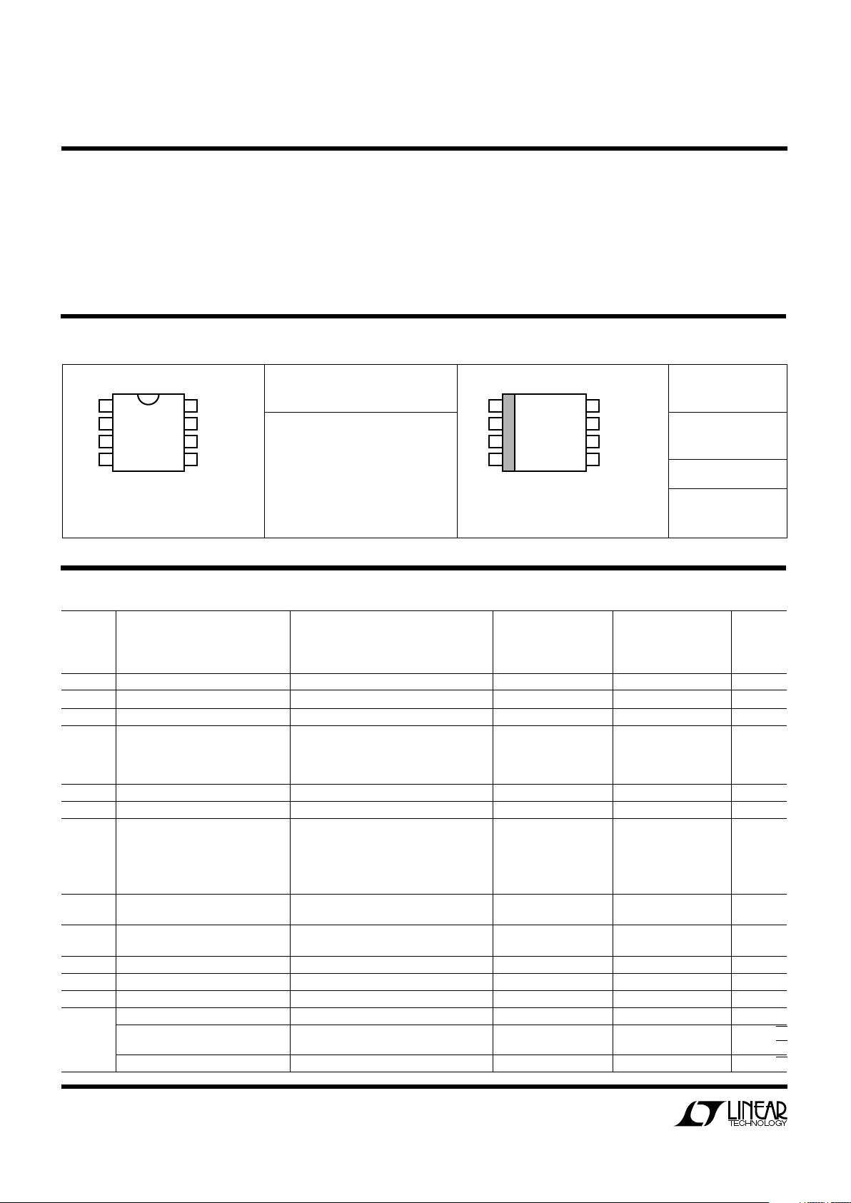
WU
U
PACKAGE
/
O
RDER I FOR ATIO
LT1122AMJ8 LT1122CCJ8
LT1122BMJ8 LT1122DCJ8
LT1122CMJ8 LT1122ACN8
LT1122DMJ8 LT1122BCN8
LT1122ACJ8 LT1122CCN8
LT1122BCJ8 LT1122DCN8
ORDER PART
NUMBER
ORDER PART
NUMBER
LT1122CS8
LT1122DS8
PART MARKING
1122C
1122D
A
U
G
W
A
WUW
ARB
S
O
LUTEXI T
I
S
8
7
6
54
3
2
1
V
TRIM
–IN
+IN
V
V TRIM
OUT
+
V
SPEED BOOST/
OVERCOMP
TOP VIEW
N8 PACKAGE
8-LEAD PLASTIC DIP
–
OS
OS
LT1122
J8 PACKAGE
8-LEAD HERMETIC DIP
T
JMAX
= 150°C, θJA = 130°C/W (N8)
T
JMAX
= 175°C, θJA = 100°C/W (J8)
8
7
6
54
3
2
1
–IN
V
TRIM
+IN
–
V TRIM
OUT
OS
V
SPEED BOOST/
OVERCOMP
TOP VIEW
S8 PACKAGE
8-LEAD PLASTIC SOIC
+
OS
V
LT1122
T
JMAX
= 150°C, θJA = 190°C/W
Consult factory for Industrial grade parts.
E
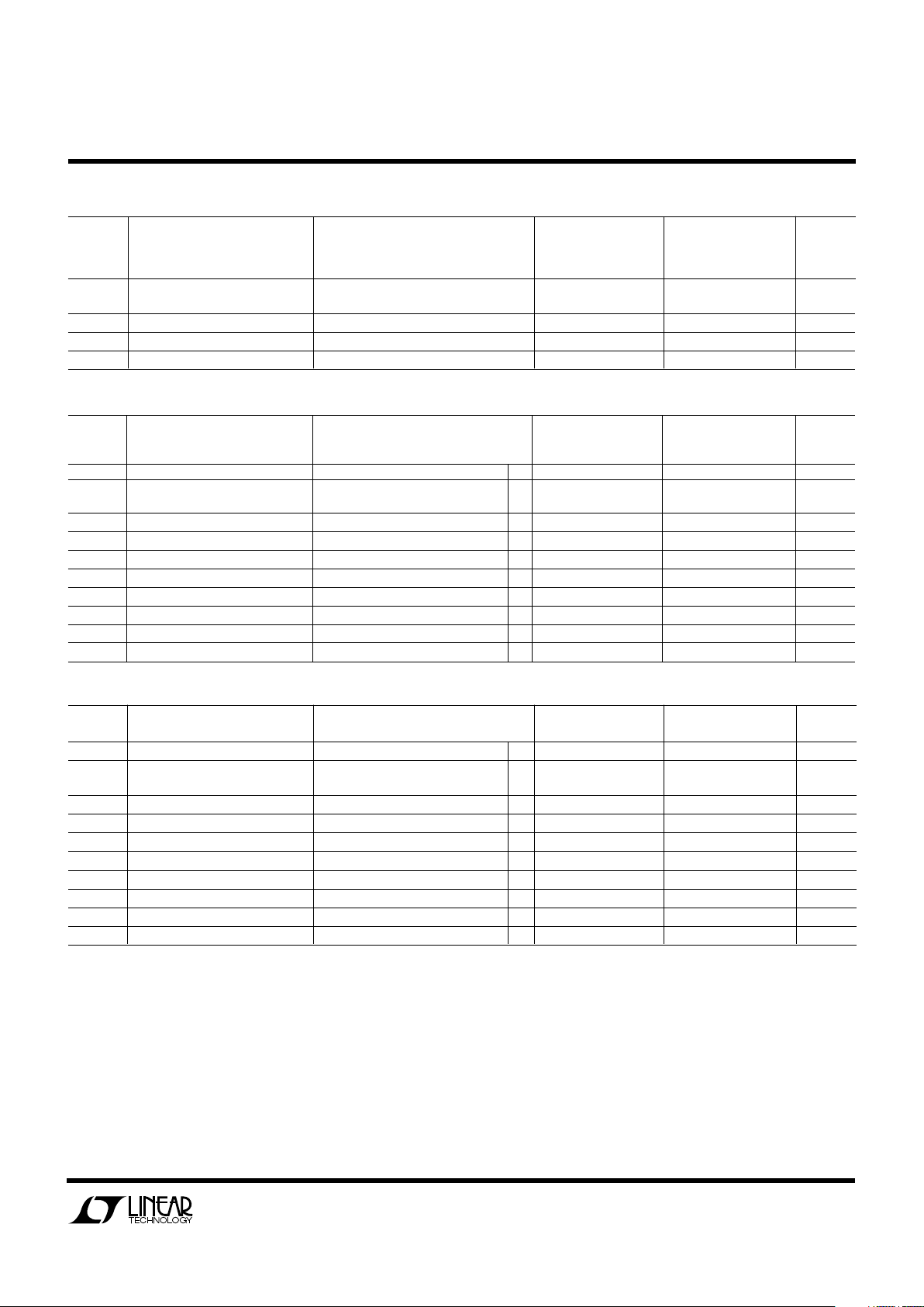
LECTRICAL C CHARA TERIST
ICS
VS = ± 15V, TA = 25°C, VCM = 0V unless otherwise noted. (Note 1)
LT1122CM/DM
LT1122AM/BM LT1122CC/DC
LT1122AC/BC LT1122CS/DS
SYMBOL PARAMETER CONDITIONS MIN TYP MAX MIN TYP MAX UNITS
V
OS
Input Offset Voltage 120 600 130 900 µV
I
OS
Input Offset Current 4 40 5 50 pA
I
B
Input Bias Current 10 75 12 100 pA
Input Resistance
Differential 10
12
10
12
Ω
Common Mode V
CM
= – 10V to + 8V 10
12
10
12
Ω
V
CM
= + 8V to + 11V 10
11
10
11
Ω
Input Capacitance 44pF
S
R
Slew Rate AV = – 1 60 80 50 75 V/µs
Settling Time (Note 2) + 10V to 0V, – 10V to 0V
100% Tested: A and C Grades
to 1mV at Sum Node 340 540 350 590 ns
B and D Grades to 1mV at Sum Node 350 360 ns
All Grades to 0.5mV at Sum Node 450 470 ns
GBW Gain Bandwidth Product 14 13 MHz
Power Bandwidth V
OUT
= 20Vp-p 1.2 1.1 MHz
A
VOL
Large Signal Voltage Gain V
OUT
= ±10V, RL = 2kΩ 180 500 150 450 V/mV
V
OUT
= ± 10V, RL = 600Ω 130 250 110 220 V/mV
CMRR Common Mode Rejection Ratio VCM = ± 10V 83 99 80 98 dB
Input Voltage Range (Note 3) ±10.5 ±11 ± 10.5 ± 11 V
PSRR Power Supply Rejection Ratio VS = ±10V to ± 18V 86 103 82 101 dB
Input Noise Voltage 0.1Hz to 10Hz 3.0 3.3 µV
P-P
Input Noise Voltage Density fO = 100Hz 25 27 nV/√Hz
fO = 10kHz 14 15 nV/√Hz
Input Noise Current Density fO = 100Hz, fO = 10kHz 2 2 fA/√Hz
Page 3
3
LT1122
E
LECTRICAL C CHARA TERIST
ICS
LT1122CM/DM
LT1122AM/BM LT1122CC/DC
LT1122AC/BC LT1122CS/DS
SYMBOL PARAMETER CONDITIONS MIN TYP MAX MIN TYP MAX UNITS
VS = ± 15V, TA = 25°C, VCM = 0V unless otherwise noted.
LT1122CC/DC
LT1122AC/BC LT1122CS/DS
SYMBOL PARAMETER CONDITIONS MIN TYP MAX MIN TYP MAX UNITS
V
OS
Input Offset Voltage • 350 1400 400 2000 µV
Average Temperature Coefficient • 518 6 25 µV/°C
of Input Offset Voltage
I
OS
Input Offset Current • 12 150 15 200 pA
I
B
Input Bias Current • 80 600 90 800 pA
A
VOL
Large Signal Voltage Gain V
OUT
= ± 10V, R
L
≥ 2kΩ • 120 380 100 340 V/mV
CMRR Common Mode Rejection Ratio V
CM
= ±10V • 82 98 78 96 dB
PSRR Power Supply Rejection Ratio V
S
= ±10V to ± 17V • 84 101 80 99 dB
Input Voltage Range • ±10 ± 10.8 ± 10 ±10.8 V
V
OUT
Output Voltage Swing R
L
= 2kΩ • ±11.5 ±12.4 ± 11.5 ± 12.4 V
S
R
Slew Rate A
V
= – 1 • 50 70 40 65 V/µs
VS = ± 15V, VCM = 0V, 0°C ≤ TA ≤ 70°C, unless otherwise noted. (Note 1)
LT1122AM/BM LT1122CM/DM
SYMBOL PARAMETER CONDITIONS MIN TYP MAX MIN TYP MAX UNITS
V
OS
Input Offset Voltage • 650 2400 800 3400 µV
Average Temperature Coefficient • 618 725 µV/°C
of Input Offset Voltage
I
OS
Input Offset Current • 0.5 6 0.6 9 nA
I
B
Input Bias Current • 625 735 nA
A
VOL
Large Signal Voltage Gain V
OUT
= ± 10V, R
L
≥ 2kΩ • 70 230 60 200 V/mV
CMRR Common Mode Rejection Ratio V
CM
= ±10V • 80 97 76 94 dB
PSRR Power Supply Rejection Ratio V
S
= ±10V to ± 17V • 83 100 78 98 dB
Input Voltage Range • ±10 ± 10.5 ± 10 ±10.5 V
V
OUT
Output Voltage Swing R
L
= 2kΩ • ±11.3 ±12.1 ± 11.3 ± 12.1 V
S
R
Slew Rate A
V
= – 1 • 45 60 35 55 V/µs
VS = ± 15V, VCM = 0V, – 55°C ≤ TA ≤ 125°C, unless otherwise noted. (Note 1)
The • denotes the specifications which apply over the full operating
temperature range.
Note 1: The LT1122 is measured in an automated tester in less than one
second after application of power. Depending on the package used, power
dissipation, heat sinking, and air flow conditions, the fully warmed up chip
temperature can be 10°C to 50°C higher than the ambient temperature.
Note 2: Settling time is 100% tested for A and C grades using the settling
time test circuit shown. This test is not included in quality assurance
sample testing.
Note 3: Input voltage range functionality is assured by testing offset
voltage at the input voltage range limits to a maximum of 4mV (A, B
grades), to 5.7mV (C, D grades).
Note 4: Minimum supply voltage is tested by measuring offset voltage to
7mV maximum at ±5V supplies.
Note 5: The LT1122 is not tested and not quality-assurance-sampled at
–40°C and at 85°C. These specifications are guaranteed by design,
correlation and/or inference from – 55°C, 0°C, 25°C, 70°C and/or 125°C
tests.
V
OUT
Output Voltage Swing RL = 2kΩ±12 ±12.5 ± 12 ± 12.5 V
RL = 600Ω±11.5 ± 12 ± 11.5 ±12 V
I
S
Supply Current 7.5 10 7.8 11 mA
Minimum Supply voltage (Note 4) ± 5 ±5V
Offset Adjustment Range R
POT
≥ 10k, Wiper to V
+
±4 ±10 ±4 ± 10 mV
Page 4

4
LT1122
VS = ± 15V, VCM = 0V, – 40°C ≤ TA ≤ 85°C, unless otherwise noted. (Note 5)
Settling Time Test Fixture
E
LECTRICAL C CHARA TERIST
ICS
LT1122CC/DC
LT1122AC/BC LT1122CS/DS
SYMBOL PARAMETER CONDITIONS MIN TYP MAX MIN TYP MAX UNITS
V
OS
Input Offset Voltage • 450 1900 500 2700 µV
Average Temperature Coefficient • 620 728 µV/°C
of Input Offset Voltage
I
OS
Input Offset Current • 30 600 40 900 pA
I
B
Input Bias Current • 230 2000 260 2700 pA
A
VOL
Large Signal Voltage Gain V
OUT
= ± 10V, R
L
≥ 2kΩ • 95 340 80 300 V/mV
CMRR Common Mode Rejection Ratio V
CM
= ±10V • 80 98 76 96 dB
PSRR Power Supply Rejection Ratio V
S
= ±10V to ± 17V • 83 100 78 98 dB
Input Voltage Range • ±10 ± 10.6 ± 10 ±10.6 V
V
OUT
Output Voltage Swing R
L
= 2kΩ • ±11.3 ±12.2 ± 11.3 ± 12.2 V
S
R
Slew Rate A
V
= – 1 • 45 65 35 60 V/µs
16
15
14
13
12
11
10
9
8
7
6
5
4
3
2
1
+15V
1 F TANTµ0.1 Fµ
1 F TANTµ0.1 Fµ
TYPICAL SUPPLY
BYPASSING FOR
EACH AMP/BUFFER
–10V
(REGULATED)
1
2
TTL
IN
4
5
74LS00
GROUND ALL
OTHER INPUTS
+10V
(REGULATED)
6
3
SETTLING
TIME OUTPUT
(20 TIMES SUM
NODE OUTPUT)
1k
NO CONNECTION ON PINS
10, 11, 12, 14, AND 15
1N5712
+15V
–15V
1.5k
LT1223
51
–
+
3
2
4
7
6
8
1
7
2
5
4
51
1N5712
SUMMING
NODE
OUTPUT
–15V
+15V
*THIS RESISTOR CAN BE ADJUSTED TO
NULL OUT ALL OFFSETS AT THE SETTLING
TIME OUTPUT. THE AUTOMATED TESTER
USES A SEPARATE AUTOZERO CIRCUIT.
–15V
(MEASURE INPUT
PULSE HERE)
V
IN
5.1k
1%
4
–15V
3
2
7
6
LT1122
+
–
2k
1%
+15V
2k
1%
DEVICE UNDER TEST
5pF
+15V
7
1
5
2
8
51
51
HA5002
79
5.1k*
1%
HA5002
4
LTC201A
LT1122•TA02
+
+
–15V
Page 5

5
LT1122
CCHARA TERIST
ICS
UW
ATYPICA
LPER
F
O
R
C
E
Settling Time Settling Time Settling Time
(Input From –10V to 0V) (Input From +10V to 0V) (Input From 0V to +10V)
100ns/DIV
1122 G01
100ns/DIV
1122 G02
100ns/DIV
1122 G03
1mV/DIV AT SUM NODE
1mV/DIV AT SUM NODE
1mV/DIV AT SUM NODE
200ns/DIV
A
V
= +1
1122 G05
Settling Time Undistorted Output Swing vs
(Input From 0V to –10V) Large Signal Response Frequency
100ns/DIV
1122 G04
1mV/DIV AT SUM NODE
5V/DIV
FREQUENCY (Hz)
100k
0
PEAK TO PEAK OUTPUT SWING (V)
10
20
25
30
1M 10M
100M
V = ±15V
T = 25°C
15
5
S
A
LT1122•TPC01
FREQUENCY (Hz)
1
0
GAIN (dB)
20
40
60
80
100
120
10 100 1k 10k
–20
–40
100k
1M 10M
100M
V = ±15V
T = 25°C
S
A
LT1122•TPC02
Common Mode Rejection vs
Voltage Gain vs Frequency Gain, Phase vs Frequency Frequency
FREQUENCY (Hz)
1M
–10
GAIN (dB)
10
20
100M
10M
0
80
100
120
140
160
180
200
V = ±15V
T = 25°C
C = 15pF
S
A
L
PHASE SHIFT (DEGREES)
LT1122•TPC03
FREQUENCY (Hz)
100
0
COMMON-MODE REJECTION RATIO (dB)
20
40
60
80
100
120
1k 10k 1M 100M
V = ±15V
T = 25°C
S
A
100k 10M
LT1122•TPC04
Page 6

6
LT1122
CCHARA TERIST
ICS
UW
ATYPICA
LPER
F
O
R
C
E
Distribution of Input Offset Input Bias and Offset Currents Bias and Offset Currents Over
Voltage Over Temperature The Common-Mode Range
CHIP TEMPERATURE (°C)
0
1
INPUT BIAS AND OFFSET CURRENTS (pA)
300
1K
3K
10K
25 50 75 100
125
100
30
10
3
BIAS
CURRENT
OFFSET
CURRENT
V = ±15V
V = 0V
S
CM
LT1122•TPC06
30K
100K
COMMON-MODE INPUT VOLTAGE (V)
–15
0
INPUT BIAS AND OFFSET CURRENT (pA)
20
40
60
80
100
120
–10 –5 5 15
V = ±15V
T = 25°C
S
A
0
10
(NOT-WARMED UP)
BIAS
CURRENT
OFFSET
CURRENT
LT1122•TPC07
Warm-up Drift Noise Spectrum 0.1Hz to 10Hz Noise
FREQUENCY (Hz)
1
10
VOLTAGE NOISE DENSITY (nV/ Hz)
100
1000
3 10 10k
30 100 300 1k
3k
V = ±15V
T = 25°C
S
A
√
LT1122•TPC09
TIME (SECONDS)
0
NOISE VOLTAGE (1 V/DIV)
24 8106
µ
LT1122•TPC10
Total Harmonic Distortion Total Harmonic Distortion Intermodulation Distortion
+ Noise vs Frequency + Noise vs Frequency (CCIF Method) vs Frequency
Inverting Gain Non-Inverting Gain LT1122 and LF156*
FREQUENCY (Hz)
20
0.0001
TOTAL HARMONIC DISTORTION + NOISE (%)
0.001
0.01
0.1
100 1k 20k
A = –50
V
A = –10
A = –1
10k
T = 25°C
V = ±15V
Z = 5k//15pF
V = 7V RMS
A
S
L
O
V
V
LT1122•TPC11
FREQUENCY (Hz)
20
0.0001
TOTAL HARMONIC DISTORTION + NOISE (%)
0.001
0.01
0.1
100 1k 20k
A = +50
V
A = +10
A = +1
10k
T = 25°C
V = ±15V
Z = 5k//15pF
V = 7V RMS
A
S
L
O
V
V
LT1122•TPC12
FREQUENCY (Hz)
3k
0.0001
INTERMODULATION DISTORTION (IMD) (%)
0.001
0.01
0.1
10k 20k
LT1122
LF156
V = ±15V
T = 25°C
A = –10
V = 7V RMS
Z = 5k//15pF
S
A
V
O
L
*SEE LT1115 DATA SHEET FOR DEFINITION
OF CCIF TESTING
LT1122•TPC13
INPUT OFFSET VOLTAGE ( V)
–900
0
NUMBER OF UNITS
200
400
600
800
–500 –100
100
500
V = ±15V
T = 25°C
(NOT WARMED UP)
S
A
3370 UNITS TESTED
IN ALL PACKAGES
µ
LT1122•TPC05
900
TIME AFTER POWER ON (MINUTES)
0
1
CHANGE IN OFFSET VOLTAGE ( V)
50
100
150
200
250
123
V = ±15V
T = 25°C
S
A
J PACKAGE
N PACKAGE
SO PACKAGE
IN STILL AIR (SO PACKAGE
SOLDERED ONTO BOARD)
LT1122•TPC08
µ
Page 7

7
LT1122
U
S
A
O
PPLICATI
WU
U
I FOR ATIO
When the feedback around the op amp is resistive (RF), a
pole will be created with RF, the source resistance and
capacitance (RS, CS), and the amplifier input capacitance
(CIN ≈ 4pF). In low closed loop gain configurations and
with RS and RF in the kilohm range, this pole can create
excess phase shift and even oscillation. A small capacitor
(CF) in parallel with RF eliminates this problem. With
RS (CS + CIN) = RFCF, the effect of the feedback pole is
completely removed.
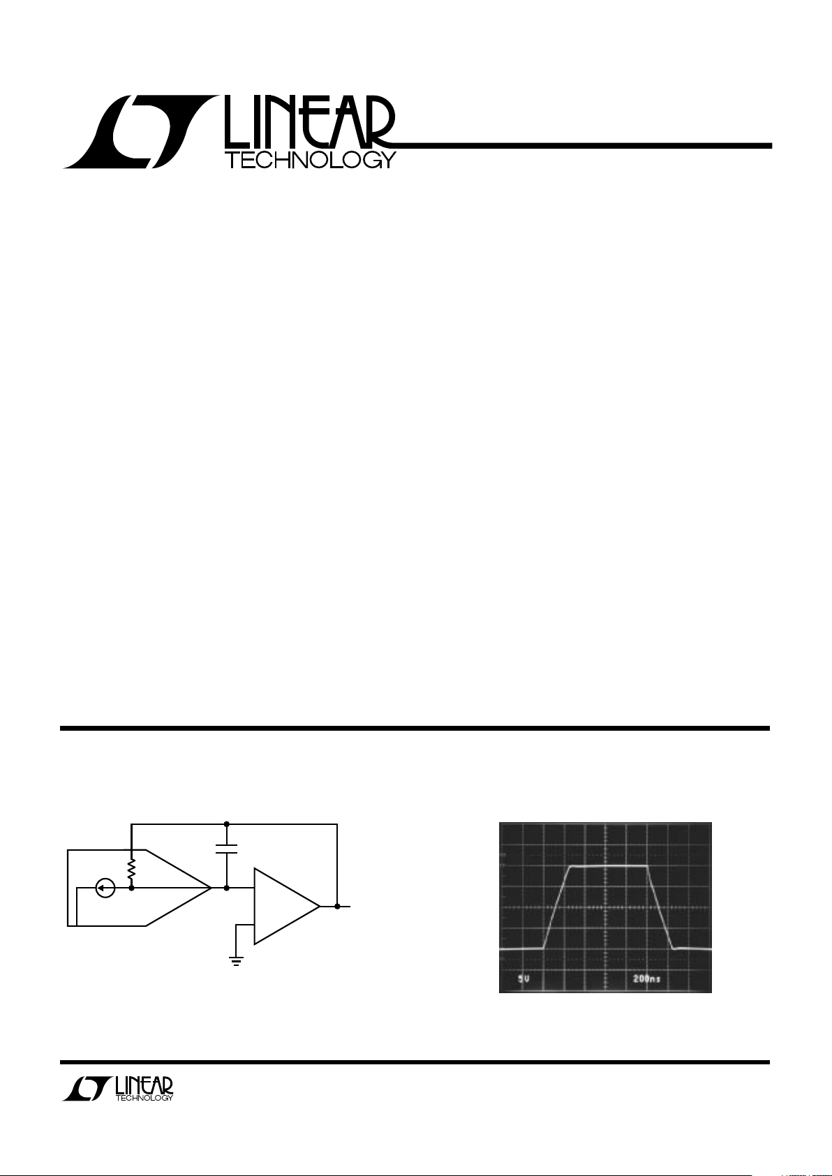
Settling Time Measurements
Settling time test circuits shown on some competitive
devices’ data sheets require:
1. A “flat top” pulse generator. Unfortunately, flat top
pulse generators are not commercially available.
2. A variable feedback capacitor around the device under
test. This capacitor varies over a four to one range.
Presumably, as each op amp is measured for settling
time, the capacitor is fine tuned to optimize settling
time for that particular device.
3. A small inductor load to optimize settling.
The LT1122’s settling time is 100% tested in the test
circuit shown. No “flat top” pulse generator is required.
The test circuit can be readily constructed, using commercially available ICs. Of course, standard high frequency
board construction techniques should be followed. All
LT1122s are measured with a constant feedback capacitor. No fine tuning is required.
Speed Boost/Overcompensation Terminal
Pin 8 of the LT1122 can be used to change the input stage
operating current of the device. Shorting pin 8 to the
positive supply (Pin 7) increases slew rate and bandwidth
by about 25%, but at the expense of a reduction in phase
margin by approximately 18 degrees. Unity gain capacitive load handling decreases from typically 500pF to
100pF.
Conversely, connecting a 15k resistor from pin 8 to
ground pulls 1mA out of pin 8 (with V+ = 15V). This
reduces slew rate and bandwidth by 25%. Phase margin
and capacitive load handling improve; the latter typically
increasing to 800pF.
High Speed Operation
As with most high speed amplifiers, care should be taken
with supply decoupling, lead dress and component
placement.
The power supply connections to the LT1122 must maintain a low impedance to ground over a bandwidth of
20MHz. This is especially important when driving a significant resistive or capacitive load, since all current delivered
to the load comes from the power supplies. Multiple high
quality bypass capacitors are recommended for each
power supply line in any critical application. A 0.1µF
ceramic and a 1µ F electrolytic capacitor, as shown, placed
as close as possible to the amplifier (with short lead
lengths to power supply common) will assure adequate
high frequency bypassing, in most applications.
R
S
C
S
C
IN
R
F
C
F
OUTPUT
+
–
LT1122•TA04
µ
V
+
7
2
6
3
4
1 F
µ0.1 F
µ1 F
µ0.1 F
+
V
–
LT1122
LT1122•TA03
+
+
–
Information furnished by Linear Technology Corporation is believed to be accurate and reliable.
However, no responsibility is assumed for its use. Linear Technology Corporation makes no representation that the interconnection of circuits as described herein will not infringe on existing patent rights.
Page 8

8
LT1122
LT1122
TYPICAL APPLICATIONS
U
Quartz Stabilized Oscillator With 9ppm Distortion
µ
Ω
DISTORTION
TRIM
50k
430pF
560k
47k
4kHz
J
CUT
LT1010LT1122
+
–
LT1122
–15V
+15V
2k
1/4 LTC201
GROUND CRYSTAL CASE
= VACTEC VTL5C10 OR
CLAIREX CLM410
= 1N4148
+15V
1M
560k
100k
Q1
2N3904
+15V
LT1122•TA05
–
+
4.7k
4.7k 5k
OUTPUT
AMPLITUDE
TRIM
+
10 F
470
LT1006
LT1004
2.5V
4.7k
–15V
OUTPUT
+
–
MOUNT IN CLOSE
PROXIMITY
PACKAGE DESCRIPTION
U
µ
IN
V
OUT
E DC
+
–
1 F
200k
1%
20k
1%
100k
1%
1k
50k
200k
1%
20k
1%
LT1122
OUTPUT DC = RMS VALUE OF INPUT
BANDWIDTH WITH 10Vp-p INPUT = 2MHz
+
–
LT1122
LT1122•TA06
Wide-Band, Filtered, Full Wave Rectifier
Please see the
1994 Linear Databook Volume III
for package descriptions.
 Loading...