

Page 1
FEATURES
LT1120
Micropower Regulator with
Comparator and Shutdown
U
DESCRIPTIO
■
40µA Supply Current
■
125mA Output Current
■
2.5V Reference Voltage
■
Reference Output Sources 2mA and Sinks 2mA
■
Open Collector
■
Comparator Sinks 10mA
■
Logic Shutdown
■
0.2V Dropout Voltage
■
Thermal Limiting
■
Available in 8-Lead DIP, SO and Metal Can Packages
U
APPLICATIO S
■
Battery Systems
■
Battery-Backup System
■
Portable Terminals
■
Portable Instruments
■
Memory Keep-Alive
U
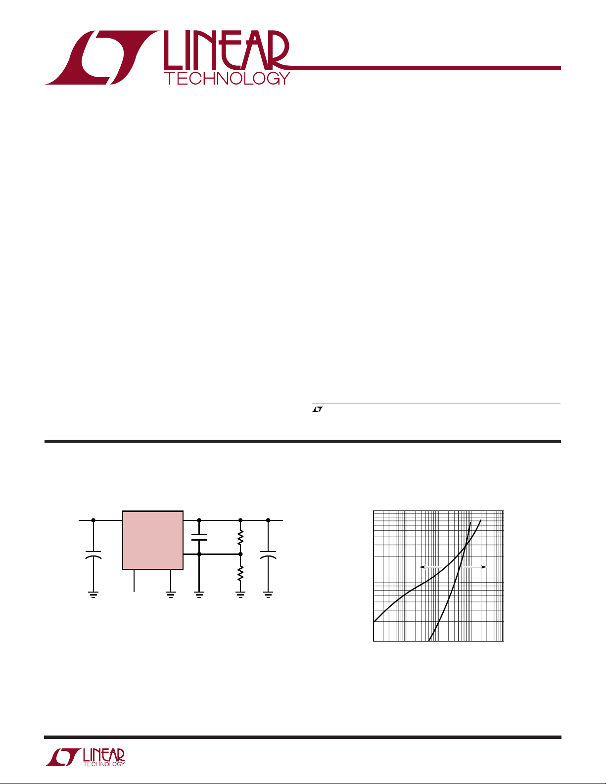
TYPICAL APPLICATIO
The LT®1120 is a combination micropower positive regulator and free collector comparator on a single monolithic
chip. With only 40µA supply current, the LT1120 can
supply over 125mA of output current. Input voltage range
is from 4.5V to 36V and dropout voltage is 0.6V at 125mA.
Dropout voltage decreases with lower load currents. Also
included on the chip is a class B output 2.5V reference that
can either source or sink current. A shutdown pin allows
logic shutdown of the output.
The comparator can be used for system or battery monitoring. For example, the comparator can be used to warn
of low system voltage. Frequency compensation of the
comparator for amplifier applications can be obtained by
adding external output capacitance.
The 2.5V reference will source or sink current. This allows
it to be used as a supply splitter or auxiliary output.
, LTC and LT are registered trademarks of Linear Technology Corporation.
V
IN
I
Q
> 5.2V
= 40µA
5V Regulator
5
V
IN
+ +
10µF
LT1120
SHUTDOWN
4
V
OUT
0.001µF1M
2
FB
GNDSHDN
13
1M
25µF
1120 TA01
Dropout Voltage and Supply Current
5V
1.00
0.10
DROPOUT VOLTAGE (V)
0.01
0.1 1
OUTPUT CURRENT (mA)
10 100 1000
10
SUPPLY CURRENT (mA)
1
0.1
1120 TA02
1
Page 2
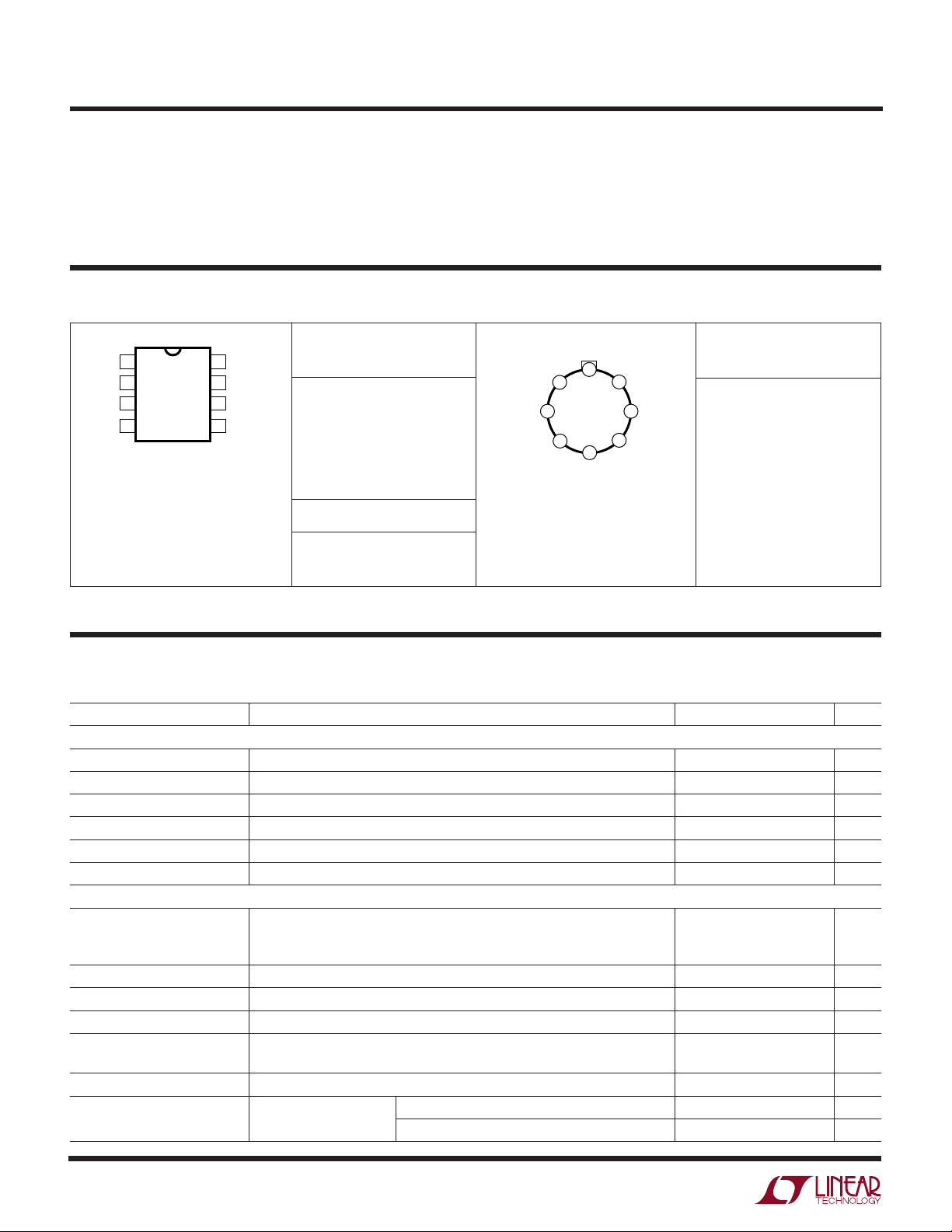
LT1120
TOP VIEW
COMPOUT
–INPUT
GND
FB REF
V
IN
SHDN
V
OUT
8
7
6
5
3
2
1
4
H PACKAGE
8-LEAD TO-5 METAL CAN
WW
W
ABSOLUTE AXI U RATI GS
U
(Note 1)
Input Voltage ........................................................... 36V
NPN Collector Voltage ............................................. 36V
Output Short-Circuit Duration.......................... Indefinite
Power Dissipation............................... Internally Limited
UUW
PACKAGE/ORDER I FOR ATIO
GND
1
FB
2
SHDN
3
V
4
OUT
J8 PACKAGE
8-LEAD CERDIP
S8 PACKAGE
8-LEAD PLASTIC SO
T
= 150°C, θJA = 100°C/W (J)
JMAX
= 110°C, θJA = 130°C/W (N)
T
JMAX
= 110°C, θJA = 150°C/W (S)
T
JMAX
TOP VIEW
N8 PACKAGE
8-LEAD PDIP
–INPUT
8
COMPOUT
7
REF
6
V
5
IN
ORDER PART
NUMBER
LT1120CJ8
LT1120CN8
LT1120CS8
LT1120IN8
LT1120IS8
S8 PART MARKING
1120
1120I
Operating Temperature Range
LT1120C................................................ 0°C to 100°C
LT1120I ................................................ –40 to 100°C
Storage Temperature Range ................. –65°C to 150°C
ORDER PART
NUMBER
LT1120CH
T
= 150°C, θJA = 150°C/W, θJC = 45°C/W
JMAX
Consult factory for Military grade parts.
ELECTRICAL CHARACTERISTICS
operating temperature range, otherwise specifications are at T
PARAMETER CONDITIONS MIN TYP MAX UNITS
Reference
Reference Voltage 4.5V ≤ VIN ≤ 36V 2.46 2.50 2.54 V
Line Regulation 4.5V ≤ VIN ≤ 36V 0.01 0.015 %/V
Load Regulation –2mA ≤ I
Output Source Current VIN = 5V 2 4 mA
Output Sink Current VIN = 5V 2 4 mA
Temperature Stability 1%
Regulator
Supply Current VIN = 6V, I
Output Current (VIN – V
Load Regulation (VIN – V
Line Regulation 6V ≤ VIN ≤ 36V 0.01 0.015 %/V
Dropout Voltage I
Feedback Sense Voltage VIN = 12V 2.44 2.5 2.56 V
Shutdown Pin Voltage Normal 0.4 V
The ● denotes the specifications which apply over the full
= 25°C. Tj = 25°C
A
≤ 2mA, VIN = 12V 0.3 0.6 %
REF
≤ 100µA4580µA
OUT
= 36V, I
V
IN
V
= 12V, I
IN
= 100µA 0.02 0.05 V
OUT
I
= 125mA 0.4 0.65 V
OUT
V
≤ 0.5V Shutdown 2.2 1.4 V
OUT
≤ 100µA 75 100 µA
OUT
= 125mA 11 20 mA
OUT
) ≥ 1V, VIN ≥ 6V 125 mA
OUT
) ≥ 1V, VIN ≥ 6V 0.2 0.5 %
OUT
2
Page 3
LT1120
ELECTRICAL CHARACTERISTICS
operating temperature range, otherwise specifications are at T
PARAMETER CONDITIONS MIN TYP MAX UNITS
Shutdown Pin Current VIN = 1.4V 25 µA
Feedback Bias Current 15 40 nA
Minimum Load Current VIN = 36V 15 µA
Short-Circuit Current VIN = 36V 300 400 mA
Comparator
Offset Voltage VIN = 36V 37mV
Bias Current VIN = 36V (Note 2) 15 40 nA
Gain ∆V
Power Supply Rejection 4.5V ≤ VS ≤ 36V 80 96 dB
Output Sink Current VIN = 4.5V 10 18 mA
Saturation Voltage I
Input Voltage Range 0V
Response Time 5 µs
Leakage Current 2 µA
= 29V, RL = 20k 2000 10000 V/V
OUT
= 1mA 0.4 0.6 V
OUT
The ● denotes the specifications which apply over the full
= 25°C. Tj = 25°C
A
– 1 V
IN
ELECTRICAL CHARACTERISTICS
The ● denotes the specifications which apply over the full operating temperature range, otherwise specifications are at TA = 25°C.
PARAMETER CONDITIONS MIN TYP MAX UNITS
Reference
Reference Voltage 4.5V ≤ VIN ≤ 36V ● 2.40 2.50 2.55 V
Line Regulation 4.5V ≤ VIN ≤ 36V ● 0.01 0.02 %/V
Load Regulation –2mA ≤ I
Output Source Current VIN = 5V ● 2mA
Output Sink Current VIN = 5V ● 2mA
Regulator
Supply Current VIN = 6V, I
= 36V, I
V
IN
V
= 12V, I
IN
Output Current (VIN – V
Load Regulation (VIN – V
Line Regulation 6V ≤ VIN ≤ 36V ● 0.02 %/V
Dropout Voltage I
Feedback Sense Voltage VIN = 12V ● 2.38 2.5 2.57 V
Feedback Bias Current ● 50 nA
Minimum Load Current VIN = 36V ● 50 µA
Short-Circuit Current VIN = 36V ● 300 400 mA
OUT
I
OUT
≤ 2mA, VIN = 12V ● 0.4 0.8 %
REF
≤ 100µA ● 65 95 µA
OUT
≤ 100µA ● 85 100 µA
OUT
= 125mA ● 11 20 mA
OUT
) ≥ 1V, VIN ≥ 6V ● 125 mA
OUT
) ≥ 1V, VIN ≥ 6V ● 1%
OUT
= 100µA ● 0.06 V
= 125mA ● 0.85 V
3
Page 4
LT1120
ELECTRICAL CHARACTERISTICS
The ● denotes the specifications which apply over the full operating temperature range, otherwise specifications are at TA = 25°C.
PARAMETER CONDITIONS MIN TYP MAX UNITS
Comparator
Offset Voltage ● 10 mV
Bias Current VIN = 36V (Note 2) ● 15 60 nA
Gain ∆V
Output Sink Current VIN = 4.5V (Note 3) ● 510 mA
Leakage Current VIN = 36V ● 8 µA
= 29V, RL = 20k ● 1000 V/V
OUT
Note 1: Absolute Maximum Ratings are those values beyond which the life
a device may be impaired.
Note 2: TA > 85°C, I bias maximum is 100nA.
Note 3: For TA ≤ –40°C output current sink drops to 2.5mA.
UW
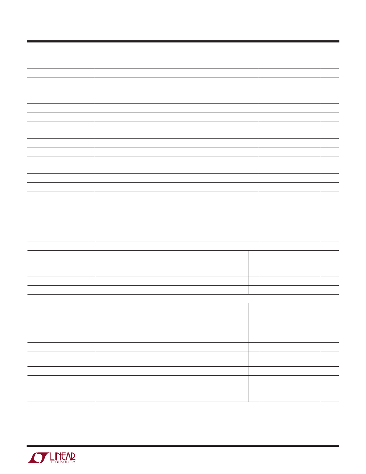
TYPICAL PERFOR A CE CHARACTERISTICS
Regulator Load Regulation Supply Current Regulator Short-Circuit Current
0.3
0.2
0.1
0
–0.1
OUTPUT VOLTAGE CHANGE (%)
–0.2
PRELOAD = 100µA
–0.3
0.1 10 100 1000
TJ = –55°C
TJ = 25°C
TJ = 125°C
1
OUTPUT CURRENT (mA)
1120 G01
100
TJ = –55°C TO 125°C
10
1
SUPPLY CURRENT (mA)
0.1
0.01
0.1 1
REGULATOR OUTPUT CURRENT (mA)
10 100 1000
1120 G02
350
300
250
200
150
100
SHORT-CIRCUIT CURRENT (mA)
CURRENT LIMIT TIED TO GROUND
50
0
–50 –10 30 70 110 150
TEMPERATURE (°C)
1120 G03
Dropout Voltage
1
∆V
= 100mV
OUT
0.1
REGULATOR INPUT-OUTPUT DIFFERENTIAL (V)
0.01
0.1 1
REGULATOR OUTPUT CURRENT (mA)
10 100 1000
4
1120 G04
Regulator Minimum Load Current Regulator Ripple Rejection
100
10
MINIMUM LOAD CURRENT (µA)
1
70 80 90 100 110 120 130 140 150
TEMPERATURE (°C)
1120 G05
70
65
60
55
I
= 10mA
OUT
50
45
RIPPLE REJECTION (dB)
40
35
30
10 1k 10k 100k
I
= 1mA
OUT
VIN = 10VDC, 1V
V
= 5V
OUT
= 10µF
C
OUT
100
RIPPLE FREQUENCY (Hz)
P–P
I
OUT
= 100mA
1120 G06
Page 5

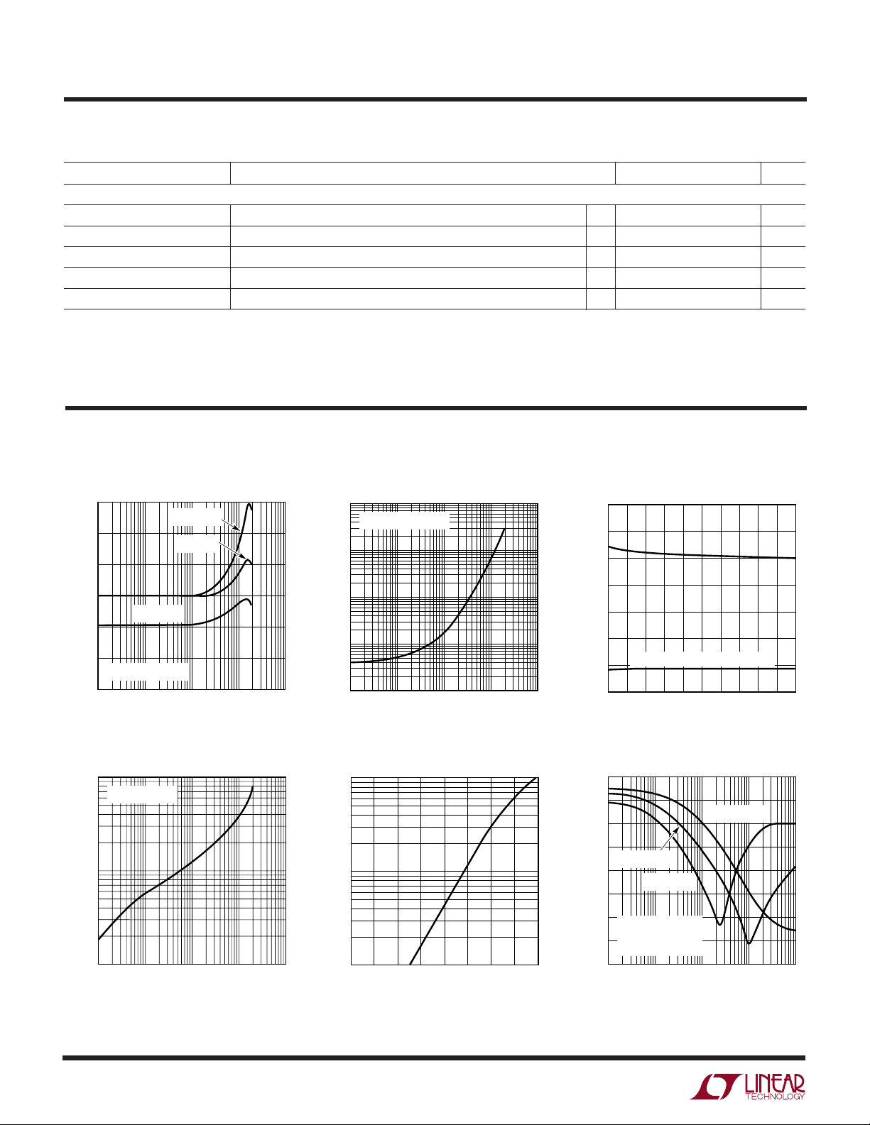
UW
INPUT VOLTAGE (V)
012345678
OUTPUT VOLTAGE (V)
1120 G13
5.5
5.0
4.5
4.0
3.5
3.0
2.5
2.0
0
V
OUT
= 5V
RL = 50Ω
RL = 500Ω
NO LOAD
TYPICAL PERFOR A CE CHARACTERISTICS
LT1120
Supply Current
10
I
= 100mA
OUT
1
I
= 10mA
OUT
0.1
I
= 1mA
OUT
SUPPLY CURRENT (mA)
V
= 5V
OUT
= –55°C TO 125°C
T
J
0.01
1 5 10 15 20 25
REGULATOR INPUT-OUTPUT DIFFERENTIAL (V)
Reference Regulation
4
3
2
1
0
–1
–2
–3
REFERENCE VOLTAGE CHANGE (mV)
–4
–1.5 –1.0 –0.5 0 0.5 1.0 1.5
REFERENCE OUTPUT CURRENT (mA)
1120 G07
1120 G09
Supply Current at Dropout
10
TJ = –55°C TO 125°C
1
0.1
SUPPLY CURRENT (mA)
0.01
1 0.1 0.2 0.3 0.4 0.5 0.6
REGULATOR INPUT-OUTPUT DIFFERENTIAL (V)
I
I
I
OUT
OUT
OUT
= 100mA
= 10mA
= 1mA
Feedback Pin Current
40
35
30
25
20
15
10
FEEDBACK CURRENT (nA)
5
0
0.1 10 100 1000
1
REGULATOR OUTPUT CURRENT (mA)
TJ = –55°C
TJ = 25°C
TJ = 125°C
1120 G08
1120 G11
Regulator Thermal Regulation
0.1
0
CHANGE (%)
OUTPUT VOLTAGE
–0.1
OUTPUT
50
0
CURRENT (mA)
VIN = 15V
= 5V
V
OUT
0 20 40 60 80 100 120 140 160 180
TIME (ms)
1120 G12
LT1120 Turn-On Characteristic
5
Page 6

LT1120
UUU
PI FU CTIO S
GND (Pin 1): Ground.
FB (Pin 2): Feedback. This is the feedback point of the
regulator. When operating, it is nominally at 2.5V. Optimum source resistance is 200k to 500k. The feedback pin
should not be driven below ground or more positive than
5V.
SHDN (Pin 3): Shutdown. A logic 1 shuts off the main
regulator. Caution: noise or leakage into the shutdown pin
can affect output voltage.
V
(Pin 4): Regulator Output. Main output, requires a
OUT
10µF output capacitor. Can be shorted to VIN or ground
without damaging the device.
W
BLOCK DIAGRA
REF
6
5V
IN
V
(Pin 5): Input Supply. Bypass with a 10µF capacitor.
IN
Must always be more positive than ground.
REF (Pin 6): Reference. 2.5V can source or sink current.
May be shorted to ground or up to 5V. Voltages in excess
of 5V can damage the device.
COMPOUT (Pin 7): Comparator Output. May be connected to any voltage from ground to 36V more positive
than ground (operates above VIN). Short-circuit protected.
– INPUT (Pin 8): Comparator Input. Inverting comparator
input.
7COMPOUT
U
+
–
8
–INPUT
WUU
REF
2.5V
50k
APPLICATIO S I FOR ATIO
The LT1120 is especially suited for micropower system
applications. For example, the comparator section of the
LT1120 may be used as a battery checker to provide an
indication of low battery. Another type of system application for the LT1120 would be to generate the equivalent of
split supplies off of a single power input. The regulator
section provides regulated output voltage and the reference, which can both source and sink current, is then an
artificial system ground providing a split supply for the
system.
4
V
OUT
2FB
60k
3 SHDN
1 GND
1120 BD
For many applications the comparator can be frequency
compensated to operate as an amplifier. Compensation
values for various gains are given in the data sheet. The
comparator gain is purposely low to make it easier to
frequency compensate as an amplifier. The NPN output is
capable of sinking 10mA and can drive loads connected to
voltages in excess of the positive power supply. This is
useful for driving switches or linear regulators off of a
higher input voltage.
6
Page 7

LT1120
U
WUU
APPLICATIO S I FOR ATIO
Reference
Internal to the LT1120 is a 2.5V trimmed class B output
reference. The reference was designed to be able to source
or sink current so it could be used in supply splitting
applications as well as a general purpose reference for
external circuitry. The design of the reference allows it to
source typically 4mA or 5mA and sink 2mA. The available
source and sink current decreases as temperature increases. It is sometimes desirable to decrease the AC
output impedance by placing an output capacitor on them.
The reference in the LT1120 becomes unstable with large
capacitive loads placed directly on it. When using an
output capacitor, about 20Ω should be used to isolate the
capacitor from the reference pin. This 20Ω resistor can be
placed directly in series with the capacitor or alternatively
the reference line can have 20Ω placed in series with it and
then a capacitor to ground. This is shown in Figure 1. Other
than placing large capacitive loads on the reference, no
other precautions are necessary and the reference is
stable with nominal stray capacitances.
Overload Protection
The main regulator in the LT1120 is current limited at
approximately 250mA. The current limit is stable with both
input voltage and temperature.
Like most other IC regulators, a minimum load is required
on the output of the LT1120 to maintain regulation. For
most standard regulators this is normally specified at
5mA. Of course, for a micropower regulator this would be
a tremendously large current. The output must be large
enough to absorb all the leakage current of the pass
transistor at the maximum operating temperature. It also
effects the transient response; low output currents have
long recovery times from load transients. At high operating temperatures the minimum load current increases and
having too low of a load current may cause the output to
go unregulated. Devices are tested for minimum load
current at high temperature. The output voltage setting
resistors to the feedback terminal can usually be used to
provide the minimum load current.
REF
6
OUTPUT
20Ω
+
10µF
Figure 1. Bypassing Reference
OR
REF
6
20Ω
+
10µF
OUTPUT
1120 F01
Frequency Compensation
The LT1120 is frequency compensated by a dominant pole
on the output. An output capacitor of 10µF is usually large
enough to provide good stability. Increasing the output
capacitor above 10µF further improves stability. In order
to ensure stability, a feedback capacitor is needed between
the output pin and the feedback pin. This is because stray
capacitance can form another pole with the large value of
feedback resistors used with the LT1120. Also, a feedback
capacitor minimizes noise pickup and improves ripple
rejection.
With the large dynamic operating range of the output
current, 10000:1, frequency response changes widely.
Low AC impedance capacitors are needed to insure stability. While solid tantalum are best, aluminum electrolytics
can be used but larger capacitor values may be needed.
7
Page 8

LT1120
U
TYPICAL APPLICATIO S
Regulator with Output Voltage Monitor
5V
LT1120
LOGIC
OUTPUT
500k
7
DROPS BY 100mV
OUT
LOGIC
LOGIC OUTPUT GOES LOW WHEN V
Compensating the Comparator as an Op Amp
50
6
+
8
–
R2
Av R1 C1 C2 R2
133Ω 0.1µF 0.001µF—
10 100Ω 0.047µF — 100k
100 10k 0.002µF — 10k
7
1M
C2
µA
AT Av = 100,
SLEW RATE = +0.05V/µs
R1
C1
–6V/µs
1120 TA04
5
V
IN
4
V
OUT
0.001µF 98k
V
OUT
5V
–
–INPUT 8
+
2
FB
GNDREF
16
2k
100k
+
10µF
1120 TA03
1A Low Dropout Regulator
V
IN
2.2k
10k*
MJE2955
100k150Ω*
V
OUT
5V
0.001µF100k
+
220µF
1120 TA05
†
5
V
IN
V
OUT
LT1120
FB
GND
1
* FOR CURRENT LIMIT ≈ 1.5A
†
MUST HAVE LOW ESR. SEVERAL 100µF CAPACITORS CAN BE PARALLELED.
*
4
2
8
Page 9

U
TYPICAL APPLICATIO S
LT1120
V
IN
I
Q
> 5.2V
= 40µA
5V Regulator
5
V
IN
+ +
10µF
LT1120
GND
1
4
V
OUT
0.001µF1M
2
FB
1M
Battery-Backup Regulator
BATTERY
INPUT
5
V
IN
LT1120
GND
1
4
V
OUT
2
FB
5V
25µF
1120 TA06
0.001µF1M
50k
Regulator with Improved Transient Response
5
> 5.2V
IN
V
OUT
5V
+
10µF
V
IN
LT1120
GND
1
4
V
OUT
LT1120
2
FB
GND
1
4
V
OUT
0.001µF
2
FB
5
V
IN
MAIN
POWER
INPUT
0.001µF
22k
5VV
1M
+
25µF
1M
1120 TA07
INTERNAL PARASITIC
DIODES OF LT1120
V
IN
V
IN
I
Q
* TRANSISTOR USED BECAUSE OF LOW LEAKAGE CHARACTERISTICS.
TO TURN OFF THE OUTPUT OF THE LT1120 FORCE FB (PIN 2) > 2.5V.
1M
V
OUT
5V Regulator with Feedback Shutdown
> 5.2V
= 40µA
5
V
IN
LT1120
GND
1
4
V
OUT
0.001µF1M
2
FB
1M
2N3904*
NC
1120 TA08
5V
OUT
+
10µF
LOGIC
INPUT
1120 TA09
9
Page 10

LT1120
Q35
8
Q61
Q62
Q63
Q32
Q34
Q60
Q13
Q22
Q19
Q9
Q6
Q11
Q8
Q59
–INPUT
3
SHDN
1
GND
1120 Schem
4
V
OUT
6
REF
2
FB
5
V
IN
7
COMPOUT
R17
100Ω
R10
75k
R34
60k
R38
20k
R14
15k
R15
80k
R19
40k
R8
40k
281k15k
R27
15k
R26
15k
R29
5Ω
R32
2k
R28
2k
Q30
Q21
Q24
Q31
R11
15k
Q23
Q20
Q26
Q25
R35
42k
R4
42k
Q14
Q38
Q39
Q27
C2
25pF
Q28
R18
15k
Q40
Q41
Q33
R16
6k
C3
10pF
C5
100pF
R7
6.8k
C1
10pF
Q29
Q36
Q16Q15
Q18Q17
R6
3k
R3
50k
R37
110.8k
R2
50k
R36
60k
Q5
R1
25Ω
Q2
Q10
Q12Q7
Q37
Q45 Q48
Q46 Q47
R8
100k
R30
2k
Q42
Q52
Q54
R22
30k
Q51
Q58
Q55
Q43
Q44
R24
390k
R23
30k
125k
125k
100pF
R31
10Ω
100pF
C6
100pF
Q49
Q56
R33
47k
138.3k
WW
SCHE ATIC DIAGRA
10
Page 11

PACKAGE DESCRIPTIO
LT1120
U
Dimensions in inches (millimeters) unless otherwise noted.
H Package
8-Lead TO-5 Metal Can (0.200 PCD)
(LTC DWG # 05-08-1320)
0.040
(1.016)
MAX
SEATING
PLANE
0.010 – 0.045*
(0.254 – 1.143)
0.300 BSC
(0.762 BSC)
0.008 – 0.018
(0.203 – 0.457)
NOTE: LEAD DIMENSIONS APPLY
TO SOLDER DIP/PLATE
OR TIN PLATE LEADS
0.335 – 0.370
(8.509 – 9.398)
DIA
0.305 – 0.335
(7.747 – 8.509)
0.016 – 0.021**
(0.406 – 0.533)
0° – 15°
0.045 – 0.068
(1.143 – 1.727)
0.014 – 0.026
(0.360 – 0.660)
0.050
(1.270)
MAX
45°TYP
0.028 – 0.034
(0.711 – 0.864)
0.165 – 0.185
GAUGE
PLANE
(4.191 – 4.699)
0.500 – 0.750
(12.700 – 19.050)
REFERENCE
PLANE
0.110 – 0.160
(2.794 – 4.064)
INSULATING
STANDOFF
J8 Package
8-Lead CERDIP (Narrow 0.300, Hermetic)
(LTC DWG # 05-08-1110)
MIN
0.005
(0.127)
MIN
0.025
(0.635)
RAD TYP
0.015 – 0.060
(0.381 – 1.524)
0.100 ± 0.010
(2.540 ± 0.254)
0.200
(5.080)
MAX
0.125
3.175
0.405
(10.287)
MAX
87
12
0.027 – 0.045
(0.686 – 1.143)
PIN 1
0.200
(5.080)
TYP
*
LEAD DIAMETER IS UNCONTROLLED BETWEEN THE REFERENCE PLANE
AND 0.045" BELOW THE REFERENCE PLANE
**
FOR SOLDER DIP LEAD FINISH, LEAD DIAMETER IS
65
0.220 – 0.310
(5.588 – 7.874)
0.045 – 0.068
3
4
(1.143 – 1.727)
FULL LEAD
OPTION
CORNER LEADS OPTION
0.016 – 0.024
(0.406 – 0.610)
(4 PLCS)
H8(TO-5) 0.200 PCD 1197
0.023 – 0.045
(0.584 – 1.143)
HALF LEAD
OPTION
J8 1197
N8 Package
8-Lead PDIP (Narrow 0.300)
(LTC DWG # 05-08-1510)
0.300 – 0.325
(7.620 – 8.255)
0.065
(1.651)
0.009 – 0.015
(0.229 – 0.381)
+0.035
0.325
–0.015
+0.889
8.255
()
–0.381
*THESE DIMENSIONS DO NOT INCLUDE MOLD FLASH OR PROTRUSIONS.
MOLD FLASH OR PROTRUSIONS SHALL NOT EXCEED 0.010 INCH (0.254mm)
TYP
Information furnished by Linear Technology Corporation is believed to be accurate and reliable.
However, no responsibility is assumed for its use. Linear Technology Corporation makes no representation that the interconnection of its circuits as described herein will not infringe on existing patent rights.
0.045 – 0.065
(1.143 – 1.651)
0.100 ± 0.010
(2.540 ± 0.254)
0.130 ± 0.005
(3.302 ± 0.127)
0.125
(3.175)
MIN
0.018 ± 0.003
(0.457 ± 0.076)
0.020
(0.508)
MIN
0.255 ± 0.015*
(6.477 ± 0.381)
0.400*
(10.160)
MAX
876
1234
5
N8 1197
11
Page 12

LT1120
TYPICAL APPLICATIO
U
LT1120
GND
2.2k
5
V
1
Current Limited 1A Regulator
IN
V
4
OUT
0.22µF 100k
2
FB
MJE2955
100k270Ω
0.5Ω*
V
2N3906*
+
IN
220µF
V
OUT
5V
AT 1A
†
* SETS CURRENT LIMIT BUT INCREASES DROPOUT VOLTAGE BY 0.5V.
†
MUST HAVE LOW ESR. SEVERAL 100µF CAPACITORS CAN BE PARALLELED.
PACKAGE DESCRIPTIO
0.010 – 0.020
(0.254 – 0.508)
0.008 – 0.010
(0.203 – 0.254)
*
DIMENSION DOES NOT INCLUDE MOLD FLASH. MOLD FLASH
SHALL NOT EXCEED 0.006" (0.152mm) PER SIDE
**
DIMENSION DOES NOT INCLUDE INTERLEAD FLASH. INTERLEAD
FLASH SHALL NOT EXCEED 0.010" (0.254mm) PER SIDE
× 45°
0°– 8° TYP
0.016 – 0.050
0.406 – 1.270
1120 TA10
U
Dimensions in inches (millimeters) unless otherwise noted.
S8 Package
8-Lead Plastic Small Outline (Narrow 0.150)
(LTC DWG # 05-08-1610)
0.053 – 0.069
(1.346 – 1.752)
0.014 – 0.019
(0.355 – 0.483)
0.004 – 0.010
(0.101 – 0.254)
0.050
(1.270)
TYP
0.228 – 0.244
(5.791 – 6.197)
8
1
0.189 – 0.197*
(4.801 – 5.004)
7
6
3
2
5
0.150 – 0.157**
(3.810 – 3.988)
SO8 0996
4
RELATED PARTS
PART NUMBER DESCRIPTION COMMENTS
LT1121 150mA Micropower Low Dropout Regulator 0.4V Dropout Voltage, Includes Shutdown
LT1521 300mA Mircopower Low Dropout Regulator Lowest IQ Low Dropout Regulator
LT1761 Micropower Low Noise, Low Dropout Regulator SOT-23, 20µV
Linear Technology Corporation
12
1630 McCarthy Blvd., Milpitas, CA 95035-7417
(408) 432-1900 ● FAX: (408) 434-0507
●
www.linear-tech.com
Noise, 20µA I
RMS
1120b LT/TP 0499 2K REV B • PRINTED IN USA
LINEAR TECHNOLOGY CORPORATION 1989
Q
 Loading...