

Page 1
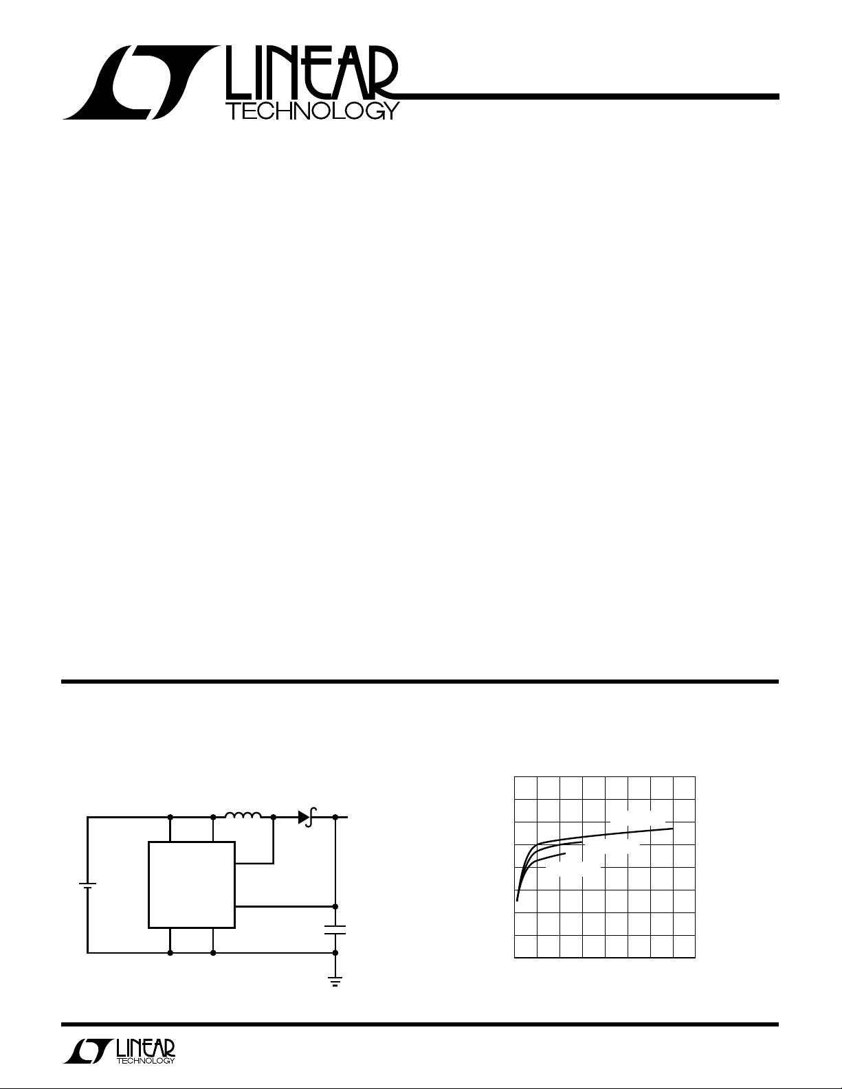
L T1110
LOAD CURRENT (mA)
0
EFFICIENCY (%)
50
60
70
80
85
90
10 20 30 40
LT1110 • TA02
75
65
55
5152535
V
IN
= 1.50V
VIN = 1.25V
VIN = 1.00V
Micropower
DC-DC Converter
Adjustable and Fixed 5V, 12V
EATU
F
■
Operates at Supply Voltages From 1.0V to 30V
■
Works in Step-Up or Step-Down Mode
■
Only Three External Off-the-Shelf Components
RE
S
Required
■
Low-Battery Detector Comparator On-Chip
■
User-Adjustable Current Limit
■
Internal 1A Power Switch
■
Fixed or Adjustable Output Voltage Versions
■
Space-Saving 8-Pin MiniDIP or S8 Package
U
O
PPLICATI
A
■
Pagers
■
Cameras
■
Single-Cell to 5V Converters
■
Battery Backup Supplies
■
Laptop and Palmtop Computers
■
Cellular Telephones
■
Portable Instruments
■
Laser Diode Drivers
■
Hand-Held Inventory Computers
S
DUESCRIPTIO
The LT1110 is a versatile micropower DC-DC converter.
The device requires only three external components to
deliver a fixed output of 5V or 12V. The very low minimum
supply voltage of 1.0V allows the use of the LT1110 in
applications where the primary power source is a single
cell. An on-chip auxiliary gain block can function as a low
battery detector or linear post regulator.
The 70kHz oscillator allows the use of surface mount
inductors and capacitors in many applications. Quiescent
current is just 300µA, making the device ideal in remote or
battery powered applications where current consumption
must be kept to a minimum.
The device can easily be configured as a step-up or
step-down converter, although for most step-down
applications or input sources greater than 3V, the LT1111
is recommended. Switch current limiting is user-adjustable
by adding a single external resistor. Unique reverse battery
protection circuitry limits reverse current to safe, nondestructive levels at reverse supply voltages up to 1.6V.
A
PPLICATITYPICAL
All Surface Mount
Single Cell to 5V Converter
SUMIDA
CD54-470K
47µH
1
I
LIM
1.5V
AA CELL*
OPERATES WITH CELL VOLTAGE 1.0V
*ADD 10 F DECOUPLING CAPACITOR IF BATTERY
µ
IS MORE THAN 2" AWAY FROM LT1110.
LT1110-5
GND SW2
54
V
SENSE
IN
2
SW1
≥
3
8
U
O
MBRS120T3
+
5V
15µF
TANTALUM
LT1110 • TA01
Efficiency
1
Page 2
LT1110
WU
U
PACKAGE
/
O
RDER I FOR ATIO
A
W
O
LUTEXI T
S
A
WUW
ARB
U
G
I
S
Supply Voltage, Step-Up Mode................................ 15V
Supply Voltage, Step-Down Mode ........................... 36V
SW1 Pin Voltage...................................................... 50V
SW2 Pin Voltage.........................................– 0.5V to V
Feedback Pin Voltage (LT1110) .............................. 5.5V
Switch Current........................................................ 1.5A
Maximum Power Dissipation ............................. 500mW
Operating Temperature Range .....................0°C to 70°C
Storage Temperature Range ..................–65°C to 150°C
Lead Temperature (Soldering, 10 sec.).................300°C
TOP VIEW
I
1
LIM
V
2
IN
Consult factory for Industrial and Military grade parts.
IN
SW1
3
SW2
4
N8 PACKAGE
8-LEAD PLASTIC DIP
*FIXED VERSIONS
T
= 90°C, θJA = 130°C/W
JMAX
I
1
LIM
V
2
IN
SW1
3
SW2
4
S8 PACKAGE
8-LEAD PLASTIC SOIC
*FIXED VERSIONS
T
= 90°C, θJA = 150°C/W
JMAX
TOP VIEW
FB (SENSE)*
8
SET
7
A0
6
GND
5
FB (SENSE)*
8
SET
7
A0
6
GND
5
ORDER PART
NUMBER
LT1110CN8
LT1110CN8-5
LT1110CN8-12
LT1110CS8
LT1110CS8-5
LT1110CS8-12
S8 PART MARKING
1110
11105
11012
LECTRICAL C CHARA TERIST
E
SYMBOL PARAMETER CONDITIONS MIN TYP MAX UNITS
I
Q
V
IN
V
OUT
f
OSC
DC Duty Cycle Full Load (VFB < V
t
ON
I
FB
I
SET
V
AO
Quiescent Current Switch Off ● 300 µA
Input Voltage Step-Up Mode ● 1.15 12.6 V
Step-Down Mode ● 30 V
Comparator Trip Point Voltage LT1110 (Note 1) ● 210 220 230 mV
Output Sense Voltage LT1110-5 (Note 2) ● 4.75 5.00 5.25 V
LT1110-12 (Note 2) ● 11.4 12.00 12.6 V
Comparator Hysteresis LT1110 ● 48 mV
Output Hysteresis LT1110-5 ● 90 180 mV
LT1110-12 ● 200 400 mV
Oscillator Frequency ● 52 70 90 kHz
Switch ON Time ● 7.5 10 12.5 µs
Feedback Pin Bias Current LT1110, VFB = 0V ● 70 150 nA
Set Pin Bias Current V
AO Output Low I
Reference Line Regulation 1.0V ≤ VIN ≤ 1.5V ● 0.35 1.0 %/V
AO
1.5V ≤ VIN ≤ 12V ● 0.05 0.1 %/V
ICS
= V
SET
REF
= –300µA, V
TA = 25°C, VIN = 1.5V, unless otherwise noted.
1.0 12.6 V
) ● 62 69 78 %
REF
● 100 300 nA
= 150mV ● 0.15 0.4 V
SET
2
Page 3
L T1110
LECTRICAL C CHARA TERIST
E
SYMBOL PARAMETER CONDITIONS MIN TYP MAX UNITS
V
CESAT
A
V
I
REV
I
LIM
I
LEAK
V
SW2
The ● denotes the specifications which apply over the full operating
temperature range.
Note 1: This specification guarantees that both the high and low trip point
of the comparator fall within the 210mV to 230mV range.
Note 2: This specification guarantees that the output voltage of the fixed
versions will always fall within the specified range. The waveform at the
sense pin will exhibit a sawtooth shape due to the comparator hysteresis.
Switch Saturation Voltage VIN = 1.5V, ISW = 400mA 300 400 mV
Step-Up Mode ● 600 mV
VIN = 1.5V, ISW = 500mA 400 550 mV
VIN = 5V, ISW = 1A 700 1000 mV
A2 Error Amp Gain RL = 100kΩ (Note 3) ● 1000 5000 V/V
Reverse Battery Current (Note 4) 750 mA
Current Limit 220Ω Between I
Current Limit Temperature – 0.3 %/°C
Coefficient
Switch OFF Leakage Current Measured at SW1 Pin 1 10 µA
Maximum Excursion Below GND I
SW1
TA = 25°C, V
ICS
LIM
≤ 10µA, Switch Off – 400 – 350 mV
= 1.5V, unless otherwise noted.
IN
● 750 mV
and V
IN
Note 3: 100kΩ resistor connected between a 5V source and the AO pin.
Note 4: The LT1110 is guaranteed to withstand continuous application of
+1.6V applied to the GND and SW2 pins while VIN, I
grounded.
400 mA
, and SW1 pins are
LIM
UW
Y
PICA
100
90
80
70
60
OSCILLATOR FREQUENCY (KHz)
50
40
LPER
F
O
R
AT
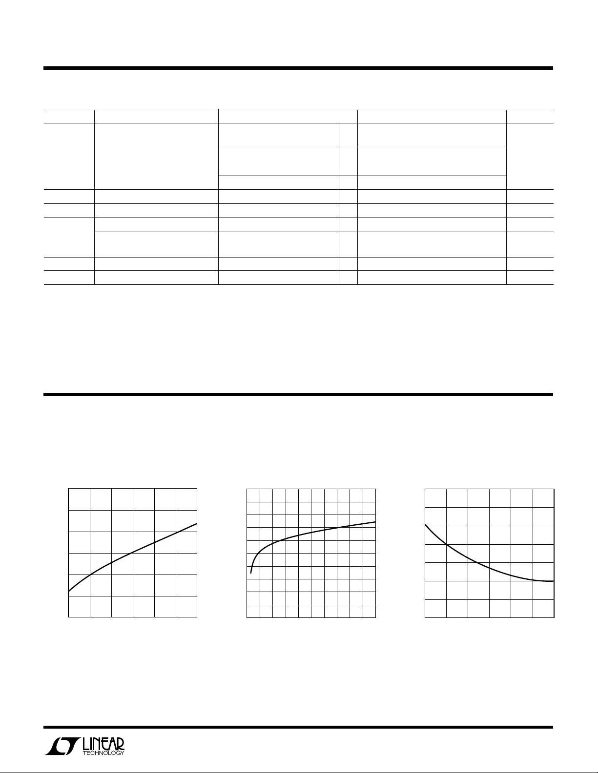
Oscillator Frequency Oscillator Frequency Switch On Time
–50
–25 0
TEMPERATURE (°C)
25
50
75
LT1110 • TPC01
CCHARA TERIST
E
C
80
78
76
74
72
70
68
FREQUENCY (KHz)
66
64
62
100
60
36
0
ICS
15 18 21
912
INPUT VOLTAGE (V)
242730
LT1110 • TPC02
14
13
12
11
10
ON TIME (µs)
9
8
7
–50 –25 0 25
50 75 100
TEMPERATURE (°C)
LT1110 • TPC03
3
Page 4
LT1110
I (A)
0
0
V (V)
0.2
0.4
0.6
1.2
1.4
0.2 0.4 0.8 1.2
LT1110 • TPC06
1.0
1.4 1.6
SWITCH
CESAT
V
IN
= 1.0V
V = 1.2V
IN
V
IN
= 1.5V
V
IN
= 5.0V
V = 2.0V
IN
0.6 1.0
0.8
V
IN
= 3.0V
INPUT VOLTAGE (V)
QUIESCENT CURRENT (µA)
0
LT1110 • TPC09
3
400
380
360
340
320
280
260
6
240
220
200
300
912151821242730
R
LIM
(Ω)
SWITCH CURRENT (A)
10
LT1110 • TPC12
100
1.5
1.3
1.1
0.9
1000
0.7
0.5
0.3
0.1
STEP-DOWN MODE
V
IN
= 12V
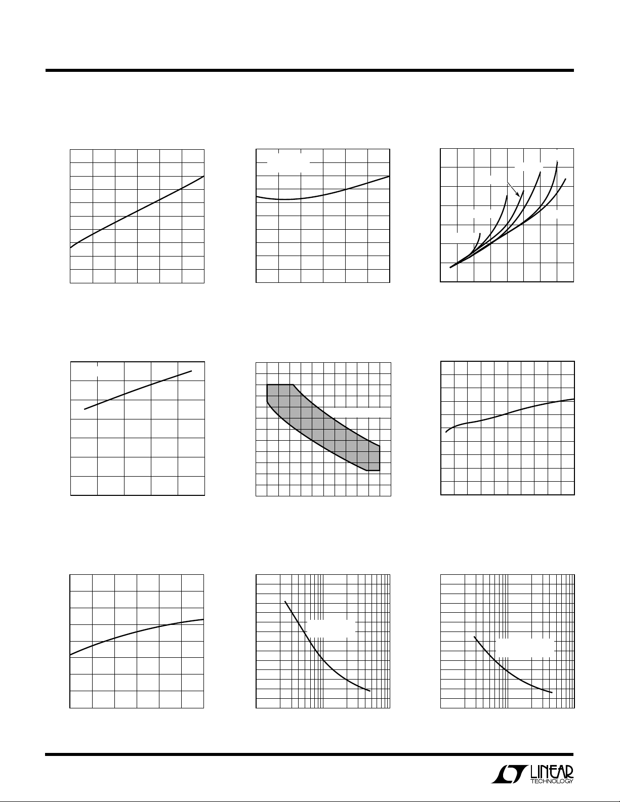
UW
Y
PICA
78
76
74
72
70
68
66
DUTY CYCLE (%)
64
62
60
58
–50 –25 0 25
1.4
1.2
1.0
0.8
0.6
ON VOLTAGE (V)
0.4
0.2
0
LPER
F
O
R
AT
CCHARA TERIST
E
C
ICS
Saturation Voltage
Duty Cycle Switch Saturation Voltage Step-Up Mode
50 75 100
TEMPERATURE (°C)
LT1110 • TPC04
500
VIN = 1.5V
450
400
350
300
(mV)
250
CESAT
200
V
150
100
50
0
= 500mA
I
SW
–50 – 25 0 25
50 75 100
TEMPERATURE (°C)
LT1110 • TPC05
Switch On Voltage Minimum/Maximum Frequency vs
Step-Down Mode On Time Quiescent Current
VIN = 12V
0 0.2 0.4 0.6
I
(A)
SWITCH
0.8 1.0
LT1110 • TPC07
100
95
90
85
80
75
70
65
60
55
OSCILLATOR FREQUENCY (KHz)
50
45
40
7
9
8
10
SWITCH ON TIME (µs)
0°C ≤ TA ≤ 70°C
11
12
LT1110 • TPC08
13
500
450
400
350
300
250
200
QUIESCENT CURRENT (µA)
150
100
–50
4
Quiescent Current R
–25
0 25 50 75 100
TEMPERATURE (°C)
LT1110 • TPC10
1.5
1.3
1.1
0.9
0.7
0.5
SWITCH CURRENT (A)
0.3
0.1
Maximum Switch Current vs Maximum Switch Current vs
Step-Up R
LIM
STEP-UP MODE
≤ 5V
V
IN
10
100
R
(Ω)
LIM
1000
LT1110 • TPC11
Step-Down
LIM
Page 5
UW
Y
PICA
160
140
120
100
80
60
BIAS CURRENT (nA)
40
20
0
–50
LPER
Set Pin Bias Current FB Pin Bias Current Reference Voltage
–25
0 25 50 75 100
TEMPERATURE (°C)
F
O
R
AT
LT1110 • TPC13
CCHARA TERIST
E
C
120
110
100
90
80
70
60
50
40
BIAS CURRENT (nA)
30
20
10
0
–25
–50
ICS
0 25 50 75 100
TEMPERATURE (°C)
LT1110 • TPC14
226
224
222
220
(mV)
REF
218
V
216
214
212
–50 –25 0 25
50 75 100
TEMPERATURE (°C)
L T1110
LT1110 • TPC15
U
PI
I
FUUC
(Pin 1): Connect this pin to VIN for normal use. Where
LIM
TI
O
U
S
lower current limit is desired, connect a resistor between
I
and VIN. A 220Ω resistor will limit the switch current
LIM
to approximately 400mA.
V
(Pin 2): Input supply voltage.
IN
SW1 (Pin 3): Collector of power transistor. For step-up
mode connect to inductor/diode. For step-down mode
connect to VIN.
SW2 (Pin 4): Emitter of power transistor. For step-up
mode connect to ground. For step-down mode connect to
inductor/diode. This pin must never be allowed to go more
than a Schottky diode drop below ground.
W
LT
1110
BLOCK
IDAGRA
V
IN
SET
+
A2
–
GAIN BLOCK/ERROR AMP
GND (Pin 5): Ground.
AO (Pin 6): Auxiliary Gain Block (GB) output. Open collector,
can sink 300µA.
SET (Pin 7): GB input. GB is an op amp with positive input
connected to SET pin and negative input connected to
220mV reference.
FB/SENSE (Pin 8): On the LT1110 (adjustable) this pin
goes to the comparator input. On the LT1110-5 and
LT1110-12, this pin goes to the internal application resistor
that sets output voltage.
AO
220mV
REFERENCE
GND
I
LIM
A1
COMPARATOR
FB
OSCILLATOR
DRIVER
SW1
Q1
SW2
LT1110 • BD01
5
Page 6

LT1110
-
VmV
R
R
OUT
=
()
+
220
2
1
101.()
1110
LT
OPER
AT
U
O
I
The LT1110 is a gated oscillator switcher. This type
architecture has very low supply current because the
switch is cycled only when the feedback pin voltage drops
below the reference voltage. Circuit operation can best be
understood by referring to the LT1110 block diagram
above. Comparator A1 compares the FB pin voltage with
the 220mV reference signal. When FB drops below
220mV, A1 switches on the 70kHz oscillator. The driver
amplifier boosts the signal level to drive the output NPN
power switch Q1. An adaptive base drive circuit senses
switch current and provides just enough base drive to
ensure switch saturation without overdriving the switch,
resulting in higher efficiency. The switch cycling action
raises the output voltage and FB pin voltage. When the FB
voltage is sufficient to trip A1, the oscillator is gated off. A
small amount of hysteresis built into A1 ensures loop
stability without external frequency compensation. When
the comparator is low the oscillator and all high current
circuitry is turned off, lowering device quiescent current to
just 300µA for the reference, A1 and A2.
The oscillator is set internally for 10µs ON time and 5µs
OFF time, optimizing the device for step-up circuits where
V
≈ 3VIN, e.g., 1.5V to 5V. Other step-up ratios as well
OUT
as step-down (buck) converters are possible at slight
losses in maximum achievable power output.
A2 is a versatile gain block that can serve as a low battery
detector, a linear post regulator, or drive an under voltage
lockout circuit. The negative input of A2 is internally
connected to the 220mV reference. An external resistor
divider from VIN to GND provides the trip point for A2. The
AO output can sink 300µA (use a 47k resistor pull up to
+5V). This line can signal a microcontroller that the battery
voltage has dropped below the preset level. To prevent the
gain block from operating in its linear region, a 2MΩ
resistor can be connected from AO to SET. This provides
positive feedback.
A resistor connected between the I
pin and VIN adjusts
LIM
maximum switch current. When the switch current exceeds the set value, the switch is turned off. This feature
is especially useful when small inductance values are used
with high input voltages. If the internal current limit of 1.5A
is desired, I
should be tied directly to VIN. Propagation
LIM
delay through the current limit circuitry is about 700ns.
In step-up mode, SW2 is connected to ground and SW1
drives the inductor. In step-down mode, SW1 is connected to VIN and SW2 drives the inductor. Output voltage
is set by the following equation in either step-up or stepdown modes where R1 is connected from FB to GND and
R2 is connected from V
OUT
to FB.
V
IN
-5, -12
SET
R1
300kΩ
+
–
R2
1110
LT
220mV
REF
GND
6
BLOCK
A2
GAIN BLOCK/ERROR AMP
A1
COMPARATOR
SENSE
IDAGRA
AO
OSCILLATOR
LT1110-5:
LT1110-12:
I
LIM
DRIVER
R1 = 13.8kΩ
R2 = 5.6kΩ
LT1110 • BD02
W
SW1
SW2
U
LT
1110
-5, -12
OPEROAT
The LT1110-5 and LT1110-12 fixed output voltage versions have the gain setting resistors on-chip. Only three
external components are required to construct a 5V or 12V
output converter. 16µA flows through R1 and R2 in the
LT1110-5, and 39µA flows in the LT1110-12. This current
represents a load and the converter must cycle from time
Q1
to time to maintain the proper output voltage. Output
ripple, inherently present in gated oscillator designs, will
typically run around 90mV for the LT1110-5 and 200mV
for the LT1110-12 with the proper inductor/capacitor
selection. This output ripple can be reduced considerably
by using the gain block amp as a pre-amplifier in front of
the FB pin. See the Applications section for details.
I
Page 7

L T1110
P
f
L
OSC
()02
It
V
R
e
L
IN
Rt
L
()
'
–()
–'
=
103
It
V
L
t
L
IN
()
= ()04
ELI
L
PEAK
=
1
2
052()
P V V V mA mW
L
=+
()()
=12 0 5 4 5 120 960 06.–. .()
P
f
mW
kHz
J
L
OSC
==
960
70
13 7 07.. ()µ
U
O
PPLICATI
A
Inductor Selection — General
A DC-DC converter operates by storing energy as magnetic flux in an inductor core, and then switching this
energy into the load. Since it is flux, not charge, that is
stored, the output voltage can be higher, lower, or opposite in polarity to the input voltage by choosing an appropriate switching topology. To operate as an efficient energy transfer element, the inductor must fulfill three requirements. First, the inductance must be low enough for
the inductor to store adequate energy under the worst
case condition of minimum input voltage and switch ON
time. The inductance must also be high enough so maximum current ratings of the LT1110 and inductor are not
exceeded at the other worst case condition of maximum
input voltage and ON time. Additionally, the inductor core
must be able to store the required flux; i.e., it must not
saturate
LT1110 based designs, small surface mount ferrite core
units with saturation current ratings in the 300mA to 1A
range and DCR less than 0.4Ω (depending on application)
are adequate. Lastly, the inductor must have sufficiently
low DC resistance so excessive power is not lost as heat
in the windings. An additional consideration is ElectroMagnetic Interference (EMI). Toroid and pot core type
inductors are recommended in applications where EMI
must be kept to a minimum; for example, where there are
sensitive analog circuitry or transducers nearby. Rod core
types are a less expensive choice where EMI is not a
problem. Minimum and maximum input voltage, output
voltage and output current must be established before an
inductor can be selected.
Inductor Selection — Step-Up Converter
In a step-up, or boost converter (Figure 4), power generated by the inductor makes up the difference between
input and output. Power required from the inductor is
determined by
. At power levels generally encountered with
S
I FOR ATIO
WU
U
Energy required by the inductor per cycle must be equal or
greater than
in order for the converter to regulate the output.
When the switch is closed, current in the inductor builds
according to
where R' is the sum of the switch equivalent resistance
(0.8Ω typical at 25°C) and the inductor DC resistance.
When the drop across the switch is small compared to VIN,
the simple lossless equation
can be used. These equations assume that at t = 0,
inductor current is zero. This situation is called “discontinuous mode operation” in switching regulator parlance.
Setting “t” to the switch ON time from the LT1110 specification table (typically 10µs) will yield I
“L” and VIN. Once I
at the end of the switch ON time can be calculated as
EL must be greater than PL/f
the required power. For best efficiency I
kept to 1A or less. Higher switch currents will cause
excessive drop across the switch resulting in reduced
efficiency. In general, switch current should be held to as
low a value as possible in order to keep switch, diode and
inductor losses at a minimum.
As an example, suppose 12V at 120mA is to be generated
from a 4.5V to 8V input. Recalling equation (01),
is known, energy in the inductor
PEAK
for the converter to deliver
OSC
for a specific
PEAK
should be
PEAK
PV VV I
=+
()()
L OUT D IN
where VD is the diode drop (0.5V for a 1N5818 Schottky).
–()01
MIN
OUT
Energy required from the inductor is
7
Page 8

LT1110
L
VVV
I
t
IN MIN SW OUT
PEAK
ON
=•
––
()11
I
mA
mA
PEAK
=
()
+
+
=
2 250
069
505
91505
498 12
.
.
–. .
.( )
L
mA
sH=•=
9155
498
10 50 13
–.–
.()µµ
PV VI
L OUT D OUT
=+
()()
|| . ()14
U
O
PPLICATI
A
Picking an inductor value of 47µH with 0.2Ω DCR results
in a peak switch current of
V
45
I
PEAK
Substituting I
EHAJ
L
Since 17.5µJ > 13.7µJ, the 47µH inductor will work. This
trial-and-error approach can be used to select the optimum inductor. Keep in mind the switch current maximum
rating of 1.5A. If the calculated peak current exceeds this,
an external power transistor can be used.
A resistor can be added in series with the I
switch current limit. The resistor should be picked such
that the calculated I
Maximum Switch Current (from Typical Performance
Characteristic curves). Then, as VIN increases, switch
current is held constant, resulting in increasing efficiency.
.
=−
W
10
.
PEAK
1
=
47 0 862 17 5 09
µµ...()
()( )
2
S
I FOR ATIO
−•
10 10
1 862 08
.
emA
47
into Equation 05 results in
at minimum VIN is equal to the
PEAK
s
Wm
H
m
2
=
WU
=
.()
pin to invoke
LIM
U
V
= output voltage
OUT
VIN = minimum input voltage
VSW is actually a function of switch current which is in turn
a function of VIN, L, time and V
be used for VSW as a very conservative value.
Once I
where tON = switch ON time (10µs).
Next, the current limit resistor R
I
PEAK
of this resistor keeps maximum switch current constant as
the input voltage is increased.
As an example, suppose 5V at 250mA is to be generated
from a 9V to 18V input. Recalling Equation (10),
is known, inductor value can be derived from
PEAK
from the R
Step-Down Mode curve. The addition
LIM
. To simplify, 1.5V can
OUT
is selected to give
LIM
Inductor Selection — Step-Down Converter
The step-down case (Figure 5) differs from the step-up in
that the inductor current flows through the load during
both the charge and discharge periods of the inductor.
Current through the switch should be limited to ~800mA
in this mode. Higher current can be obtained by using an
external switch (see Figure 6). The I
successful operation over varying inputs.
After establishing output voltage, output current and input
voltage range, peak switch current can be calculated by the
formula
I
2
I
PEAK
where DC = duty cycle (0.69)
VSW = switch drop in step-down mode
VD = diode drop (0.5V for a 1N5818)
I
OUT OUT D
=
DC
= output current
OUT
VV
+
VV V
IN SW D
pin is the key to
LIM
+
10–()
Next, inductor value is calculated using Equation (11)
Use the next lowest standard value (47µH).
Then pick R
R
= 82Ω.
LIM
Inductor Selection — Positive-to-Negative Converter
Figure 7 shows hookup for positive-to-negative conversion. All of the output power must come from the inductor.
In this case,
In this mode the switch is arranged in common collector
or step-down mode. The switch drop can be modeled as
a 0.75V source in series with a 0.65Ω resistor. When the
from the curve. For I
LIM
= 500mA,
PEAK
8
Page 9

L T1110
PPLICATI
A
U
O
S
I FOR ATIO
WU
U
switch closes, current in the inductor builds according to
V
L
I
+
()
L
=
–()
115
'
R
where R' = 0.65Ω + DCR
e
L
L
Rt
–'
VL = VIN – 0.75V
As an example, suppose –5V at 75mA is to be generated
from a 4.5V to 5.5V input. Recalling Equation (14),
PVVmAmW
=− +
()()
L
=||..()5 0 5 75 413 16
Energy required from the inductor is
P
f
OSC
413
L
mW
==
70
kHz
59 17.. ()µ
J
Picking an inductor value of 56µH with 0.2Ω DCR results
in a peak switch current of
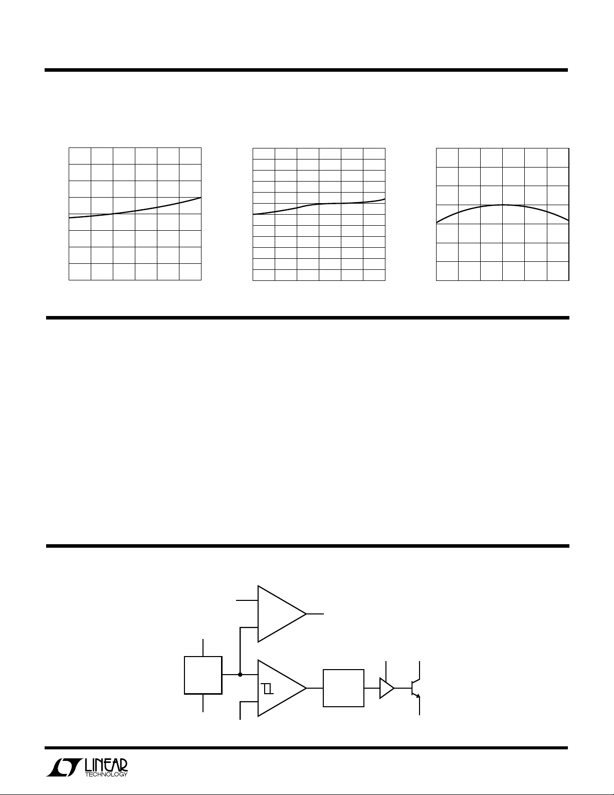
capacitors provide still better performance at more expense. We recommend OS-CON capacitors from Sanyo
Corporation (San Diego, CA). These units are physically
quite small and have extremely low ESR. To illustrate,
Figures 1, 2 and 3 show the output voltage of an LT1110
based converter with three 100µF capacitors. The peak
switch current is 500mA in all cases. Figure 1 shows a
Sprague 501D, 25V aluminum capacitor. V
jumps by
OUT
over 120mV when the switch turns off, followed by a drop
in voltage as the inductor dumps into the capacitor. This
works out to be an ESR of over 240mΩ. Figure 2 shows the
same circuit, but with a Sprague 150D, 20V tantalum
capacitor replacing the aluminum unit. Output jump is
now about 35mV, corresponding to an ESR of 70mΩ.
Figure 3 shows the circuit with a 16V OS-CON unit. ESR is
now only 20mΩ.
s
•
085 10
–.
45 075
.–.
VV
I
PEAK
Substituting I
EHAJ
()
=
065 02
..
+
ΩΩ
()
PEAK
1
=
56 0 621 10 8 19
µµ...()
()( )
L
2
1 621 18
–.()
into Equation (04) results in
Ωµ
emA
56
2
=
H
µ
=
Since 10.8µJ > 5.9µJ, the 56µH inductor will work.
With this relatively small input range, R
necessary and the I
pin can be tied directly to VIN. As in
LIM
is not usually
LIM
the step-down case, peak switch current should be limited
to ~800mA.
Capacitor Selection
Selecting the right output capacitor is almost as important
as selecting the right inductor. A poor choice for a filter
capacitor can result in poor efficiency and/or high output
ripple. Ordinary aluminum electrolytics, while inexpensive
and readily available, may have unacceptably poor Equivalent Series Resistance (ESR) and ESL (inductance). There
are low ESR aluminum capacitors on the market specifically designed for switch mode DC-DC converters which
work much better than general-purpose units. Tantalum
50mV/DIV
50mV/DIV
50mV/DIV
5 s/DIV
µ
Figure 1. Aluminum
5 s/DIV
µ
Figure 2. Tantalum
5 s/DIV
µ
Figure 3. OS-CON
LT1110 • TA19
LT1110 • TA20
LT1110 • TA21
9
Page 10

LT1110
V
R
R
mV
OUT
=+
()
1
2
1
220 21.()
LT1110 • TA15
GND
SW2
SW1
LIM
I
IN
V
R3
220
FB
V
OUT
+
C2
+
C1
D1
1N5818
V
IN
R2
R1
L1
Ω
LT1110
I
V
VV
L
t
PEAK
IN
SW OUT
ON
=
−−
.()22
PPLICATI
A
U
O
S
I FOR ATIO
WU
U
Diode Selection
Speed, forward drop, and leakage current are the three
main considerations in selecting a catch diode for LT1110
converters. General purpose rectifiers such as the 1N4001
are
unsuitable
for use in
any
switching regulator applica-
tion. Although they are rated at 1A, the switching time of
a 1N4001 is in the 10µs-50µs range. At best, efficiency will
be severely compromised when these diodes are used; at
worst, the circuit may not work at all. Most LT1110 circuits
will be well served by a 1N5818 Schottky diode, or its
surface mount equivalent, the MBRS130T3. The combination of 500mV forward drop at 1A current, fast turn ON and
turn OFF time, and 4µA to 10µA leakage current fit nicely
with LT1110 requirements. At peak switch currents of
100mA or less, a 1N4148 signal diode may be used. This
diode has leakage current in the 1nA-5nA range at 25°C
and lower cost than a 1N5818. (You can also use them to
get your circuit up and running, but beware of destroying
the diode at 1A switch currents.)
Immediately after switch turn off, the SW1 voltage pin
starts to rise because current cannot instantaneously stop
flowing in L1. When the voltage reaches V
+ VD, the
OUT
inductor current flows through D1 into C1, increasing
V
. This action is repeated as needed by the LT1110 to
OUT
keep VFB at the internal reference voltage of 220mV. R1
and R2 set the output voltage according to the formula
Step-Down (Buck Mode) Operation
A step-down DC-DC converter converts a higher voltage
to a lower voltage. The usual hookup for an LT1110 based
step-down converter is shown in Figure 5.
Step-Up (Boost Mode) Operation
A step-up DC-DC converter delivers an output voltage
higher than the input voltage. Step-up converters are
short circuit protected since there is a DC path from input
to output.
The usual step-up configuration for the LT1110 is shown
in Figure 4. The LT1110 first pulls SW1 low causing VIN –
V
to appear across L1. A current then builds up in L1.
CESAT
At the end of the switch ON time the current in L1 is1:
V
IN
t
= ()20
ON
L
L1
R3*
V
I
LIM
GND SW2
Figure 4. Step-Up Mode Hookup.
LT1110
IN
SW1
FB
D1
R2
+
C1
R1
LT1110 • TA14
10
I
PEA K
V
IN
* = OPTIONAL
V
not
OUT
Figure 5. Step-Down Mode Hookup
When the switch turns on, SW2 pulls up to V
puts a voltage across L1 equal to VIN – VSW – V
– VSW. This
IN
OUT
,
causing a current to build up in L1. At the end of the switch
ON time, the current in L1 is equal to
When the switch turns off, the SW2 pin falls rapidly and
actually goes below ground. D1 turns on when SW2
reaches 0.4V below ground. D1
DIODE
. The voltage at SW2 must never be allowed to go
MUST BE A SCHOTTKY
below – 0.5V. A silicon diode such as the 1N4933 will allow
SW2 to go to –0.8V, causing potentially destructive power
Note 1: This simple expression neglects the effects of switch and coil
resistance. This is taken into account in the “Inductor Selection” section.
Page 11

L T1110
VVV V
SW R SAT
=+ ≈
1
09 24.. ()
PPLICATI
A
U
O
S
I FOR ATIO
WU
U
dissipation inside the LT1110. Output voltage is determined by
V
OUT
=+
1
R
2
R
1
mV
220 23.()
()
R3 programs switch current limit. This is especially important in applications where the input varies over a wide
range. Without R3, the switch stays on for a fixed time
each cycle. Under certain conditions the current in L1 can
build up to excessive levels, exceeding the switch rating
and/or saturating the inductor. The 220Ω resistor programs the switch to turn off when the current reaches
approximately 800mA. When using the LT1110 in stepdown mode, output voltage should be limited to 6.2V or
less. Higher output voltages can be accommodated by
inserting a 1N5818 diode in series with the SW2 pin
(anode connected to SW2).
Higher Current Step-Down Operation
Output current can be increased by using a discrete PNP
pass transistor as shown in Figure 6. R1 serves as a
current limit sense. When the voltage drop across R1
equals a VBE, the switch turns off. For temperature compensation a Schottky diode can be inserted in series with
the I
pin. This also lowers the maximum drop across R1
LIM
to VBE – VD, increasing efficiency. As shown, switch
current is limited to 2A. Inductor value can be calculated
based on formulas in the “Inductor Selection Step-Down
R1
V
GND
0.3Ω
IN
LT1110
I
SW2
L
SW1
FB
V
25V
MAX
IN
+
C2
Figure 6. Q1 Permits Higher-Current Switching.
LT1110 Functions as Controller.
MJE210 OR
ZETEX ZTX789A
R2
220
R3
330
Q1
L1
D1
1N5821
R4
R5
V
= 220mV (1 + )
OUT
V
OUT
+
C1
R4
R5
LT1110 • TA16
Converter” section with the following conservative expression for VSW:
R2 provides a current path to turn off Q1. R3 provides base
drive to Q1. R4 and R5 set output voltage.
Inverting Configurations
The LT1110 can be configured as a positive-to-negative
converter (Figure 7), or a negative-to-positive converter
(Figure 8). In Figure 7, the arrangement is very similar to
a step-down, except that the high side of the feedback is
referred to ground. This level shifts the output negative. As
in the step-down mode, D1 must be a Schottky diode,
and V
should be less than 6.2V. More negative out-
OUT
put voltages can be accommodated as in the prior section.
+V
IN
R3
V
I
LIM
+
C2
IN
LT1110
GND
SW1
SW2
FB
L1
D1
1N5818
+
R1
C1
R2
–V
OUT
LT1110 • TA03
Figure 7. Positive-to-Negative Converter
In Figure 8, the input is negative while the output is
positive. In this configuration, the magnitude of the input
voltage can be higher or lower than the output voltage. A
level shift, provided by the PNP transistor, supplies proper
polarity feedback information to the regulator.
L1
V
I
+
C2
AO
GND SW2
–V
IN
LIM
IN
SW1
LT1110
FB
Figure 8. Negative-to-Positive Converter
D1
+V
+
C1
R2
R1
V
= 220mV + 0.6V
( )
OUT
R2
OUT
R1
2N3906
LT1110 • TA04
11
Page 12

LT1110
PPLICATI
A
Using the I
LIM
Pin
U
O
S
I FOR ATIO
WU
U
The LT1110 switch can be programmed to turn off at a set
switch current, a feature not found on competing devices.
This enables the input to vary over a wide range without
exceeding the maximum switch rating or saturating the
inductor. Consider the case where analysis shows the
LT1110 must operate at an 800mA peak switch current
with a 2.0V input. If VIN rises to 4V, peak current will rise
to 1.6A, exceeding the maximum switch current rating.
With the proper resistor selected (see the “Maximum
Switch Current vs R
” characteristic), the switch current
LIM
will be limited to 800mA, even if the input voltage
increases.
Another situation where the I
feature is useful occurs
LIM
when the device goes into continuous mode operation.
This occurs in step-up mode when
V
+
OUT DIODE
V
<
VV DC
−
IN SW
−11
25.()
switch ON times less than 3µs. Resistor values programming switch ON time for 800ns or less will cause spurious
response in the switch circuitry although the device will
still maintain output regulation.
I
L
ON
SWITCH
OFF
Figure 9. No Current Limit Causes Large Inductor
Current Build-Up
PROGRAMMED CURRENT LIMIT
I
L
LT1110 • TA05
When the input and output voltages satisfy this relationship, inductor current does not go to zero during the
switch OFF time. When the switch turns on again, the
current ramp starts from the non-zero current level in the
inductor just prior to switch turn on. As shown in Figure 9,
the inductor current increases to a high level before the
comparator turns off the oscillator. This high current can
cause excessive output ripple and requires oversizing the
output capacitor and inductor. With the I
feature,
LIM
however, the switch current turns off at a programmed
level as shown in Figure 10, keeping output ripple to a
minimum.
Figure 11 details current limit circuitry. Sense transistor
Q1, whose base and emitter are paralleled with power
switch Q2, is ratioed such that approximately 0.5% of Q2’s
collector current flows in Q1’s collector. This current is
passed through internal 80Ω resistor R1 and out through
the I
between I
switch current flows to develop a VBE across R1 + R
pin. The value of the external resistor connected
LIM
and VIN set the current limit. When sufficient
LIM
LIM
, Q3
turns on and injects current into the oscillator, turning off
the switch. Delay through this circuitry is approximately
800ns. The current trip point becomes less accurate for
ON
SWITCH
OFF
LT1110 • TA06
Figure 10. Current Limit Keeps Inductor Current Under Control
R
V
IN
Q3
OSCILLATOR
Figure 11. LT1110 Current Limit Circuitry
(EXTERNAL)
DRIVER
LIM
I
LIM
R1
80Ω
(INTERNAL)
Q1
SW1
Q2
SW2
LT1110 • TA17
Using the Gain Block
The gain block (GB) on the LT1110 can be used as an error
amplifier, low battery detector or linear post regulator. The
gain block itself is a very simple PNP input op amp with an
open collector NPN output. The negative input of the gain
block is tied internally to the 220mV reference. The positive input comes out on the SET pin.
12
Page 13

L T1110
L1
LT1110 • TA08
GND SW2
SET
SW1
LIM
I
IN
V
D1
R3
270k
FB
+
V
OUT
R2
R1
C1
V = + 1 220mV
OUT
R2
R1
( ) ( )
LT1110
AO
V
BAT
PPLICATI
A
U
O
S
I FOR ATIO
WU
U
Arrangement of the gain block as a low battery detector is
straightforward. Figure 12 shows hookup. R1 and R2 need
only be low enough in value so that the bias current of the
SET input does not cause large errors. 33kΩ for R2 is
adequate. R3 can be added to introduce a small amount of
hysteresis. This will cause the gain block to “snap” when
the trip point is reached. Values in the 1M-10M range are
optimal. The addition of R3 will change the trip point,
however.
+5V
V
IN
R1
220mV
V
BAT
R2
REF
SET
–
+
LT1110
AO
GND
R3
47k
TO
PROCESSOR
Output ripple of the LT1110, normally 90mV at 5V
OUT
can
be reduced significantly by placing the gain block in front
of the FB input as shown in Figure 13. This effectively
reduces the comparator hysteresis by the gain of the gain
block. Output ripple can be reduced to just a few millivolts
using this technique. Ripple reduction works with stepdown or inverting modes as well. For this technique to be
effective, output capacitor C1 must be large, so that each
switching cycle increases V
by only a few millivolts.
OUT
1000µF is a good starting value.
– 220mV
V
LB
R1 =
( )
4.33µA
= BATTERY TRIP POINT
V
LB
R2 = 33kΩ
R3 = 2MΩ
Figure 12. Setting Low Battery Detector Trip Point
Table 1. Inductor Manufacturers
MANUFACTURER PART NUMBERS
Coiltronics International CTX100-4 Series
984 S.W. 13th Court Surface Mount
Pompano Beach, FL 33069
305-781-8900
Sumida Electric Co. USA CD54
708-956-0666 CDR74
CDR105
Surface Mount
LT1110 • TA07
Figure 13. Output Ripple Reduction Using Gain Block
Table 2. Capacitor Manufacturers
MANUFACTURER PART NUMBERS
Sanyo Video Components OS-CON Series
2001 Sanyo Avenue
San Diego, CA 92173
619-661-6835
Nichicon America Corporation PL Series
927 East State Parkway
Schaumberg, IL 60173
708-843-7500
Sprague Electric Company 150D Solid Tantalums
Lower Main Street 550D Tantalex
Sanford, ME 04073
207-324-4140
Matsuo 267 Series
714-969-2491 Surface Mount
Table 3. Transistor Manufacturers
MANUFACTURER PART NUMBERS
Zetex ZTX Series
Commack, NY FZT Series
516-543-7100 Surface Mount
13
Page 14

LT1110
U
O
PPLICATITYPICAL
SA
All Surface Mount
Flash Memory VPP Generator
+5V
±10%
= PROGRAM
1
= SHUTDOWN
0
L1*
47µH
MMBT4403
10k
V
I
LIM
+
22µF
1k
MMBF170
LT1110CS8-12
GND SW2
*L1= SUMIDA CD105-470M
IN
SW1
SENSE
MBRS12OT3
+
47µF
20V
LT1110 • TA18
V
PP
12V
120MA
1.5V Powered Laser Diode Driver
TOSHIBA
TOLD-9211
22nF
4.7k
2N3906
1N4148
1.5V
ADJUST R1 FOR CHANGE IN LASER OUTPUT POWER
*
✝
TOKO 262LYF-0076M
LASER DIODE CASE COMMON TO +BATTERY TERMINAL
•
170mA CURRENT DRAIN FROM 1.5V CELL (50mA DIODE)
•
NO OVERSHOOT
•
12
I
LIM
6
AO
LT1110
8
FB
GND SW2
V
IN
3
SW1
7
SET
45
1.5V Powered Laser Diode Driver
220Ω
10
Ω
1k*
R1
MJE210
1N5818
✝
L1
2.2 H
0.22 F
µ
C1
+
100 F
OS-CON
µ
CERAMIC
µ
2Ω
LT1110 • TA13
14
Page 15

L T1110
LT1110 • TA12
GND SW2
SENSE
SW1
LIM
I
IN
V
LT1110
1.5V
AA OR
AAA
CELL
= MBRL120
= COILCRAFT 1812LS-823
4.7µF
L1*
82µH
+5V
4mA
4.7µF
–5V
4mA
4.7µF
+
+
*L1
+
U
O
PPLICATITYPICAL
SA
All Surface Mount
3V to 5V Step-Up Converter
L1*
47µH
220
V
I
LIM
3V
2x
AA CELL
GND SW2
*L1 = COILCRAFT 1812LS-473
LT1110-5
IN
SW1
SENSE
+
MBRL120
5V
40mA
10µF
LT1110 • TA09
All Surface Mount
1.5V to +10V, +5V Dual Output Step-Up Converter
All Surface Mount
9V to 5V Step-Down Converter
220
V
I
LIM
9V
GND SW2
*L1 = COILCRAFT 1812LS-473
LT1110-5
IN
SW1
SENSE
47µH
MBRL120
L1*
+
10µF
LT1110 • TA10
All Surface Mount
1.5V to ±5V Dual Output Step-Up Converter
5V
40mA
*L1
I
LIM
GND SW2
LT1110
1.5V
AA OR
AAA
CELL
= MBRL120
= COILCRAFT 1812LS-823
L1*
82µH
V
IN
SW1
FB
4.7µF
+
490k
+
Information furnished by Linear Technology Corporation is believed to be accurate and reliable.
However, no responsibility is assumed for its use. Linear Technology Corporation makes no representation that the interconnection of its circuits as described herein will not infringe on existing patent rights.
4.7µF
11k
+
LT1110 • TA11
+10V
3mA
+5V
3mA
4.7µF
15
Page 16

LT1110
PACKAGEDESCRIPTI
0.300 – 0.320
(7.620 – 8.128)
U
Dimensions in inches (millimeters) unless otherwise noted.
O
N8 Package
8-Lead Plastic DIP
0.045 – 0.065
(1.143 – 1.651)
0.130 ± 0.005
(3.302 ± 0.127)
0.400
(10.160)
MAX
876
5
0.065
(1.651)
0.009 – 0.015
(0.229 – 0.381)
+0.025
0.325
–0.015
+0.635
8.255
()
–0.381
0.010 – 0.020
(0.254 – 0.508)
0.008 – 0.010
(0.203 – 0.254)
*THESE DIMENSIONS DO NOT INCLUDE MOLD FLASH OR PROTRUSIONS.
MOLD FLASH OR PROTRUSIONS SHALL NOT EXCEED 0.006 INCH (0.15mm).
× 45°
0.016 – 0.050
0.406 – 1.270
TYP
0.045 ± 0.015
(1.143 ± 0.381)
0.100 ± 0.010
(2.540 ± 0.254)
0°– 8° TYP
0.053 – 0.069
(1.346 – 1.752)
0.014 – 0.019
(0.355 – 0.483)
0.125
(3.175)
MIN
0.018 ± 0.003
(0.457 ± 0.076)
S8 Package
8-Lead Plastic SOIC
0.004 – 0.010
(0.101 – 0.254)
0.050
(1.270)
BSC
0.020
(0.508)
MIN
12
0.228 – 0.244
(5.791 – 6.197)
3
0.189 – 0.197*
(4.801 – 5.004)
7
8
1
2
4
6
3
0.250 ± 0.010
(6.350 ± 0.254)
5
0.150 – 0.157*
(3.810 – 3.988)
4
16
Linear Technology Corporation
1630 McCarthy Blvd., Milpitas, CA 95035-7487
(408) 432-1900
●
FAX
: (408) 434-0507
●
TELEX
: 499-3977
LT/GP 0594 2K REV B • PRINTED IN USA
LINEAR TECHNOLOGY CORPORATION 1994
 Loading...