

Page 1
LT1108
Micropower
DC/DC Converter
Adjustable and Fixed 5V, 12V
EATU
F
■
Operates at Supply Voltages from 2V to 30V
■
Consumes Only 110µA Supply Current
■
Works in Step-Up or Step-Down Mode
■
Only Four External Components Required
■
Low Battery Detector Comparator On-Chip
■
User Adjustable Current Limit
■
Internal 1A Power Switch
■
Fixed or Adjustable Output Voltage Versions
■
Space Saving 8-Pin MiniDIP or S8 Package
PPLICATI
A
■
Palmtop Computers
■
3V to 5V, 5V to 12V Converters
■
9V to 5V, 12V to 5V Converters
■
LCD Bias Generators
■
Peripherals and Add-On Cards
■
Battery Backup Supplies
■
Cellular Telephones
■
Portable Instruments
RE
S
O
U
S
DUESCRIPTIO
The LT1108 is a versatile micropower DC/DC converter.
The device requires only four external components to
deliver a fixed output of 5V or 12V. Supply voltage ranges
from 2V to 12V in step-up mode and to 30V in step-down
mode. The LT1108 functions equally well in step-up, stepdown, or inverting applications.
The LT1108 is pin-for-pin compatible with the LT1173, but
has a duty cycle of 70%, resulting in increased output
current in many applications. The LT1108 can deliver
150mA at 5V from a 2 AA cell input and 5V at 300mA from
9V in step-down mode. Quiescent current is just 110µA,
making the LT1108 ideal for power conscious batteryoperated systems.
Switch current limit can be programmed with a single
resistor. An auxiliary gain block can be configured as a low
battery detector, linear post regulator, undervoltage lockout circuit, or error amplifier.
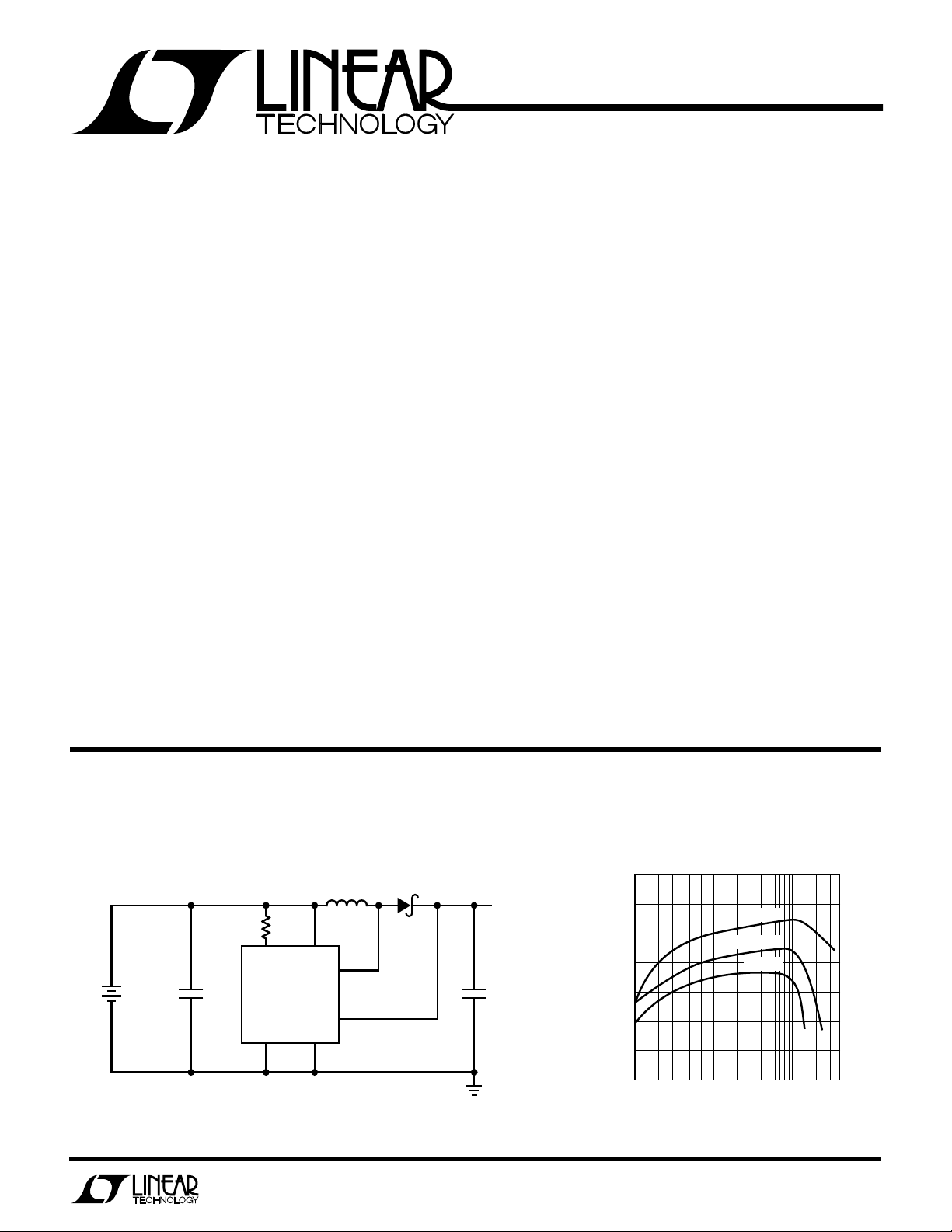
A
2 × AA
CELLS
*L1 =
+
GOWANDA GA20-103K
COILTRONICS CTX100-4
SUMIDA CD105-101K
U
O
PPLICATITYPICAL
EfficiencyPalmtop Computer Logic Supply
84
82
80
78
76
EFFICIENCY (%)
74
72
70
1
VIN = 3V
VIN = 2.5V
V
= 2V
IN
10 100
LOAD CURRENT (mA)
LT1108 • TA02
100µF
47Ω
I
LIM
GND SW2
V
LT1108-5
SENSE
IN
SW1
L1*
100µH
1N5817
+
5V
150mA
AVX
TPS
330µF
6.3V
LT1108 • TA01
1
Page 2
LT1108
A
W
O
LUTEXI T
S
A
WUW
ARB
U
G
I
S
Supply Voltage (VIN)............................................... 36V
SW1 Pin Voltage (V
SW2 Pin Voltage (V
) ......................................... 50V
SW1
) ............................ –0.5V to V
SW2
Feedback Pin Voltage (LT1108) ............................. 5.5V
Sense Pin Voltage (LT1108, -5, -12) ...................... 36V
WU
/
PACKAGE
I
LIM
V
IN
SW1
SW2
T
JMAX
O
RDER I FOR ATIO
TOP VIEW
1
2
3
4
N8 PACKAGE
8-LEAD PLASTIC DIP
*FIXED VERSIONS
= 90°C, θJA = 130°C/W
FB (SENSE*)
8
SET
7
A0
6
GND
5
ORDER PART
NUMBER
LT1108CN8
LT1108CN8-5
LT1108CN8-12
Maximum Power Dissipation ............................ 500mW
Maximum Switch Current ...................................... 1.5A
Operating Temperature Range .................... 0°C to 70°C
IN
Storage Temperature Range ................ –65°C to 150°C
Lead Temperature (Soldering, 10 sec)................. 300°C
U
ORDER PART
I
1
LIM
V
2
IN
SW1
3
SW2
4
S8 PACKAGE
8-LEAD PLASTIC SOIC
*FIXED VERSIONS
T
= 90°C, θJA = 150°C/W
JMAX
TOP VIEW
FB (SENSE*)
8
SET
7
A0
6
GND
5
NUMBER
LT1108CS8
LT1108CS8-5
LT1108CS8-12
S8 PART MARKING
1108
10805
10812
LECTRICAL C CHARA TERIST
E
SYMBOL PARAMETER CONDITIONS MIN TYP MAX UNITS
I
V
V
f
t
V
V
Q
IN
OUT
OSC
ON
OL
SAT
Quiescent Current Switch OFF ● 110 150 µA
Quiescent Current, Boost Mode Configuration No Load LT1108-5 135 µA
Input Voltage Step-Up Mode ● 2 12.6 V
Comparator Trip Point Voltage LT1108 (Note 1) ● 1.2 1.245 1.3 V
Output Sense Voltage LT1108-5 (Note 2) ● 4.75 5 5.25 V
Comparator Hysteresis LT1108 ● 510 mV
Output Hysteresis LT1108-5 ● 20 40 mV
Oscillator Frequency ● 14 19 25 kHz
Duty Cycle Full Load, Step-Up Mode ● 63 70 78 %
Switch-ON Time I
Feedback Pin Bias Current LT1108, VFB = 0V ● 10 50 nA
Set Pin Bias Current V
Gain Block Output Low I
Reference Line Regulation 2V ≤ VIN ≤ 5V ● 0.20 0.400 %/V
SW
Voltage, Step-Up Mode VIN = 3V, ISW = 650mA ● 0.5 0.65 V
SAT
ICS
TA = 25°C, VIN = 3V, unless otherwise noted.
LT1108-12 250 µA
Step-Down Mode ● 30.0 V
LT1108-12 (Note 2) ● 11.4 12 12.6 V
LT1108-12
Tied to VIN, Step-Up Mode ● 28 36 48 µs
LIM
= V
SET
REF
= 100µA, V
SINK
5V ≤ V
≤ 30V ● 0.02 0.075 %/V
IN
VIN = 5V, ISW = 1A 0.8 1.00 V
= 1V ● 0.15 0.4 V
SET
● 50 100 mV
● 20 100 nA
2
Page 3
LT1108
R
LIM
(Ω)
10
SWITCH CURRENT (mA)
100 1000
LT1108 • TPC03
1000
1200
1100
900
800
700
600
500
400
300
200
100
2V ≤ VIN ≤ 5V
LECTRICAL C CHARA TERIST
E
ICS
TA = 25°C, VIN = 3V, unless otherwise noted.
SYMBOL PARAMETER CONDITIONS MIN TYP MAX UNITS
V
SAT
A
V
SW
Voltage, Step-Down Mode VIN = 12V, ISW = 650mA 1.1 1.5 V
SAT
● 1.7 V
Gain Block Gain RL = 100k (Note 3) ● 400 1000 V/V
Current Limit 220Ω from I
LIM
to V
IN
400 mA
Current Limit Temperature Coefficient ● –0.3 %/°C
Switch OFF Leakage Current Measured at SW1 Pin 1 10 µA
V
SW2
● denotes specifications which apply over the full operating
The
temperature range.
Note 1: This specification guarantees that both the high and low trip points
of the comparator fall within the 1.2V to 1.3V range.
Maximum Excursion Below GND I
≤ 10µA, Switch OFF –400 –350 mV
SW1
Note 2: The output voltage waveform will exhibit a sawtooth shape due to
the comparator hysteresis. The output voltage on the fixed output versions
will always be within the specified range.
Note 3: 100k resistor connected between a 5V source and the A0 pin.
UW
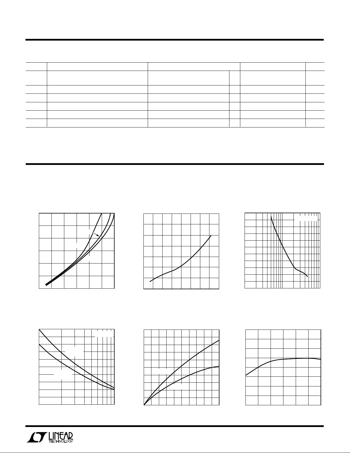
Y
PICA
1.2
LPER
F
O
R
AT
Saturation Voltage Step-Up Mode
(SW2 Pin Grounded)
CCHARA TERIST
E
C
Switch ON Voltage
Step-Down Mode
(SW1 Pin Connected to VIN)
1.4
ICS
Maximum Switch Current
vs R
LIM
1.0
0.8
(V)
0.6
CESAT
V
0.4
0.2
0
0
Saturation Voltage Step-Up Mode
(SW2 Pin Grounded)
1000
900
800
700
600
500
400
300
SWITCH CURRENT (mA)
200
100
0
100
VIN = 3V
VIN = 2V
0.4 0.6 0.8
0.2
SWITCH CURRENT (A)
VIN = 24V
L = 500µH
VIN = 12V
L = 250µH
R
(Ω)
LIM
VIN = 5V
1.0 1.2
LT1108 • TPC01
V
= 5V
OUT
LT1108 • TPC04
1000
1.3
1.2
1.1
1.0
0.9
SWITCH ON VOLTAGE (V)
0.8
0.7
0.1 0.3 0.7
0.2 0.4 0.8
0
SWITCH CURRENT (A)
0.5
0.6
LT1108 • TPC02
Supply Current vs Switch Current Quiescent Current
50
40
30
20
SUPPLY CURRENT (mA)
10
0
VIN = 5V
200
0
SWITCH CURRENT (mA)
VIN = 2V
400
600
800
LTC1108 • TPC05
1000
120
115
110
105
100
95
90
QUIESCENT CURRENT (µA)
85
80
–25 0 50
–50
25
TEMPERATURE (°C)
75
LT1108 • TPC06
3
100
Page 4
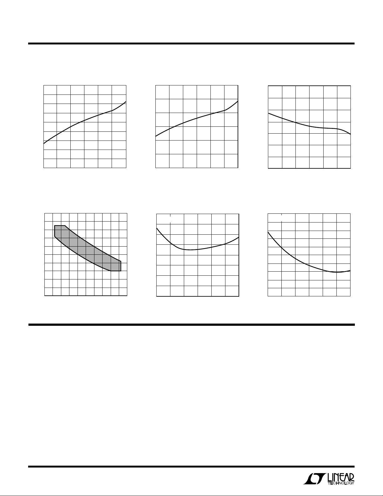
LT1108
TEMPERATURE (˚C)
–50
38
40
42
25 75
LT1108 • TPC09
36
34
–25 0
50 100
32
30
SWITCH-ON TIME (µs)
44
Y
PICA
LPER
F
O
R
AT
UW
CCHARA TERIST
E
C
ICS
Oscillator Frequency Duty Cycle Switch-ON Time
22
21
20
19
18
17
16
FREQUENCY (kHz)
15
14
13
–25 0 50
–50
25
TEMPERATURE (°C)
75
LT1108 • TPC07
100
80
75
70
65
DUTY CYCLE (%)
60
55
50
–25 0 50
–50
25
TEMPERATURE (°C)
75
LT1108 • TPC08
100
Minimum/Maximum Frequency Switch Saturation Voltage Switch Saturation Voltage
vs ON-Time Step-Up Mode Step-Down Mode
28
26
24
22
20
18
16
FREQUENCY (kHz)
14
12
10
0
30
25
40
35
ON-TIME (µs)
45
LT1108 • TPC10
0.8
ISW = 650mA
0.7
0.6
0.5
(V)
0.4
CESAT
V
0.3
0.2
0.1
50
0
–25 0 50
–50
25
TEMPERATURE (°C)
75
LT1108 • TPC11
100
(V)
SAT
V
1.8
1.6
1.5
1.4
1.2
0.8
1.7
1.3
1.1
1.0
0.9
–50
ISW = 650mA
–25
0
TEMPERATURE (°C)
25 50
75
LT1108 • TPC12
100
U
PI
I
lower current limit is desired, connect a resistor between
I
to approximately 400mA.
V
SW1 (Pin 3): Collector of power transistor. For step-up
mode connect to inductor/diode. For step-down mode
connect to VIN.
SW2 (Pin 4): Emitter of power transistor. For step-up
mode connect to ground. For step-down mode connect to
inductor/diode. This pin must never be allowed to go more
FUUC
(Pin 1): Connect this pin to VIN for normal use. Where
LIM
and VIN. A 220Ω resistor will limit the switch current
LIM
(Pin 2): Input supply voltage.
IN
TI
O
U
S
GND (Pin 5): Ground.
AO (Pin 6): Auxiliary gain block (GB) output. Open collector,
can sink 100µA.
SET (Pin 7): GB input. GB is an op amp with positive input
connected to SET pin and negative input connected to
1.245V reference.
FB/SENSE (Pin 8): On the LT1108 (adjustable) this pin
goes to the comparator input. On the LT1108-5 and
LT1108-12, this pin goes to the internal application resistor
that sets output voltage.
than a Schottky diode drop below ground.
4
Page 5

OPER
I
LIM
A2
A1
V
IN
GND
SET
A0
GAIN BLOCK/
ERROR AMP
COMPARATOR
DRIVER
SW1
SW2
1.245V
REFERENCE
OSCILLATOR
LT1108-5 • BD
SENSE
R1
R2
753k
LT1108-5: R1 = 250k
LT1108-12: R1 = 87.4k
AT
LT1108
U
O
I
The LT1108 is a gated oscillator switcher. This type
architecture has very low supply current because the
switch is cycled when the feedback pin voltage drops
below the reference voltage. Circuit operation can best be
understood by referring to the LT1108 block diagram.
Comparator A1 compares the feedback (FB) pin voltage
with the 1.245V reference signal. When FB drops below
1.245V, A1 switches on the 19kHz oscillator. The driver
amplifier boosts the signal level to drive the output NPN
power switch. The switch cycling action raises the output
voltage and FB pin voltage. When the FB voltage is sufficient to trip A1, the oscillator is gated off. A small amount
of hysteresis built into A1 ensures loop stability without
external frequency compensation. When the comparator
output is low, the oscillator and all high current circuitry
is turned off, lowering device quiescent current to just
110µA.
The oscillator is set internally for 36µs ON-time and 17µs
OFF-time, allowing continuous mode operation in many
cases such as 2V to 5V converters. Continuous mode
greatly increases available output power.
negative input of A2 is the 1.245V reference. A resistor
divider from VIN to GND, with the mid-point connected to
the SET pin provides the trip voltage in a low battery
detector application. A0 can sink 100µA (use a 47k resistor pull-up to 5V).
A resistor connected between the I
pin and VIN sets
LIM
maximum switch current. When the switch current exceeds the set value, the switch cycle is prematurely
terminated. If current limit is not used, I
should be tied
LIM
directly to VIN. Propagation delay through the currentlimit circuitry is approximately 2µs.
In step-up mode the switch emitter (SW2) is connected to
ground and the switch collector (SW1) drives the inductor; in step-down mode the collector is connected to V
IN
and the emitter drives the inductor.
The LT1108-5 and LT1108-12 are functionally identical to
the LT1108. The -5 and -12 versions have on-chip voltage
setting resistors for fixed 5V or 12V outputs. Pin 8 on the
fixed versions should be connected to the output. No
external resistors are needed.
Gain block A2 can serve as a low battery detector. The
W
BLOCK
V
1.245V
REFERENCE
GND
IDAGRA
SET
IN
FB
S
LT1108 LT1108-5/LT1108-12
A2
GAIN BLOCK/
ERROR AMP
A1
COMPARATOR
A0
OSCILLATOR
DRIVER
LT1108 • BD
I
LIM
SW1
SW2
5
Page 6

LT1108
P
f
L OSC
/()02
It
V
R
e
L
IN
Rt
L
()
'
–()
–'
=
103
It
V
L
t
L
IN
()
= ()04
ELI
L
PEAK
=
1
2
052()
P V V V mA mW
L
=+
()()
=12 0 5 2 30 315 06.– ()
U
O
PPLICATI
A
INDUCTOR SELECTION
General
A DC/DC converter operates by storing energy as magnetic flux in an inductor core, and then switching this
energy into the load. Since it is flux, not charge, that is
stored, the output voltage can be higher, lower, or opposite in polarity to the input voltage by choosing an appropriate switching topology.
To operate as an efficient energy transfer element, the
inductor must fulfill three requirements. First, the inductance must be low enough for the inductor to store adequate
energy under the worst case condition of minimum input
voltage and switch-ON time. The inductance must also be
high enough so maximum current ratings of the LT1108
and inductor are not exceeded at the other worst case
condition of maximum input voltage and ON-time.
S
I FOR ATIO
WU
U
where VD is the diode drop (0.5V for a 1N5818 Schottky).
Energy required by the inductor per cycle must be equal or
greater than
in order for the converter to regulate the output.
When the switch is closed, current in the inductor builds
according to
where R' is the sum of the switch equivalent resistance
(0.8Ω typical at 25°C) and the inductor DC resistance.
When the drop across the switch is small compared to VIN,
the simple lossless equation
Additionally, the inductor core must be able to store the
required flux; i.e., it must not
generally encountered with LT1108 based designs, small
surface mount ferrite core units with saturation current
ratings in the 300mA to 1A range and DCR less than 0.4Ω
(depending on application) are adequate.
Lastly, the inductor must have sufficiently low DC resistance so excessive power is not lost as heat in the windings.
An additional consideration is Electro-Magnetic Interference (EMI). Toroid and pot core type inductors are recommended in applications where EMI must be kept to a
minimum; for example, where there are sensitive analog
circuitry or transducers nearby. Rod core types are a less
expensive choice where EMI is not a problem. Minimum
and maximum input voltage, output voltage and output
current must be established before an inductor can be
selected.
Step-Up Converter
In a step-up, or boost converter (Figure 1), power generated
by the inductor makes up the difference between input and
output. Power required from the inductor is determined by
saturate
. At power levels
can be used. These equations assume that at t = 0,
inductor current is zero. This situation is called “discontinuous mode operation” in switching regulator parlance.
Setting “t” to the switch-ON time from the LT1108 specification table (typically 36µs) will yield I
and VIN. Once I
end of the switch-ON time can be calculated as
EL must be greater than PL/f
the required power. For best efficiency I
to 1A or less. Higher switch currents will cause excessive
drop across the switch resulting in reduced efficiency. In
general, switch current should be held to as low a value as
possible in order to keep switch, diode and inductor losses
at a minimum.
As an example, suppose 12V at 30mA is to be generated
from a 2V to 3V input. Recalling equation (01),
is known, energy in the inductor at the
PEAK
for the converter to deliver
OSC
for a specific “L”
PEAK
should be kept
PEAK
PV VV I
=+
()()
L OUT D IN
6
–()01
MIN
OUT
Page 7

LT1108
L
VVV
I
t
IN MIN SW OUT
PEAK
ON
=
−−
× ()11
I
mA
mA
PEAK
=
()
+
+
=
2 300
060
505
12 15 05
500 12
.
.
–. .
()
L
mA
sH==
12 1 5 5
500
36 396 13
–.–
()µµ
U
O
PPLICATI
A
Energy required from the inductor is
315
P
L
f
OSC
Picking an inductor value of 100µH with 0.2Ω DCR results
in a peak switch current of
I
=
PEAK
Substituting I
EHAJ
=
L
Since 18.3µJ > 16.6µJ, the 100µH inductor will work. This
trial-and-error approach can be used to select the optimum
inductor. Keep in mind the switch current maximum rating
of 1.5A. If the calculated peak current exceeds this, an
external power transistor can be used.
A resistor can be added in series with the I
switch current limit. The resistor should be picked so the
calculated I
Switch Current (from Typical Performance Characteristic
curves). Then, as VIN increases, switch current is held
constant, resulting in increasing efficiency.
mW
==
19
kHz
V
2
.
10
PEAK
1
100 6 605 18 3 09
()( )
2
PEAK
S
I FOR ATIO
16 6 07.()µ
J
×
10 36
–.ΩΩµ
emA
–()
1 605 08
into Equation 04 results in
µµ.. ()
at minimum VIN is equal to the Maximum
100
H
µ
2
=
WU
s
=
pin to invoke
LIM
U
where DC = duty cycle (0.60)
VSW = switch drop in step-down mode
VD = diode drop (0.5V for a 1N5818)
I
= output current
OUT
V
= output voltage
OUT
VIN = minimum input voltage
VSW is actually a function of switch current which is in turn
a function of VIN, L, time, and V
be used for VSW as a very conservative value.
Once I
where tON = switch-ON time (36µs).
Next, the current limit resistor R
from the R
resistor keeps maximum switch current constant as the
input voltage is increased.
As an example, suppose 5V at 300mA is to be generated
from a 12V to 24V input. Recalling Equation (10),
is known, inductor value can be derived from
PEAK
Step-Down Mode curve. The addition of this
LIM
. To simplify, 1.5V can
OUT
is selected to give I
LIM
PEAK
Step-Down Converter
The step-down case (Figure 2) differs from the step-up in
that the inductor current flows through the load during both
the charge and discharge periods of the inductor. Current
through the switch should be limited to ~650mA in this
mode. Higher current can be obtained by using an external
switch (see Figure 3). The I
operation over varying inputs.
After establishing output voltage, output current and input
voltage range, peak switch current can be calculated by the
formula:
I
PEAK
2
=
pin is the key to successful
LIM
I
OUT OUT D
DC
VV
+
VV V
IN SW D
+
10–()
Next, inductor value is calculated using Equation (11)
Use the next lowest standard value (330µH).
Then pick R
R
= 220Ω.
LIM
Positive-to-Negative Converter
Figure 4 shows hookup for positive-to-negative conversion. All of the output power must come from the inductor.
In this case,
P
= (V
L
from the curve. For I
LIM
+ V
)(I
OUT
D
) (14)
OUT
= 500mA,
PEAK
7
Page 8

LT1108
I
V
L
t
PEA K
IN
ON
= *()20
V
R
R
V
OUT
=+
()
1
2
1
1 245 21.()
L1
LT1108 • F01
GND SW2
SW1
LIM
I
IN
V
D1
R3
LT1108
+
V
OUT
R2
R1
C1
V
IN
FB
PPLICATI
A
U
O
S
I FOR ATIO
WU
U
In this mode the switch is arranged in common collector or
step-down mode. The switch drop can be modeled as a
0.75V source in series with a 0.65Ω resistor. When the
switch closes, current in the inductor builds according to
–'
V
=
L
'
R
It
()
L
where: R' = 0.65Ω + DCR
Rt
–()
e
115
L
L
VL = VIN – 0.75V
As an example, suppose –5V at 100mA is to be generated
from a 4.5V to 5.5V input. Recalling Equation (14),
P
= (–5V+ 0.5V)(100mA) = 550mW. (16)
L
Energy required from the inductor is
P
f
OSC
550
L
mW
==
19
kHz
28 9 17.()µ
J
The usual step-up configuration for the LT1108 is shown in
Figure 1. The LT1108 first pulls SW1 low causing VIN –
V
to appear across L1. A current then builds up in L1.
CESAT
At the end of the switch-ON time the current in L1 is
Figure 1. Step-Up Mode Hookup
Picking an inductor value of 220µH with 0.3Ω DCR results
in a peak switch current of
×
095 36
–.
45 075
.–.
VV
I
PEAK
Substituting I
()
=
0 ΩΩ
()
568
=
1
EHAJ
=
L
2
+
65 0 3
..
mA
into Equation (04) results in
PEAK
220 0 568 35 5 19
µµ.. ()
()()
1
–
2
Ωµ
e
220
=
µ
H
s
(18)
Since 35.5µJ > 28.9µJ, the 220µH inductor will work.
Finally, R
Current vs R
STEP-UP (BOOST MODE) OPERATION
A step-up DC/DC converter delivers an output voltage
higher than the input voltage. Step-up converters are not
short-circuit protected since there is a DC path from input
to output.
should be selected by looking at the Switch
LIM
curve. In this example, R
LIM
= 150Ω.
LIM
Immediately after switch turn-off, the SW1 voltage pin
starts to rise because current cannot instantaneously stop
flowing in L1. When the voltage reaches V
inductor current flows through D1 into C1, increasing V
This action is repeated as needed by the LT1108 to keep V
+ VD, the
OUT
OUT
.
FB
at the internal reference voltage of 1.245V. R1 and R2 set
the output voltage according to the formula
STEP-DOWN (BUCK MODE) OPERATION
A step-down DC/DC converter converts a higher voltage to
a lower voltage. The usual hookup for an LT1108 based
step-down converter is shown in Figure 2.
When the switch turns on, SW2 pulls up to V
puts a voltage across L1 equal to VIN – VSW – V
– VSW. This
IN
, causing
OUT
a current to build up in L1. At the end of the switch- ON time,
the current in L1 is equal to
*Expression 20 neglects the effect of switch and coil resistance. This is taken into account in the
"Inductor Selection" section.
8
Page 9

LT1108
VVV V
SW R Q SAT
=+ ≈
11
10 24.()
LT1108 • F03
D1
1N5821
+
+
V
OUT
V
IN
30V
MAX
L1
R1
0.15Ω
R2
100Ω
Q1
ZETEX ZTX749
R3
330Ω
R4
R5
C1
LT1108
GND
SW2
SW1
V
IN
I
L
FB
C2
R6
100Ω
V
OUT
= 1.245V 1 +
R4
R5
()
PPLICATI
A
I
=
PEAK
O
V
VV
−−
IN
SW OUT
L
U
S
I FOR ATIO
t
ON
WU
U
()22
When the switch turns off, the SW2 pin falls rapidly and
actually goes below ground. D1 turns on when SW2
reaches 0.4V below ground.
DIODE
. The voltage at SW2 must never be allowed to go
D1 MUST BE A SCHOTTKY
below –0.5V. A silicon diode such as the 1N4933 will allow
SW2 to go to –0.8V, causing potentially destructive power
dissipation inside the LT1108. Output voltage is determined by
V
OUT
=+
1
R
2
()
R
1
V
1 245 23.()
R3 programs switch current limit. This is especially important in applications where the input varies over a wide
range. Without R3, the switch stays on for a fixed time each
cycle. Under certain conditions the current in L1 can build
up to excessive levels, exceeding the switch rating and/or
saturating the inductor. The 100Ω resistor programs the
switch to turn off when the current reaches approximately
700mA. When using the LT1108 in step-down mode,
output voltage should be limited to 6.2V or less. Higher
output voltages can be accommodated by inserting a
1N5818 diode in series with the SW2 pin (anode connected
to SW2).
HIGHER CURRENT STEP-DOWN OPERATION
Output current can be increased by using a discrete PNP
pass transistor as shown in Figure 3. R1 serves as a
current limit sense. When the voltage drop across R1
equals 0.5VBE, the switch turns off. As shown, switch
current is limited to 2A. Inductor value can be calculated
based on formulas in the Inductor Selection Step-Down
Converter section with the following conservative expression for VSW:
R2 provides a current path to turn off Q1. R3 provides base
drive to Q1. R4 and R5 set output voltage. A PMOS FET can
be used in place of Q1 when VIN is between 10V and 20V.
V
IN
R3
100Ω
+
I
V
LIM
C2
Figure 2. Step-Down Mode Hookup
SW1
IN
FB
LT1108
SW2
GND
Figure 3. Q1 Permits Higher Current Switching
The LT1108 Functions as Controller
INVERTING CONFIGURATIONS
L1
D1
1N5818
V
OUT
+
C1
R2
R1
LT1108 • F02
The LT1108 can be configured as a positive-to-negative
converter (Figure 4), or a negative-to-positive converter
(Figure 5). In Figure 4, the arrangement is very similar to a
step-down, except that the high side of the feedback is
referred to ground. This level shifts the output negative. As
in the step-down mode, D1 must be a Schottky diode,
and V
should be less than 6.2V. More negative output
OUT
voltages can be accommodated as in the prior section.
In Figure 5, the input is negative while the output is positive.
In this configuration, the magnitude of the input voltage can
be higher or lower than the output voltage. A level shift,
9
Page 10

LT1108
V
V
VV DC
OUT DIODE
IN SW
+
−
<
−11
25.()
LT1108 • F06
OFF
ON
SWITCH
I
L
LT1108 • F07
ON
OFF
SWITCH
PROGRAMMED CURRENT LIMIT
I
L
PPLICATI
A
U
O
S
I FOR ATIO
WU
U
provided by the PNP transistor, supplies proper polarity
feedback information to the regulator.
V
IN
R3
–V
I
LIMVIN
+
C2
Figure 4. Positive-to-Negative Converter
I
LIM
+
C2
AO
GND SW2
IN
LT1108
GND
LT1108
V
SW1
SW2
IN
SW1
FB
L1
+
D1
1N5818
L1
C1
D1
+
FB
R2
V
= 1.245V + 0.6V
OUT
R1
R2
–V
OUT
LT1108 • F04
V
OUT
R1
C1
2N3906
R1
()
R2
LT1108 • F05
Another situation where the I
feature is useful occurs
LIM
when the device goes into continuous mode operation. This
occurs in step-up mode when
When the input and output voltages satisfy this relationship, inductor current does not go to zero during the switchOFF time. When the switch turns on again, the current ramp
starts from the non-zero current level in the inductor just
prior to switch turn-on. As shown in Figure 6, the inductor
current increases to a high level before the comparator
turns off the oscillator. This high current can cause excessive output ripple and requires oversizing the output capacitor and inductor. With the I
feature, however, the
LIM
switch current turns off at a programmed level as shown in
Figure 7, keeping output ripple to a minimum.
Figure 5. Negative-to-Positive Converter
USING THE I
LIM
The LT1108 switch can be programmed to turn off at a set
switch current, a feature not found on competing devices.
This enables the input to vary over a wide range without
exceeding the maximum switch rating or saturating the
inductor. Consider the case where analysis shows the
LT1108 must operate at an 800mA peak switch current with
a 2.0V input. If VIN rises to 4V, the peak switch current will
rise to 1.6A, exceeding the maximum switch current rating.
With the proper resistor selected (see the “Maximum
Switch Current vs R
will be limited to 800mA, even if the input voltage increases.
10
PIN
” characteristic), the switch current
LIM
Figure 6. No Current Limit Causes Large Inductor
Current Build-Up
Figure 7. Current Limit Keeps Inductor Current Under Control
Page 11

LT1108
PPLICATI
A
U
O
S
I FOR ATIO
WU
U
Figure 8 details current limit circuitry. Sense transistor Q1,
whose base and emitter are paralleled with power switch
Q2, is ratioed such that approximately 0.5% of Q2’s
collector current flows in Q1’s collector. This current
passed through internal 80Ω resistor R1 and out through
the I
between I
switch current flows to develop a VBE across R1 + R
pin. The value of the external resistor connected
LIM
and VIN sets the current limit. When sufficient
LIM
LIM
, Q3
turns on and injects current into the oscillator, turning off
the switch. Delay through this circuitry is approximately
2µs. The current trip point becomes less accurate for
switch-ON times less than 5µs. Resistor values programming switch-ON time for 2µs or less will cause spurious
response in the switch circuitry although the device will
still maintain output regulation.
V
IN
Q3
OSCILLATOR
R
LIM
(EXTERNAL)
DRIVER
I
LIM
R1
80Ω
(INTERNAL)
Q1
SW1
Q2
SW2
LT1108 • F08
5V
V
IN
LT1108
R1
1.245V
V
BAT
SET
R2
REF
–
+
GND
R3
– 1.25V
V
LB
R1 =
35.1µA
= BATTERY TRIP POINT
V
LB
R2 = 33k
R3 = 1.6M
47k
AO
TO
PROCESSOR
LT1108 • F09
Figure 9. Setting Low Battery Detector Trip Point
Table 1. Inductor Manufacturers
MANUFACTURER PART NUMBERS
Coiltronics International OCTA-PAC
984 S.W. 13th Court Series
Pompano Beach, FL 33069
305-781-8900
Sumida Electric Co. USA CD54
708-956-0666 CDR74
CDR105
TM
Figure 8. LT1108 Current Limit Circuitry
USING THE GAIN BLOCK
The gain block (GB) on the LT1108 can be used as an error
amplifier, low battery detector or linear post regulator. The
gain block itself is a very simple PNP input op amp with an
open collector NPN output. The negative input of the gain
block is tied internally to the 1.245V reference. The positive
input comes out on the SET pin.
Arrangement of the gain block as a low battery detector
is straightforward. Figure 9 shows hookup. R1 and R2
need only be low enough in value so that the bias current
of the SET input does not cause large errors. 33k for R2
is adequate. R3 can be added to introduce a small amount
of hysteresis. This will cause the gain block to “snap”
when the trip point is reached. Values in the 1M to 10M
range are optimal. The addition however, of R3 will
change the trip point.
Information furnished by Linear Technology Corporation is believed to be accurate and reliable.
However, no responsibility is assumed for its use. Linear Technology Corporation makes no representation that the interconnection of its circuits as described herein will not infringe on existing patent rights.
Table 2. Capacitor Manufacturers
MANUFACTURER PART NUMBERS
Sanyo Video Components OS-CON Series
1201 Sanyo Avenue
San Diego, CA 92073
619-661-6322
Nichicon America Corporation PL Series
927 East State Parkway
Schaumberg, IL 60173
708-843-7500
AVX Corporation TPS Series
Myrtle Beach, SC
803-946-0690
Table 3. Transistor Manufacturers
MANUFACTURER PART NUMBERS
Zetex Inc. ZTX 749 (NPN)
87 Modular Avenue ZTX 849 (NPN)
Commack, NY 11725 ZTX 949 (PNP)
516-543-7100
11
Page 12

LT1108
U
O
PPLICATITYPICAL
SA
5V to –5V Converter
VIN
5V INPUT
220Ω
I
LIM
+
33pF
GND
* L1 = COILTRONICS CTX300-4
LT1108-5
V
IN
SW1
SENSE
SW2
MBRS130T3
PACKAGEDESCRIPTI
0.300 – 0.320
(7.620 – 8.128)
L1*
300µH
O
6.5V-20V to 5V Step-Down Converter
ZETEX
ZTX-949
100Ω
220Ω
* L1 = COILTRONICS CTX100-4
+
330µF
–5V OUTPUT
150mA
LT1108 • TA03
V
6.5V
TO
20V
IN
+
47µF
V
IN
LT1108-5
GND
0.22Ω
I
LIM
SW1
SENSE
SW2
100Ω
U
Dimensions in inches (millimeters) unless otherwise noted.
N8 Package
8-Lead Plastic DIP
0.045 – 0.065
(1.143 – 1.651)
0.130 ± 0.005
(3.302 ± 0.127)
876
(10.160)
0.400
MAX
L1*
100µH
1N5818
LT1108 • TA04
5
5V
OUT
200mA AT 6.5V
500mA AT 8V
+
330µF
IN
IN
0.065
(1.651)
0.009 – 0.015
(0.229 – 0.381)
+0.025
0.325
–0.015
+0.635
8.255
()
–0.381
0.010 – 0.020
(0.254 – 0.508)
0.008 – 0.010
(0.203 – 0.254)
× 45°
0.016 – 0.050
0.406 – 1.270
TYP
0.045 ± 0.015
(1.143 ± 0.381)
0.100 ± 0.010
(2.540 ± 0.254)
0.053 – 0.069
(1.346 – 1.752)
0°– 8° TYP
0.014 – 0.019
(0.355 – 0.483)
Linear Technology Corporation
12
1630 McCarthy Blvd., Milpitas, CA 95035-7487
(408) 432-1900
●
FAX
: (408) 434-0507
●
TELEX
: 499-3977
0.125
(3.175)
MIN
0.018 ± 0.003
(0.457 ± 0.076)
S8 Package
8-Lead Plastic SOIC
(0.101 – 0.254)
0.050
(1.270)
BSC
0.020
(0.508)
MIN
0.004 – 0.010
0.228 – 0.244
(5.791 – 6.197)
0.250 ± 0.010
(6.350 ± 0.254)
12
0.189 – 0.197
(4.801 – 5.004)
7
8
1
2
LINEAR TECHNOLOGY CORPORATION 1993
3
6
4
3
N8 0393
5
0.150 – 0.157
(3.810 – 3.988)
SO8 0393
4
LT/GP 0493 10K REV 0
 Loading...