

Page 1

LT1106
LOAD CURRENT (mA)
1
70
EFFICIENCY (%)
72
74
76
78
86
10 100
LT1106 • TA02
80
82
84
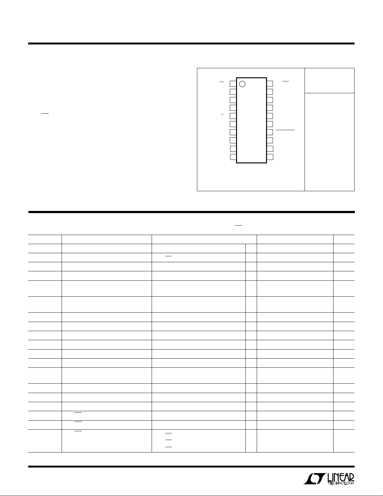
VIN = 5V
VIN = 5V
VIN = 3.3V
VIN = 3.3V
D1 = MBR0530
D1 = 4 BAT54Cs
IN PARALLEL
Micropower Step-Up
DC/DC Converter for
PCMCIA Card Flash Memory
EATU
F
■
60mA Output Current at 12V from 3V Supply
■
Shutdown to 10µA
■
Programmable 12V or 5V Output
■
Up to 85% Efficiency
■
Quiescent Current: 750µA
■
Low V
■
Uses Low Value, Thin, Surface Mount Inductors
■
Ultra-Thin 20-Lead TSSOP Package
PPLICATI
A
■
PCMCIA Card Flash Memory VPP Generator
■
Portable Computers
■
Portable Instruments
■
DC/DC Converter Module Replacements
S
RE
Switch: 300mV at 0.5A Typical
CESAT
U
O
S
DUESCRIPTIO
The LT®1106 is the industry’s first DC/DC converter
designed for use on Type I and Type II PCMCIA cards. The
device senses the VPP1 and VPP2 lines at the PCMCIA
socket and generates a regulated 12V, 60mA programming supply if the socket does not provide it. Internal logic
simplifies the interface to PCMCIA card microcontrollers.
One input selects a 12V or 5V regulated output, while
another input controls micropower shutdown. Two logic
outputs indicate when the selected programming voltage
is valid and whether the input supply is 3.3V or 5V.
The regulator features Burst ModeTM operation with a 0.5A,
300mV switch for efficiency up to 85%. High frequency
500kHz switching permits the use of small value, flat
inductors that fit neatly on PCMCIA cards. The device
requires just 1µF of output capacitance.
Quiescent current is 750µA which drops to 350µA when
the card runs off the socket supply. The shutdown pin
reduces supply current to only 10µ A. The device includes
a soft start feature which limits supply current transients
when the card is inserted into a hot socket.
, LTC and LT are registered trademarks of Linear Technology Corporation.
Burst Mode is a trademark of Linear Technology Corporation.
V
CC
3.3V/5V
+
VPP1
VPP2
DALE ILS-3825-01 OR
*
COILTRONICS CTX02-11238-3
MOTOROLA MBR0530
**
U
O
A
PPLICATITYPICAL
12V, 60mA Flash Memory Programming Supply
4.7µF
TANT
ALUM
0.1µF
0.1µF
POWER ON
D
BSS84
S
0.1µF
BSS84
L1*
10µH
V
CC
VPP1
D
G1
LT1106
S
VPP2
G2
ON/OFF
VPP VALID
3/5 DETECT
SOFT START
GNDPGND
SW
AVPP
12/5
D1**
1M 0.1µF
1µF
470pF
LT1106 • TA01
12V Output Efficiency
12V/60mA
VPP VALID
3/5
1
Page 2
LT1106
A
W
O
LUTEXI T
S
A
WUW
ARB
U
G
I
S
VCC Voltage............................................................... 7V
VSW Voltage............................................................ 20V
AVPP Voltage ......................................................... 20V
VPP1, VPP2 Voltage ............................................... 20V
G1, G2 Voltage ....................................................... 20V
V
V
I
LIM
Voltage......................................................... 7V
ON/OFF
Voltage ............................................................. 7V
SEL
Voltage .............................................................. 7V
Maximum Power Dissipation ............................ 500mW
Operating Temperature Range ..................... 0°C to 70°C
Storage Temperature Range ................. – 65°C to 150°C
Lead Temperature (Soldering, 10 sec).................. 300°C
LECTRICAL C CHARA TERIST
E
ICS
TA = 25°C, VCC = 5V, V
/
PACKAGE
SELECT 12/5
SOFT START
V
CC
V
CC
3/5
PGND
PGND
NC
V
SW
V
SW
T
Consult factory for Industrial and Military grade parts
O
RDER I FOR ATIO
TOP VIEW
1
2
3
4
5
6
7
8
9
10
F PACKAGE
20-LEAD PLASTIC TSSOP
= 100°C, θJA = 90°C/W
JMAX
= 3V, unless otherwise noted.
ON/OFF
20
19
18
17
16
15
14
13
12
11
ON/OFF
AVPP
VPP1
VPP2
G1
G2
VPP VALID
GND
NC
V
SW
WU
ORDER PART
NUMBER
LT1106CF
U
SYMBOL PARAMETER CONDITIONS MIN TYP MAX UNITS
I
Q
f
OSC
DC Maximum Duty Cycle ● 80 85 92 %
t
ON
V
CESAT
Quiescent Current V
Quiescent Current, Shutdown V
“Doze” Mode Current V
Input Voltage Range 2 6 V
Output Sense Voltage V
Output Referred V
Comparator Hysteresis V
Oscillator Frequency Current Limit Not Asserted 400 500 700 kHz
Switch On-Time 1.7 µs
Reference Line Regulation 2V < VIN < 6V 0.06 0.15 %/V
Switch Saturation Voltage ISW = 0.5A 230 350 mV
Switch Leakage Current VSW = 12V, Switch Off 0.1 10 µA
Switch Current Limit VIN = 5V, Soft Start Floating 450 600 900 mA
Soft Start Pin Current Soft Start Grounded 80 120 µA
Select Input Voltage Low 0.8 V
Select Input Voltage High 1.6 V
ON/OFF Input Voltage Low 0.8 V
ON/OFF Input Voltage High 1.6 V
ON/OFF Bias Current V
= 0.2V, AVPP = 12V 750 900 µA
SEL
= 0.2V 9 15 µA
ON/OFF
= 0.2V, VPP1 or VPP2 = 12V 320 µA
SEL
= 3V, VPP1 and VPP2 Floating ● 4.75 5 5.25 V
SEL
= 0.2V, VPP1 and VPP2 Floating ● 11.50 12 12.60 V
V
SEL
= 3V 15 mV
SEL
= 0.2V 35 mV
SEL
= 3V, Soft Start Floating 500 650 950 mA
V
IN
= 5V 16.0 24.0 µA
ON/OFF
= 3V 8.0 14.0 µA
V
ON/OFF
= 0V 0.1 1.1 µA
V
ON/OFF
2
Page 3
LT1106
LECTRICAL C CHARA TERIST
E
ICS
TA = 25°C, VCC = 5V, V
= 3V, unless otherwise noted.
ON/OFF
SYMBOL PARAMETER CONDITIONS MIN TYP MAX UNITS
Select Pin Bias Current 0V < V
< 5V 0.1 1 µA
SEL
VPP1/VPP2 Input Sense Threshold 11.0 11.5 11.9 V
AVPP Pin Input Current 50 90 µA
= 0.2V 0.1 1 µA
V
ON/OFF
VPP1/VPP2 Pin Input Current 50 90 µA
= 0.2V 0.1 1 µA
V
ON/OFF
VPP VALID Threshold AVPP Rising (High to Low Transition) ● 11.4 12 V
VPP VALID Output Voltage Low I
VPP VALID Output Voltage High I
= 100µA 0.13 0.3 V
SINK
= 2.5µA 4 4.5 V
SOURCE
3/5 Comparator Threshold ● 3.6 3.75 4.2 V
3/5 Comparator Output High I
3/5 Comparator Output Low I
= 50µA 3.65 3.8 V
LOAD
= 50µA 0.75 0.9 V
LOAD
Off State Current at G1/G2 VPP1 = 10V, VG1 = 12V or VPP2 = 10V, 0.1 1 µA
VG2 = 12V or V
ON/OFF
= 0V
The ● denotes specifications which apply over the full operating
temperature range.
W
U
TYPICAL PERFORMANCE CHARACTERISTICS
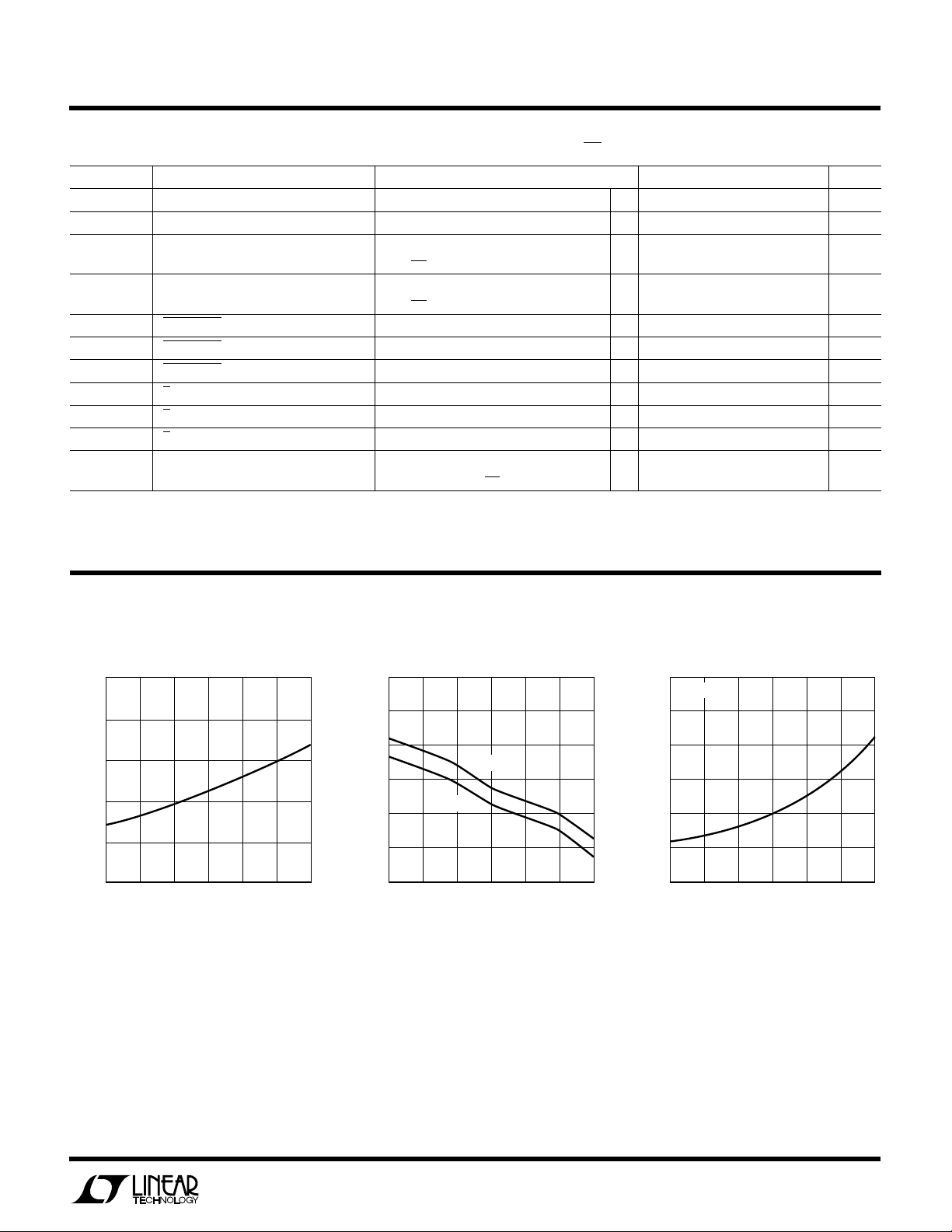
Oscillator Frequency Switch Current Limit Switch Saturation Voltage
800
700
600
500
400
OSCILLATOR FREQUENCY (kHz)
300
–50
02550
–25
TEMPERATURE (°C)
75 100
LT1106 • TPC01
1000
900
800
700
600
SWITCH CURRENT (mA)
500
400
–50
VCC = 5V
02550
–25
TEMPERATURE (°C)
VCC = 3V
75 100
LT1106 • TPC02
250
ISW = 500mA
225
200
175
150
125
SWITCH SATURATION VOLTAGE (mV)
100
–50
02550
–25
TEMPERATURE (°C)
75 100
LT1106 • TPC03
3
Page 4

LT1106
TEMPERATURE (°C)
–50
4.80
AVPP SENSE VOLTAGE (V)
4.85
4.90
4.95
5.00
5.10
–25
02550
LT1106 • TPC06
75 100
5.05
12/5 SELECT = 1
TEMPERATURE (°C)
–50
70
MAXIMUM DUTY CYCLE (%)
75
80
85
90
95
–25
02550
LT1106 • TPC09
75 100
W
U
TYPICAL PERFORMANCE CHARACTERISTICS
3/5 Comparator Threshold AVPP Sense Voltage AVPP Sense Voltage
4.00
3.95
3.90
12.20
12.15
12.10
12.05
12/5 SELECT = 0
3.85
3.80
THRESHOLD VOLTAGE (V)
3.75
3.70
–50
02550
–25
TEMPERATURE (°C)
Supply Current in Shutdown
14
12
10
8
6
4
SUPPLY CURRENT (µA)
2
0
–50
–25 0
VCC = 5V
VCC = 3V
TEMPERATURE (°C)
LT1106 • TPC04
50 100
25 75
LT1106 • TPC07
75 100
12.00
11.95
11.90
AVPP SENSE VOLTAGE (V)
11.85
11.80
–25 0 50
–50
TEMPERATURE (°C)
Supply Current
800
700
600
500
SUPPLY CURRENT (µA)
400
300
–50
02550
–25
TEMPERATURE (°C)
25
VCC = 5V
V
= 3V
CC
75
LT1106 • TPC05
75 100
LT1106 • TPC08
100
Maximum Duty Cycle
Start-Up Waveforms, I
12V
VAVPP
2V/DIV
VPP VALID
10V/DIV
ON/OFF
10V/DIV
4
50µs/DIV
LOAD
= 1mA
LT1106 • TPC10
V
OUT
5V/DIV
500mA/DIV
V
ON/OFF
10V/DIV
Start-Up Waveforms with Soft
Start, I
I
L
LOAD
= 10mA
50µs/DIV
LT1106 • TPC11
12V OUTPUT
1V/DIV
AC COUPLED
60mA
I
LOAD
10mA
Load Transient Response,
C
= 1µF
OUT
50µs/DIV
LT1106 • TPC12
Page 5

UU U
PI FU CTIO S
LT1106
SELECT 12/5 (Pin 1): Tie to VIN or logic 1 for 5V output;
tie to GND or logic 0 for 12V output.
SOFT START (Pin 2): A 0.1µ F/1MΩ parallel RC from this
pin to GND provides a Soft Start function upon device
turn-on. Initially about 80µ A will flow from the pin into the
capacitor. When the voltage at the pin reaches approximately 0.4V, current ceases flowing out of the pin. See
Applications Information section.
VCC (Pins 3, 4): Input Supply. Both pins should be tied
together. At least 1µF input bypass capacitance is re-
quired. More capacitance reduces ringing on the supply
line.
3/5 (Pin 5): Supply Comparator Output. This pin provides
logic output indicating the value of the input supply. High
when VCC = 5V; low when VCC = 3.3V.
PGND (Pins 6, 7): Power Ground. Connect to ground plane.
VSW (Pins 9, 10, 11): Collector of Power Switch. High dV/
dt present on this pin. To minimize radiated noise keep
layout short and direct.
GND (Pin 13): Signal Ground. Connect of ground plane.
VPP VALID (Pin 14): This pin provides a logic signal
indicating that ouput voltage is greater than 11.4V. Active
low with internal 200k pull-up resistor.
G1, G2 (Pins 16, 15): External MOSFET Gate Drives. When
VPP1 or VPP2 is greater than 11.7V, G1 or G2 is driven to
about 0.8V. When VPP1 or VPP2 is less than 11.7V, the
drives assume a high impedance state pulled up to the
AVPP pin through an internal 100k resistor.
VPP1, VPP2 (Pins 18, 17): Programming Power Inputs.
The LT1106 senses both VPP1 and VPP2 supplies at the
PCMCIA card socket. If VPP1 or VPP2 is greater than 11V,
the LT1106 operates in “Doze” Mode—the switching
regulator turns off and the drive to external P-channel
MOSFETs turns on. Supply current in Doze Mode is about
350µ A. Input current into VPP1 and VPP2 is about 1µA
when the device is shut down.
AVPP (Pin 19): Output Sense Pin. This pin connects to a
1MΩ resistive divider that sets the output voltage. In
shutdown, the resistor string is disconnected and current
into this pin is reduced to <1µA.
ON/OFF (Pin 20): Shutdown Control. When pulled below
1.5V, this pin disables the LT1106 and reduces supply
current to 10µA. All circuitry except the 3/5 comparator
is disabled in shutdown. The part is enabled when
ON/OFF is greater than 1.5V.
5
Page 6

LT1106
BLOCK DIAGRA
12/5
SELECT
191
W
VPP2
VPP1AVPP
18
ON/0FF
17
20
G1
G2
16
15
565k
299k
4k
100k
BIAS
–
+
–
+
V
V
REF
+
C2
CC
200k
VPP VALID
14
36mV
+
–
+
C3
–
Q3
R2
700Ω
BIAS
V
3,4
CC
R1
3Ω
–
2
–
C1
+
V
CC
V
1.24V
REF
3.7V
+
–
OFF
500kHz
OSCILLATOR
5
3/5
SOFT START
13
GND
Q2
1×
SW
9,10,11
Q1
50×
6,7
PGND
LT1106 • BD
U
WUU
APPLICATIONS INFORMATION
Functional Description
The LT1106 is a micropower, step-up DC/DC converter
specifically configured for PCMCIA flash memory card
VPP generation. The device generates a 5V or 12V output
selectable via the 12/5 Select pin. If 12V is present on
either the VPP1 or VPP2 pins, gate drive outputs G1 and
G2 are driven low, turning on external PMOS devices. The
switching regulator inside the LT1106 is idled when 12V
is present on VPP1 or VPP2.
The VPP VALID output goes low when the voltage at AVPP
exceeds 11.4V This signal can be used to indicate presence of a valid programming voltage. The 3/5 comparator
indicates whether the input voltage is 3.3V or 5V.
6
The Soft Start pin can be used to limit inrush current upon
start-up. A 0.1µ F capacitor in parallel with a 1M resistor is
connected between this pin and ground to limit peak
inductor current at start-up.
Switching Regulator Operation
When 12V is not present on the VPP1 or VPP2 pins and the
device is enabled (ON/OFF = 1), the LT1106 generates a
regulated voltage at the AVPP pin. This voltage is programmable between 5V or 12V depending on the state of
the 12/5 Select pin. Referring to the block diagram, hysteretic comparator C1 monitors AVPP via the resistor divider.
When the negative input of C2 falls below 1.24V, C1’s
Page 7

LT1106
U
WUU
APPLICATIONS INFORMATION
output goes high, enabling the oscillator. Switch Q1
alternately turns on causing current build-up in the inductor; then turns off allowing the built-up current to flow into
the output capacitor via the catch diode. As the output
voltage increases, so does the voltage at C1’s negative
input. When it exceeds the reference voltage plus C1’s
hysteresis, C1 turns the oscillator off.
Switch current is limited to approximately 600mA by Q2,
R1 and C3. Two percent of Q1’s collector current flows in
Q2; this current flows through R1 causing a voltage drop
in R1 proportional to Q1’s collector current. When R1’s
drop equals 36mV, comparator C3 forces the oscillator
off. This action results in varying on-time, fixed off-time
operation that keeps peak switch current controlled. By
connecting a 0.1µF capacitor from the Soft Start pin to
ground, a current will flow in Q3 upon start-up. The current
flows through 700Ω resistor R2, reducing the amount of
current needed from Q2 to force the oscillator off. As
current flows into the 0.1µ F capacitor, the voltage at pin 2
increases and eventually current ceases to flow in Q3.
Inductor Selection
All components for use in PCMCIA Type I cards must be
less than 1.1mm high. This somewhat limits the selection
of appropriate inductors. Dale Electronics (605-665-9301)
manufactures the ILS-3825-01, a monolithic ferrite inductor that meets Type I height requirements. Generally,
inductors used with the LT1106 must fulfill several requirements. It must be able to carry 0.95A (the maximum
switch current) without saturation. DCR should be kept
low to maintain efficiency. The switching frequency of the
LT1106 is quite high, over 500kHz so magnetic material is
important. Ferrite core material works well in this frequency range. Avoid low cost iron powder cores which
have substantial AC loss at the LT1106’s switching frequency. Inductance value need not be over 10µH.
Capacitor Selection
The LT1106 will operate with 1µ F of output capacitance.
Output ripple voltage is approximately 400mV with this
value and can be reduced significantly by increasing
output capacitance. The ripple voltage, although on the
high side, poses no problems for programming flash
memory. If operating the device in 5V ouput mode the
capacitance should be increased. Ceramic capacitors are
suitable for the output. Distributed capacitance, i.e.,
0.1µF or 0.2µF units next to individual flash memory
chips, is acceptable. The input capacitor should have at
least some tantalum capacitance (low Q) to minimize
resonance on the input. Flash memory cards are typically
several inches away from a solid low impedance supply
due to sockets, connectors, etc. If just ceramic capacitors are used at the supply pin of the LT1106, switching
currents will resonate the supply line causing ringing that
can exceed 500mV
ceramic capacitors causes this. A few microfarad’s worth
of tantalum capacitors with moderate ESR and low Q
characteristics will reduce or eliminate the problem.
Diode Selection
As with inductors, most good power Schottky diodes are
in packages that exceed the 1.1mm height limit of the
Type I PCMCIA card. Motorola manufactures the MBRO530
Schottky diode, ideal for use with the LT1106. This
diode’s maximum height however, is 1.35mm, making it
difficult to use in Type 1 cards. Philips Components
manufactures the BAT54C. Four units in parallel make an
adequate diode.
. The high Q, low ESR nature of
P-P
Information furnished by Linear Technology Corporation is believed to be accurate and reliable.
However, no responsibility is assumed for its use. Linear Technology Corporation makes no representation that the interconnection of its circuits as described herein will not infringe on existing patent rights.
7
Page 8

LT1106
TYPICAL APPLICATION
Alternative Scheme Allows 12V from VPP1/VPP2 to Provide Power When LT1106 is in Shutdown
V
CC
3.3V/5V
+
U
4.7µF
D**
VPP1
D**
VPP2
L1*
10µH
V
CC
SW
LT1106
VPP VALID
AVPP
D**
12V/60mA
1µF
VPP VALID
470pF
POWER ON
ON/OFF
DALE ILS-3824-01
*
MBR0530 OR 4 BAT54s IN PARALLEL
**
U
PACKAGE DESCRIPTION
0.169 – 0.176*
(4.30 – 4.48)
0° – 8°
0.004 – 0.071
(0.09 – 0.18)
*THESE DIMENSIONS DO NOT INCLUDE MOLD FLASH OR PROTRUSIONS.
MOLD FLASH OR PROTRUSIONS SHALL NOT EXCEED 0.006 INCH (0.15mm).
0.020 – 0.028
(0.50 – 0.70)
Dimensions in inches (millimeters) unless otherwise noted.
0.0256
(0.65)
BSC
SOFT START
GND
SELPGND
1M 0.1µF
F Package
20-Lead Plastic TSSOP
0.007 – 0.012
(0.18 – 0.30)
LT1106 • TA03
0.043
(1.10)
MAX
0.002 – 0.006
(0.05 – 0.15)
0.252 – 0.260*
(6.40 – 6.60)
20 19 18 17 16 15
111214 13
0.246 – 0.256
(6.25 – 6.50)
RELATED PARTS
PART NUMBER DESCRIPTION COMMENTS
LT1109 5V to 12V/60mA VPP Generator 300µA IQ, 120kHz Oscillator
LT1109A 5V to 12V/120mA VPP Generator 300µA IQ, 120kHz Oscillator
LT1301 5V to 12V/200mA VPP Generator 120µA IQ, 155kHz Oscillator
LT1309 5V to 12V/60mA VPP Generator 650µA IQ, 650kHz Oscillator
Linear Technology Corporation
8
1630 McCarthy Blvd., Milpitas, CA 95035-7487
(408) 432-1900
●
FAX
: (408) 434-0507
●
TELEX
: 499-3977
7
6
F20 TSSOP 0395
8910
134
2
5
LT/GP 0595 10K • PRINTED IN THE USA
LINEAR TECHNOLOGY CORPORATION 1995
 Loading...