

Datasheet LT1105IN8, LT1105IN, LT1105CN8, LT1105CN, LT1103CT7 Datasheet (Linear Technology)
Page 1

OBSOLETE:
FOR INFORMATION PURPOSES ONLY
Contact Linear Technology for Potential Replacement
FEATURES
■
±1% Line and Load Regulation with No Optocoupler
■
Switch Frequency Up to 200kHz
■
Internal 2A Switch and Current Sense (LT1103)
■
Internal 1A Totem-Pole Driver (LT1105)
■
Start-Up Mode Draws Only 200µA
■
Fully Protected Against Overloads
■
Overvoltage Lockout of Main Supply
■
Protected Against Underdrive or Overdrive to FET
■
Operates in Continuous or Discontinuous Mode
■
Ideal for Flyback and Forward Topologies
■
Isolated Flyback Mode Has Fully Floating Outputs
U
APPLICATIONS
■
Up to 250W Isolated Mains Converter
■
Up to 50W Isolated Telecom Converter
■
Fully Isolated Multiple Outputs
■
Distributed Power Conversion Networks
LT1103/LT1105
Offline Switching Regulator
U
DESCRIPTION
The LT®1103 Offline Switching Regulator is designed for
high input voltage applications using an external FET
switch whose source is driven by the open collector output
of the LT1103. The LT1103 is optimized for 15W to 100W
applications. For higher power applications or additional
switch current flexibility, the LT1105 is available and its
totem pole output drives the gate of an external FET.
Unique design of the LT1103/LT1105 eliminates the need
for an optocoupler while still providing ±1% load and line
regulation in a magnetic flux-sensed converter. This significantly simplifies the design of offline power supplies
and reduces the number of components which must cross
the isolation barrier to one, the transformer.
The LT1103/LT1105 current mode switching techniques
are well suited to transformer isolated flyback and forward
topologies while providing ease of frequency compensation with a minimum of external components. Low external part count for a typical application combines with a
, LTC and LT are registered trademarks of Linear Technology Corporation.
TYPICAL APPLICATION
Fully Isolated Flyback 100kHz 50W Converter with Load Regulation Compensation
85V
TO 270V
AC
AC
+
–
BRIDGE
RECTIFIER
+
LINE
FILTER
+
220µF
385V
BAV21
13k
1%
4.75k
1%
499Ω
1000pF
18.7k
0.047µF
100Ω
BAV21
1N4148
Danger!! Lethal Voltages Present – See Text
39µF
35V
+
220k
1W
0.047µF
V
FB
GND
IN
U
DANGER!!
HIGH VOLTA
1N4148
V
SW
LT1103
15V
V
OSC
C
330Ω
0.1µF
G
390pF
E!!
1.5KE300A
5W
MUR150
BUK426-800A
10Ω
+
1µF
25V
OPTIONAL OUTPUT FILTER
MBR2045
*OUTPUT CAPACITOR IS THREE 1200µF,
50V CAPACITORS IN PARALLEL TO
ACHIEVE REQUIRED RIPPLE CURRENT
RATING AND LOW ESR.
TRANSFORMER DATA:
COILTRONICS CTX110228-3
L
= 1.6mH
(PRI)
N
PRI:NSEC
N
BIAS:NSEC
LT1103 TA13
+
*50V
3600µF
WINDINGS FOR
OPTIONAL
OUTPUTS
±12V
DC
= 1:0.05
= 1:0.27
10µH
+
50V
470µF
5V
10A
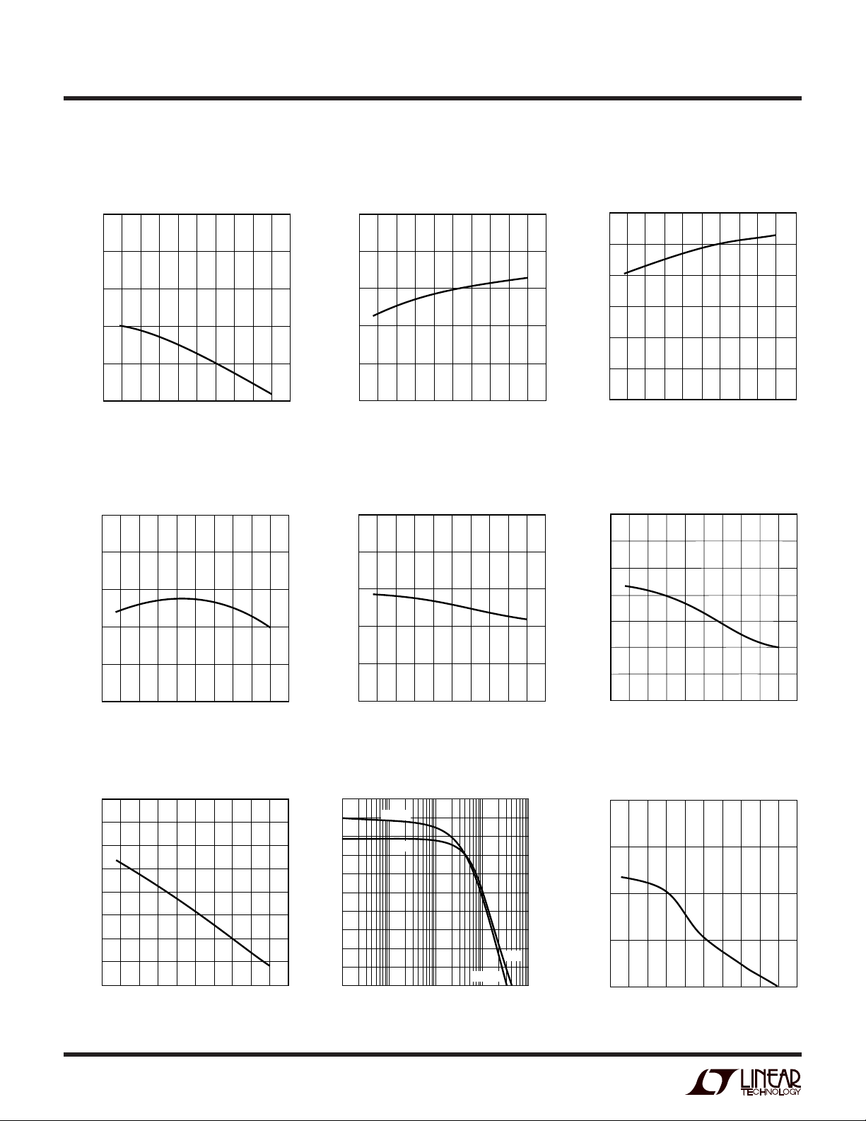
Load Regulation
5.25
5.20
5.15
5.10
5.05
(V)
5.00
OUT
V
4.95
4.90
4.85
4.80
4.75
0
270V
2
3
1
220V
AC
110V
AC
AC
579
6
4
I
OUT
8
(A)
85V
AC
LT1103 TA02
10
1
Page 2

LT1103/LT1105
U
DESCRIPTION
200kHz maximum switching frequency to achieve high
power density. Performance at switching frequencies
above 100kHz may be degraded due to internal timing
constraints associated with fully isolated flyback mode.
Included are the oscillator, control, and protection circuitry such as current limit and overvoltage lockout.
Switch frequency and maximum duty cycle are adjustable.
Bootstrap circuitry draws 200µA for start-up of isolated
topologies. A 5V reference as well as a 15V gate bias are
available to power external primary-side circuitry. No
external current sense resistor is necessary with LT1103
because it is integrated with the high current switch. The
LT1105 brings out the input to the current limit amplifier
and requires the use of an external sense resistor.
The LT1103/LT1105 have unique features not found on
other offline switching regulators. Adaptive antisat switch
drive allows wide ranging load currents while maintaining
high efficiency. The external FET is protected from insufficient or excessive gate drive voltage with a drive detection circuit. An externally activated shutdown mode
reduces total supply current to less than 200µA, typical for
standby operation. Fully isolated and regulated outputs
can be generated in the optional isolated flyback mode
without the need for optocouplers or other isolated feedback paths.
U
U
WAR I G!
DANGEROUS AND LETHAL POTENTIALS ARE
PRESENT IN OFFLINE CIRCUITS!
BEFORE PROCEEDING ANY FURTHER, THE
READER IS WARNED THAT CAUTION MUST
BE USED IN THE CONSTRUCTION, TESTING
AND USE OF OFFLINE CIRCUITS. HIGH
VOLTAGE, AC LINE-CONNECTED POTENTIALS
ARE PRESENT IN THESE CIRCUITS. EXTREME
CAUTION MUST BE USED IN WORKING WITH
AND MAKING CONNECTIONS TO THESE
CIRCUITS. REPEAT: OFFLINE CIRCUITS
CONTAIN DANGEROUS, AC LINE-CONNECTED
HIGH VOLTAGE POTENTIALS. USE CAUTION.
ALL TESTING PERFORMED ON AN OFFLINE
CIRCUIT MUST BE DONE WITH AN ISOLATION
TRANSFORMER CONNECTED BETWEEN THE
OFFLINE CIRCUIT'S INPUT AND THE AC LINE.
USERS AND CONSTRUCTORS OF OFFLINE
CIRCUITS MUST OBSERVE THIS PRECAUTION
WHEN CONNECTING TEST EQUIPMENT TO
THE CIRCUIT TO AVOID ELECTRIC SHOCK.
REPEAT: AN ISOLATION TRANSFORMER
MUST BE CONNECTED BETWEEN THE CIRCUIT
INPUT AND THE AC LINE IF ANY TEST
EQUIPMENT IS TO BE CONNECTED.
WW
W
ABSOLUTE MAXIMUM RATINGS
VIN.......................................................................... 30V
V
Output Voltage (LT1103)................................. 50V
SW
VSW Output Current (200ns)(LT1105) ................. ±1.5A
VC, FB, OSC, SS ........................................................ 6V
I
(LT1105) ........................................................... 3V
LIM
0VLO Input Current ............................................... 1mA
Lead Temperature (Soldering, 10 sec.)................ 300°C
U
(Note 1)
2
Maximum Operating Ambient Temperature Range
LT1103C .............................................. 0°C to 70°C
LT1105C .............................................. 0°C to 70°C
Maximum Operating Junction Temperature Range
LT1103C ............................................. 0°C to 100°C
LT1105C ............................................ 0°C to 100°C
LT1105I ......................................... –40°C to 125°C
Storage Temperature Range ................. –65°C to 150°C
Page 3
LT1103/LT1105
U
W
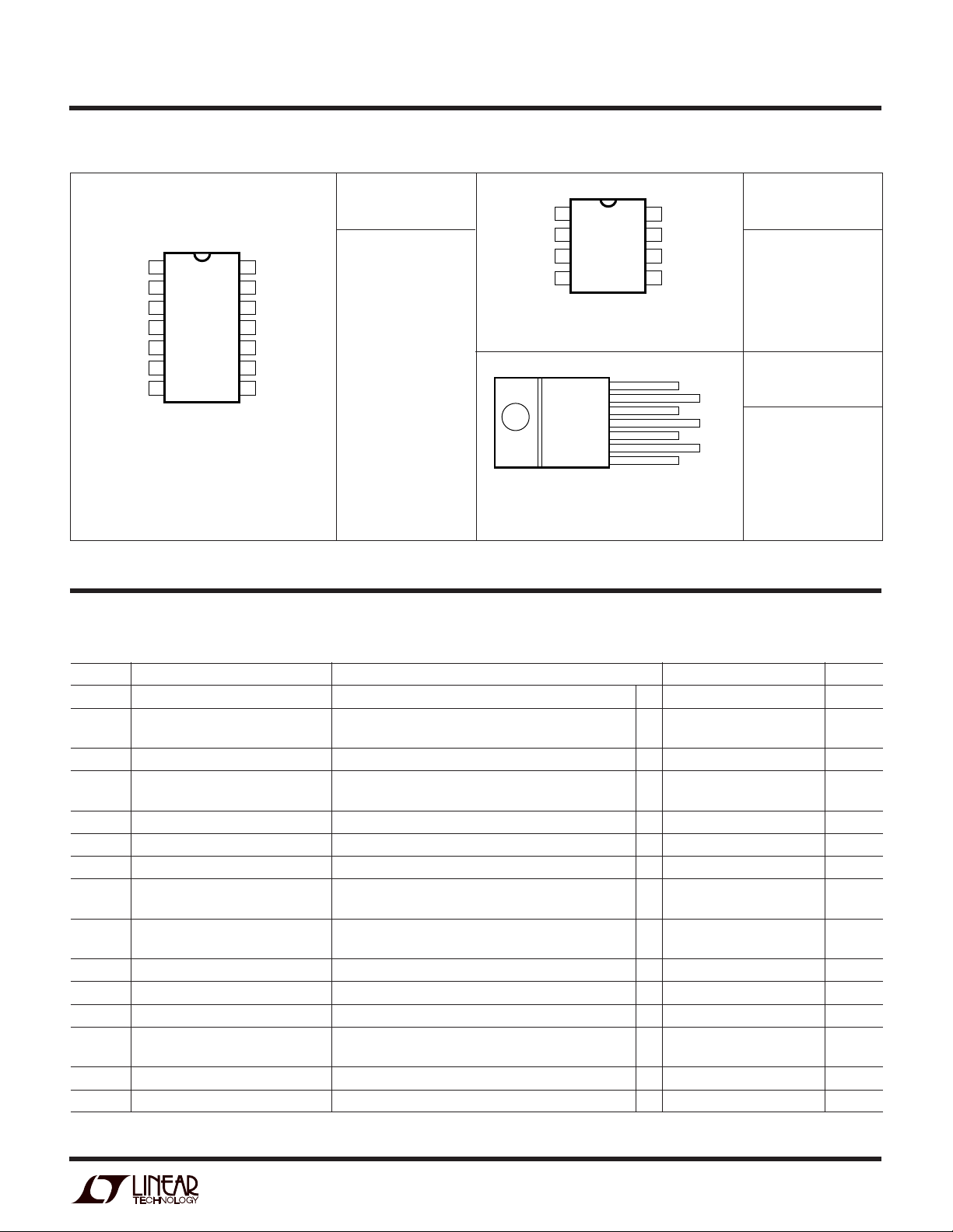
PACKAGE/ORDER INFORMATION
ORDER PART
NUMBER
TOP VIEW
PWRGND
1
2
OVLO
3
FB
4
V
C
5
5V
6
SS
7
GND
N PACKAGE
14-LEAD PDIP
PINS 1 AND 7 MUST BE TIED TOGETHER
T
= 100°C, θJA = 100°C/W
JMAX
V
14
SW
NC
13
NC
12
15V
11
V
10
IN
OSC
9
I
8
LIM
Consult factory for Military grade parts.
LT1105CN
LT1105IN
U
TOP VIEW
GND
1
I
2
LIM
3
FB
45
V
C
N8 PACKAGE
8-LEAD PDIP
T
= 100°C, θJA = 130°C/W
JMAX
FRONT VIEW
7
6
5
4
3
2
1
T7 PACKAGE
CASE IS CONNECTED TO GROUND. LEADS ARE FORMED
7-LEAD TO-220
= 100°C, θJA = 50°C/W
T
JMAX
ORDER PART
8
V
SW
15V
7
6
V
IN
OSC
NUMBER
LT1105CN8
LT1105IN8
ORDER PART
15V
V
IN
OSC
GND
V
C
FB
V
SW
NUMBER
LT1103CT7
ELECTRICAL CHARACTERISTICS
VIN = 20V, VC = 0.85V, OVLO = 0V, VSW Open, TA = 25°C, unless otherwise noted.
SYMBOL PARAMETER CONDITIONS MIN TYP MAX UNITS
I
Q
I
START
V
REF
V
GATE
SF Oscillator Scaling Factor FB = 4V, VC = Open, Measured at VSW, ISW = 25mA, 36 40 44 Hz • µF
Supply Current 8V < VIN < 30V, After Device Has Started ● 10 20 30 mA
Start-Up Current VIN < VIN Start Threshold ● 200 400 µA
Industrial Grade
● 450 µA
VIN Start Threshold ● 14.5 16.0 17.5 V
VIN Shutdown Threshold Note: Switching Stops When VSW < 10V (LT1103) ● 5.0 7.0 8.0 V
Note: Switching Stops When V
< 10V (LT1105)
GATE
5V Reference Voltage ● 4.80 4.95 5.20 V
V
Line Regulation 10V < VIN < 30V ● 0.025 0.1 %/ V
REF
V
Load Regulation 0mA < IL < 20mA ● 0.025 0.05 %/mA
REF
V
Short-Circuit Current Commercial Grade ● 25 60 110 mA
REF
Industrial Grade
● 20 120 mA
15V Short-Circuit Current Commercial Grade ● 30 130 mA
Industrial Grade
● 25 140 mA
15V Gate Bias Reference 17 < VIN < 30V, 0mA < IL < 30mA ● 13.8 15.0 16.2 V
15V Dropout Voltage VIN = 15V, IL = 30mA ● 2.0 2.5 V
15V Short-Circuit Current ● 30 70 130 mA
OVLO = 5V, f
OSC
= SF/C
OSC,
40kHz < f
< 200kHz ● 32 40 48 Hz • µF
OSC
Oscillator Valley Voltage 2.0 V
Oscillator Peak Voltage 4.5 V
3
Page 4

LT1103/LT1105
ELECTRICAL CHARACTERISTICS
VIN = 20V, VC = 0.85V, OVLO = 0V, VSW Open, TA = 25°C, unless otherwise noted.
SYMBOL PARAMETER CONDITONS MIN TYP MAX UNIT
DC Preset Max Switch Duty Cycle FB = 4V, VC = Open, f
(LT1103) Note: Maximum Duty Cycle Can Be Altered at OSC Pin
Preset Max Switch Duty Cycle FB = 4V, VC = Open, f
(LT1105) Note: Maximum Duty Cycle Can Be Altered at OSC Pin
Industrial Grade ● 55 75 %
OVLO Threshold Overvoltage Lockout Threshold at Which Switching is Inhibited ● 2.3 2.5 2.7 V
Industrial Grade
OVLO Input Bias Current OVLO = 2V, Measured Out of Pin (Note 2) ● 1.0 3.0 µA
V
FB
gm Error Amp Transconductance ∆I(VC) = ±50µA 9000 12000 17500 µmho
A
V
BV Switch Breakdown Voltage ISW = 5mA ● 50 70 V
∆I
IN
∆I
SW
FB Threshold Voltage I(VC) = 0mA 4.425 4.50 4.575 V
FB Input Bias Current FB = VFB (Note 3) ● 51020 µA
Industrial Grade
Change in FB Input FB = VFB, VC = 1V to 4V (Note 3) 8 11 13 µA/V
Bias Current with Change in V
FB Threshold Line Regulation 10V < VIN < 30V ● 0.025 0.10 %/V
Error Amp Voltage Gain 1V < VC < 3V ● 500 1250 V/V
VC Switching Threshold Switch Duty Cycle = 0% ● 0.85 1.25 1.4 V
Shutdown Threshold Voltage ● 50 150 250 mV
Error Amp Source Current ● 150 275 µA
Error Amp Sink Current ● 1.5 3 4.5 mA
Error Amp Clamp Voltage FB = 4.75V ● 0.3 0.7 0.9 V
Soft-Start Charging Current SS = 0V ● 25 40 60 µA
Soft-Start Reset Current VIN = 6V, SS = 0.3V ● 12 mA
Output Switch Leakage VSW = 45V ● 500 µA
(LT1103) V
(LT1103)
VSW Current Limit (LT1103) Duty Cycle = 25% (Note 4) ● 2.0 2.5 3.0 A
Output Switch On Resistance ● 0.4 0.75 Ω
(LT1103)
IQ Increase During Switch On Time ISW = 0.5A to 1.5A ● 30 50 mA/A
(LT1103)
Switch Output High Level ISW = 200mA, V
(LT1105) I
Switch Output High Level I
Industrial Grade I
C
Industrial Grade
Industrial Grade
Industrial Grade
Industrial Grade
Industrial Grade
FB = 4.0V
Industrial Grade
= 15V ● 200 µA
SW
= 750mA, V
SW
= 200mA, V
SW
= 750mA, V
SW
= 40kHz, ISW = 25mA, ● 58 65 72 %
OSC
= 40kHz, ISW = 25mA, ● 56 63 70 %
OSC
● 2.2 2.8 V
● 4.400 4.50 4.600 V
● 422µA
● 71114 µA/V
● 615µA/V
● 6000 12000 20000 µmho
● 5000 24000 µmho
● 450 V/V
● 50 300 mV
● 0.7 4.5 mA
● 4.2 4.4 4.6 V
● 20 75 µA
= 15V ● 13.00 13.5 V
GATE
= 15V ● 12.50 13.2 V
GATE
= 15V ● 12.75 V
GATE
= 15V ● 12.25 V
GATE
4
Page 5
LT1103/LT1105
ELECTRICAL CHARACTERISTICS
VIN = 20V, VC = 0.85V, OVLO = 0V, VSW Open, TA = 25°C, unless otherwise noted.
SYMBOL PARAMETER CONDITONS MIN TYP MAX UNIT
Switch Output Low Level ISW = 200mA ● 0.25 0.50 V
(LT1105) I
Rise Time (LT1105) CL = 1000pF 50 ns
Fall Time (LT1105) CL = 1000pF 20 ns
I
Threshold Voltage (LT1105) Duty Cycle = 25% (Note 5) ● 300 375 450 mV
LIM
Low Switch Drive Lockout Measured at VSW (LT1103) ● 9.0 9.5 10.5 V
Threshold Measured at 15V Gate Bias Reference (LT1105)
High Switch Drive Lockout Measured at VSW (LT1103) ● 17.0 18.5 20.0 V
Threshold Measured at 15V Gate Bias Reference (LT1105)
= 750mA ● 0.75 1.50 V
SW
The ● denotes specifications which apply over the full operating
temperature range.
Note 1: Absolute Maximum Ratings are those values beyond which the life
of a device may be impaired.
Note 2: The OVLO pin is clamped with a 5.5V Zener and can sink a
maximum input current of 1mA.
Note 3: FB input bias current changes as a function of the V
Rate of change of FB input bias current is 11µA/V of change on V
pin voltage.
C
. By
C
Note 4: Current limit on VSW is constant for DC < 35% and decreases for
DC > 35% due to internal slope compensation circuity. The LT1103 switch
current limit is given by I
Note 5: The current limit threshold voltage is constant for DC < 35% and
decreases for DC > 35% due to internal slope compensation circuitry. The
LT1105 switch current limit threshold voltage is given by V
(1.7 – DC) above 35% duty cycle.
including a resistor in series with the FB pin, load regulation can be set
to zero.
W
U
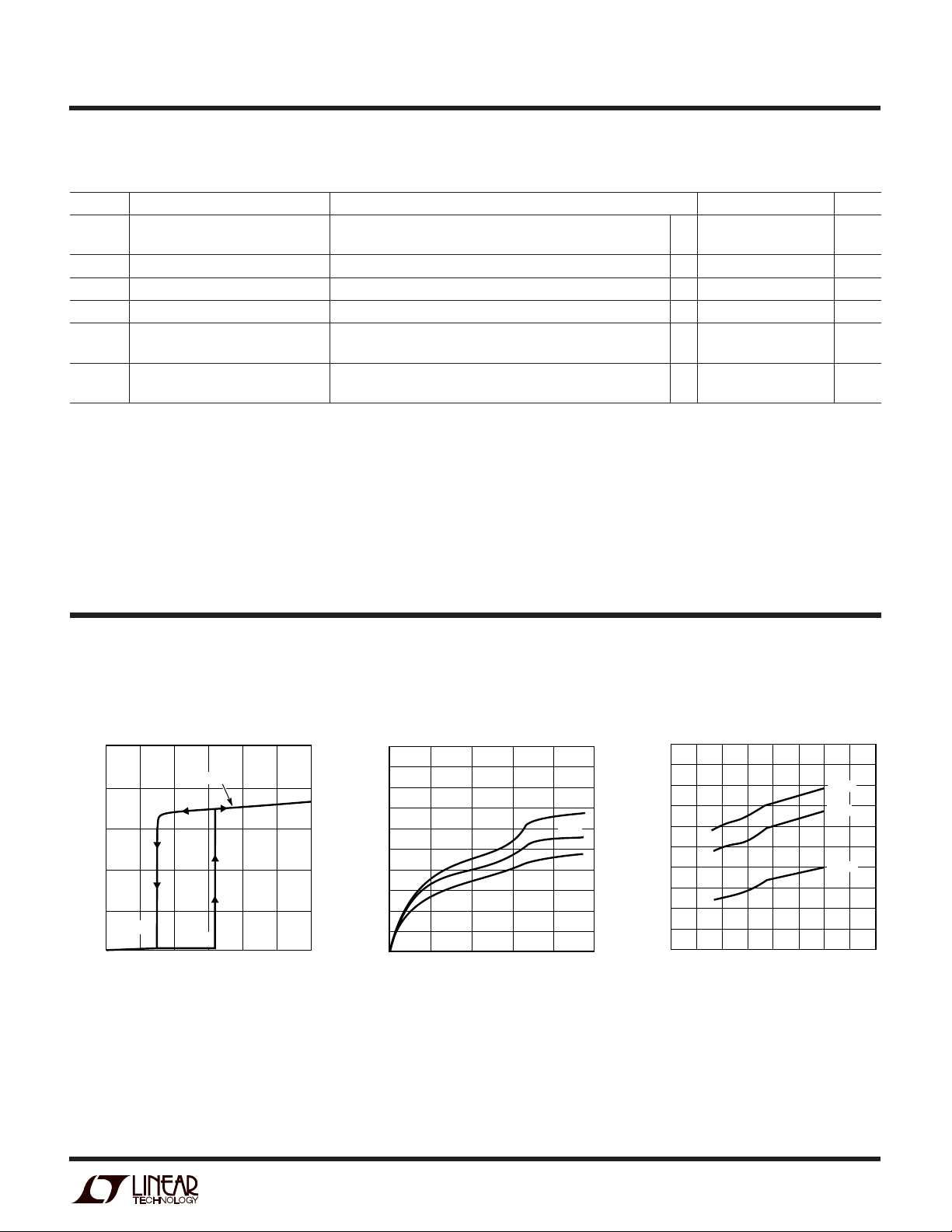
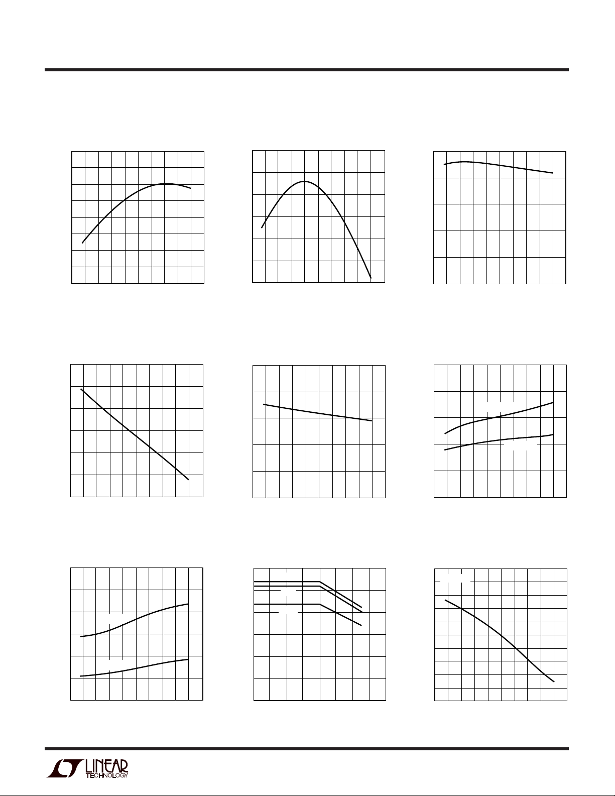
TYPICAL PERFORMANCE CHARACTERISTICS
Start-Up Supply Current vs
Supply Current vs Input Voltage
25
20
15
10
SUPPLY CURRENT (mA)
5
I
SHUT
0
0
5
25°C
I
START
10 15 20
INPUT VOLTAGE (V)
25 30
LT1103 G01
Input Voltage
500
450
400
350
300
250
200
150
100
START-UP SUPPLY CURRENT (µA)
50
0
0
125°C
–55°C
3
6
INPUT VOLTAGE (V)
9
12
25°C
LT1103 G02
1.76 (1.536 – DC) above 35% duty cycle.
LIM =
= 0.225
LIM
Quiescent Supply Current vs
Input Voltage
22
21
20
19
18
17
16
15
14
QUIESCENT SUPPLY CURRENT (mA)
13
12
0
515
15
10
20
INPUT VOLTAGE (V)
125°C
25°C
–55°C
35
30
25
40
LT1103 G03
5
Page 6
LT1103/LT1105
W
U
TYPICAL PERFORMANCE CHARACTERISTICS
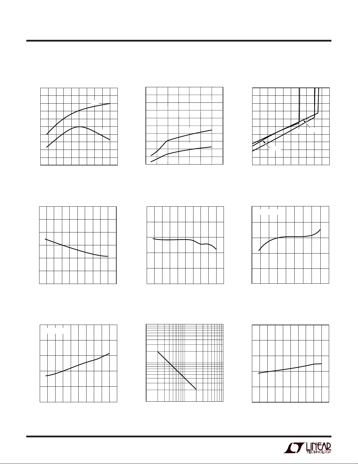
Quiescent Supply Current vs
Temperature
22
21
20
19
18
17
16
15
14
QUIESCENT SUPPLY CURRENT (mA)
13
12
–25
–50
–75
50 75 100 150
0
25
TEMPERATURE (°C)
VIN Start-Up Threshold vs
Temperature
17.5
17.0
16.5
16.0
15.5
START-UP THRESHOLD (V)
IN
V
15.0
30V
8V
125
LT1103 G04
175
Shutdown Supply Current vs
Input Voltage
500
450
A)
µ
400
350
300
250
200
150
100
SHUTDOWN SUPPLY CURRENT (
50
0
0
5
VC = 75mV
15
10
INPUT VOLTAGE (V)
VIN Shutdown Threshold vs
Temperature
8.0
7.7
7.4
7.1
SHUTDOWN THRESHOLD (V)
6.8
IN
V
VC = 0
20
Shutdown Supply Current vs
VC Voltage
500
450
400
350
300
250
200
150
SHUTDOWN CURRENT (µA)
100
50
30
LT1103 G05
35
25
0
0
–55°C
40
20
100 140 180
60
80
VC (mV)
25°C
120
125°C
160
200
LT1103 G06
Output Switch Frequency vs
Temperature
45
C
= 1000pF
OSC
43
41
39
37
OUTPUT SWITCH FREQUENCY (kHz)
14.5
–75
–50
0 50 100 150
–25 25 75 125
TEMPERATURE (°C)
Preset Switch Maximum Duty
Cycle vs Temperature
75
C
= 1000pF
OSC
72
69
66
63
PRESET SWITCH DUTY CYCLE (%)
60
–75
–25
25
0–50
TEMPERATURE (°C)
6
175
LT1103 G07
6.5
–75
–25
–50 0
75
25
50 100
TEMPERATURE (°C)
125
150
LT1103 G08
175
Switch Oscillator Frequency vs
Capacitance
1000
100
SWITCH FREQUENCY (kHz)
10
75
125
10050
150
LT1103 G10
175
100
1000 10000
CAPACITANCE (pF)
LT1103 G11
35
–50 0
–75
–25
TEMPERATURE (°C)
50 150
75
25
Overvoltage Lockout Threshold vs
Temperature
3.0
2.8
2.6
2.4
2.2
OVERVOLTAGE LOCKOUT THRESHOLD (V)
2.0
–75
–25
25
0–50
TEMPERATURE (°C)
75
10050
100
125
125
LT1103 G09
150
LT1103 G12
175
Page 7
W
TEMPERATURE (°C)
–75
5V LINE REGULATION (%/V)
0.03
0.04
0.05
125
LT1103 G18
0.02
0.01
0
–25
25
75
175
150
10050
0–50
TEMPERATURE (°C)
–75
15V GATE BIAS DROPOUT VOLTAGE (V)
1.5
2.0
2.5
125
LT1103 G21
1.0
0.5
0
–25
25
75
175
150
10050
0–50
TEMPERATURE (°C)
–75
SOFT-START RESET CURRENT (mA)
3
4
5
125
LT1103 G15
2
1
0
–25
25
75
175
150
10050
0–50
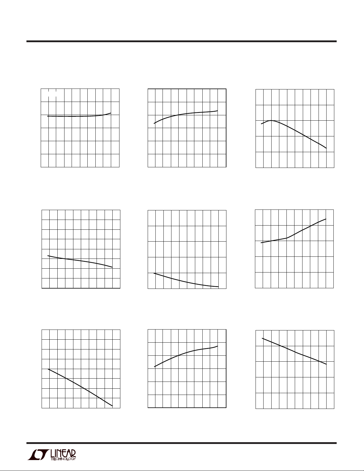
U
TYPICAL PERFORMANCE CHARACTERISTICS
LT1103/LT1105
OVLO Input Bias Current vs
Temperature
0
OVLO = 2V
–0.5
–1.0
–1.5
–2.0
–2.5
OVLO INPUT BIAS CURRENT (µA)
–3.0
–75
–50
0 50 100 150
–25 25 75 125
TEMPERATURE (°C)
5V Reference Voltage vs
Temperature
5.20
5.15
5.10
5.05
5.00
4.95
4.90
5V REFERENCE VOLTAGE (V)
4.85
LT1103 G13
175
Soft-Start Charging Current vs
Temperature
60
50
40
30
20
10
SOFT-START CHARGING CURRENT (µA)
0
–75
–50
0 50 100 150
–25 25 75 125
TEMPERATURE (°C)
5V Load Regulation vs
Temperature
0.025
0.020
0.015
0.010
0.005
5V LOAD REGULATION (%/mA)
Soft-Start Reset Current vs
Temperature
175
LT1103 G14
5V Line Regulation vs
Temperature
4.80
–75
–50
–25
0
TEMPERATURE (°C)
5V Reference Short-Circuit
Current vs Temperature
110
100
90
80
70
60
50
40
5V REFERENCE SHORT-CIRCUIT CURRENT (mA)
30
–25
–50
0
TEMPERATURE (°C)
–75
100
50
75
25
50
75
25
100
125
125
150
LT1103 G16
150
LT1103 G19
175
175
0
–25
–75
25
0–50
TEMPERATURE (°C)
15V Gate Bias Reference vs
Temperature
16.2
15.8
15.4
15.0
14.6
15V GATE BIAS REFERENCE (V)
14.2
13.8
–75
–50
0 50 100 150
–25 25 75 125
TEMPERATURE (°C)
75
125
10050
150
LT1103 G17
175
15V Gate Bias Dropout Voltage vs
Temperature
175
LT1103 G20
7
Page 8
LT1103/LT1105
W
U
TYPICAL PERFORMANCE CHARACTERISTICS
15V Gate Bias Short-Circuit
Current vs Temperature
130
110
90
70
50
30
15V GATE BIAS SHORT-CIRCUIT CURRENT (mA)
–75
–25
25
0–50
TEMPERATURE (°C)
75
125
10050
Feedback Threshold vs
Temperature
4.60
4.56
4.52
150
LT1103 G22
175
Low Switch Drive Lockout
Threshold vs Temperature
10.5
10.2
9.9
9.6
9.3
LOW SWITCH DRIVE LOCKOUT THRESHOLD (V)
9.0
–75
–25
25
0–50
TEMPERATURE (°C)
75
10050
125
FB Input Bias Current vs
Temperature (VC = 1V)
20
16
12
150
LT1103 G23
175
High Switch Drive Lockout
Threshold vs Temperature
20.0
19.5
19.0
18.5
18.0
17.5
HIGH SWITCH DRIVE LOCKOUT THRESHOLD (V)
17.0
–75
–50
0 50 100 150
–25 25 75 125
TEMPERATURE (°C)
Change in FB Input Bias Current
with Change in VC vs Temperature
(VC = 1V to 4V)
14
13
12
(µA/V)
C
11
175
LT1103 G24
4.48
FEEDBACK THRESHOLD (V)
4.44
4.40
–75
–25
25
0–50
TEMPERATURE (°C)
75
Error Amplifier Transconductance
vs Temperature
25000
20000
15000
10000
5000
ERROR AMPLIFIER TRANSCONDUCTANCE (µmho)
–75
–50 0
–25
50
75
25
TEMPERATURE (°C)
10050
100
125
125
150
LT1103 G25
150
LT1103 G28
8
4
FB INPUT BIAS CURRENT (µA)
0
–25
175
–75
25
0–50
TEMPERATURE (°C)
Error Amplifier Transconductance
and Phase vs Frequency
0.020
0.018
0.016
0.014
0.012
0.010
0.008
0.006
0.004
0.002
0
ERROR AMPLIFIER TRANSCONDUCTANCE (mho)
175
0.1 10 100 1000
PHASE
gm
1
FREQUENCY (kHz)
75
PHASE
10
9
WITH CHANGE IN V
8
CHANGE IN FB INPUT BIAS CURRENT
7
10050
125
175
150
LT1103 G26
–75
–50
0
25
–25
TEMPERATURE (°C)
75 125
50
100
150
LT1103 G27
175
Error Amplifier Voltage Gain vs
Temperature
gm
LT1103 G29
200
180
160
140
120
100
80
60
40
20
0
2500
2000
1500
PHASE (DEGREES)
1000
ERROR AMPLIFIER VOLTAGE GAIN (V/V)
500
–75
–50
–25
0
25
TEMPERATURE (°C)
100
50
75
125
150
LT1103 G30
175
8
Page 9
LPER
F
O
Error Amplifier Source Current vs
Temperature
350
325
300
275
250
225
200
175
ERROR AMPLIFIER SOURCE CURRENT (µA)
150
–50 0
–75
–25
50
75
25
TEMPERATURE (°C)
Error Amplifier Low Clamp
Voltage vs Temperature
(FB = 4.75V)
0.9
R
100
125
ATYPICA
150
LT1103 G31
175
UW
CCHARA TERIST
E
C
Error Amplifier Sink Current vs
Temperature
4.5
4.0
3.5
3.0
2.5
2.0
ERROR AMPLIFIER SINK CURRENT (mA)
1.5
1.5
–25 25 75 125
–50
–75
VC Switching Threshold Voltage
vs Temperature
ICS
0 50 100 150
TEMPERATURE (°C)
LT1103 G32
175
LT1103/LT1105
Error Amplifier High Clamp
Voltage vs Temperature
(FB = 4V)
4.5
4.4
4.3
4.2
4.1
ERROR AMPLIFIER HIGH CLAMP VOLTAGE (V)
4.0
200
–75
–25
0–50
TEMPERATURE (°C)
75
125
25
10050
LT1103 Output Switch Leakage
Current vs Temperature
150
LT1103 G33
175
0.8
0.7
0.6
0.5
0.4
ERROR AMPLIFIER LOW CLAMP VOLTAGE (V)
0.3
–75
–50
0 50 100 150
–25 25 75 125
TEMPERATURE (°C)
LT1103 Switch Saturation Voltage
vs Temperature
1.2
1.0
0.8
0.6
0.4
0.2
LT1103 SWITCH SATURATION VOLTAGE (V)
0
–75
ISW = 1.5A
ISW = 0.5A
0 50 100 150
–25 25 75 125
–50
TEMPERATURE (°C)
LT1103 G34
LT1103 G38
175
175
1.3
1.1
0.9
SWITCHING THRESHOLD (V)
C
0.7
V
0.5
–75
–25
25
0–50
TEMPERATURE (°C)
LT1103 VSW Current Limit vs
Duty Cycle
3.0
2.5
2.0
1.5
CURRENT LIMIT (A)
SW
1.0
0.5
LT1103 V
0
0
–55°C
125°C
10
25°C
30 50 70
20 40
DUTY CYCLE (%)
160
VSW = 45V
120
80
40
0
75
10050
125
175
150
LT1103 G35
LT1103 OUTPUT SWITCH LEAKAGE CURRENT (µA)
–75
–25
0–50
TEMPERATURE (°C)
VSW = 15V
75
125
25
10050
150
LT1103 G36
175
LT1103 VSW Current Limit vs
Temperature
3.0
DC = 25%
2.9
2.8
2.7
2.6
2.5
CURRENT LIMIT (A)
2.4
SW
2.3
2.2
LT1103 V
2.1
60
80
LT1103 G39
2.0
–75
–50
–25
0
25
TEMPERATURE (°C)
50 100 150
75
125
LT1103 G40
175
9
Page 10
LT1103/LT1105
TEMPERATURE (°C)
–75
LT1105 V
SW
FALL TIME (ns)
60
80
100
125
LT1103 G45
40
20
0
–25
25
75
175
150
10050
0–50
C
LOAD
= 4700pF
C
LOAD
= 1000pF
LPER
F
O
R
ATYPICA
UW
CCHARA TERIST
E
C
ICS
LT1103 Driver Current vs
Temperature
50
40
30
20
10
LT1103 DRIVER CURRENT (mA/A)
0
–75
–25
0–50
TEMPERATURE (°C)
75
25
LT1105 Current Limit Threshold
Voltage vs Temperature
450
DC = 25°C
425
400
375
350
325
LT1105 VSW Low Saturation
Voltage vs Temperature
3.0
2.5
2.0
1.5
1.0
LOW SATURATION VOLTAGE (V)
SW
0.5
LT1105 V
0
–75
10050
125
175
150
LT1103 G41
–50
0 50 100 150
–25 25 75 125
TEMPERATURE (°C)
ISW = 750mA
ISW = 200mA
175
LT1103 G42
LT1105 VSW Rise Time vs
Temperature
100
80
C
= 4700pF
C
LOAD
LOAD
= 1000pF
60
RISE TIME (ns)
SW
40
LT1105 V
20
LT1105 VSW High Saturation
Voltage vs Temperature
3.0
2.5
2.0
1.5
1.0
HIGH SATURATION VOLTAGE (V)
SW
0.5
LT1105 V
0
–75
–50
ISW = 750mA
ISW = 200mA
0 50 100 150
–25 25 75 125
TEMPERATURE (°C)
LT1105 VSW Fall Time vs
Temperature
175
LT1103 G43
300
LT1105 CURRENT LIMIT THRESHOLD VOLTAGE (mV)
–75
–50
10
0 50 100 150
–25 25 75 125
TEMPERATURE (°C)
LT1103 G46
175
0
–75
–25
25
0–50
TEMPERATURE (°C)
75
10050
125
175
150
LT1103 G44
Page 11

UUU
PIN FUNCTIONS
LT1103/LT1105
LT1103
FB: The Feedback pin is the inverting input to the sampling
error amplifier. The noninverting input is tied to a 4.5V
reference. The FB pin is used for output voltage sensing.
The input bias current is a function of the control pin V
voltage and can be used for load regulation compensation
by including a resistor in series with the FB pin. The
sampling error amplifier has a typical gm of 0.012 mhos
and the output of the sampling error amplifier has asymmetrical slew rate to reduce overshoot during start-up
conditions or following the release of an output overload.
VC: The VC control pin is used for frequency compensa-
tion, current limiting and shutdown. It is the high impedance output of the sampling error amplifier and the input
of the current limit comparator.
GND: The Ground pin acts as both the negative sense
point for the internal sampling error amplifier feedback
signal and as the high current path for the 2A switch.
Also, the case of the 7-lead TO-220 is connected to
ground. Proper connections to ground for signal paths
and high current paths must be made in order to insure
good load regulation.
OSC: The Oscillator pin sets the operating frequency of the
regulator with one external capacitor to ground. Maximum
duty cycle can also be adjusted by using an external
resistor to alter the charge/discharge ratio.
VIN: The Input Supply pin is designed to operate with
voltages of 12V to 30V. The supply current is typically
200µA up to the start-up threshold of 16V. Normal operating supply current is fairly flat at 18mA down to the
shutdown threshold of 7V. Switching is inhibited for V
less than 12V due to the gate drive detection circuit.
15V: A 15V reference is used to bias the gate of an external
power FET. The voltage temperature coefficient is typically
3mV/°C and the output can source 30mA. Typical dropout
voltage is 1.5V for VIN less than 17V and 30mA of load
current.
C
IN
VSW: The Switch Output pin is the collector of the internal
NPN power switch. This pin has a typical ON resistance of
0.4Ω and a minimum breakdown voltage of 50V. This pin
also ties to the FET gate drive detection circuit.
LT1105
All functions on the LT1105 are equivalent to the LT1103
with the exception of the VSW pin and the I
availability of the OVLO, 5V, and SS functions.
OVLO: The Overvoltage Lockout pin inhibits switching
when the pin is pulled above its threshold voltage of 2.5V.
OVLO is implemented with a resistor divider network from
the rectified DC line and is used to protect the external FET
from an overvoltage condition in the off state. This function is only available on the 14-lead PDIP.
5V: A 5V reference is available to power primary-side
circuitry. The temperature coefficient is typically
50ppm/°C and the output can source 25mA. This function is only available on the 14-lead PDIP.
SS: The Soft-Start pin is used to either program start-up
time with a capacitor to ground or to set external current
limit with a resistor divider. The SS pin has a 40µA pull-up
current and is reset to 0V by a 1mA pull-down current
during start-up and shutdown. This function is only available on the 14-lead PDIP.
VSW: The Switch Output pin is the output of a 1A NPN
totem-pole stage. The VSW pin turns the external FET on by
pulling its gate high. Break-Before-Make action of 200ns
on each switch edge is built in to eliminate cross conduction currents.
I
: The I
LIM
and requires the use of a noninductive, power sense
resistor from I
current limit threshold voltage is 350mV. The typical input
bias current is 100µA out of the pin.
pin is the input to the current limit amplifier
LIM
to ground to set current limit. The typical
LIM
pin and the
LIM
11
Page 12

LT1103/LT1105
W
BLOCK DIAGRA S
15V
15V
GATE
BIAS
OSC
LT1103
GATE
BIAS
DETECT
V
SW
V
0VLO
START-UP
16V
IN
7V
2.5V
5V
V
REF
5V
FB
OSCILLATOR
4.5V
OVERVOLTAGE
LOCKOUT
+
–
SAMPLING
ERROR AMP
= 0.012
g
m
LOGIC
COMP
0.15V
SHUT
DOWN
SPIKE
BLANK
DRIVER
ANTISAT
CURRENT
LIMIT
AMP
AV = 10
+
0.15Ω
–
6V
40µA
RESET
LT1103 BD
V
C
SS
GND
12
Page 13

W
BLOCK DIAGRA S
15V
15V
GATE
BIAS
OSC
LT1105
GATE
BIAS
DETECT
LT1103/LT1105
V
0VLO
START-UP
16V
IN
5V
FB
7V
5V
V
REF
2.5V
OSCILLATOR
4.5V
OVERVOLTAGE
LOCKOUT
+
–
SAMPLING
ERROR AMP
g
= 0.012
m
LOGIC
COMP
0.15V
SHUT
DOWN
SPIKE
BLANK
V
DRIVER
V
SW
DRIVER
ANTISAT
CURRENT
LIMIT
AMP
AV = 10
+
I
LIM
–
6V
40µA
RESET
LT1105 BD
C
SS
GND
13
Page 14

LT1103/LT1105
U
ATIOOPER
LT1103
The LT1103 is a current mode switcher. Switch duty cycle
is controlled by switch current rather than directly by the
output voltage. Referring to the block diagram, the switch
is turned on at the start of each oscillator cycle. It is turned
off when switch current reaches a predetermined level.
Control of output voltage is obtained by using the output
of a voltage sensing error amplifier to set current trip level.
This technique has several advantages. First, it has immediate response to input voltage variations, unlike ordinary
switchers which have notoriously poor line transient
response. Second, it reduces the 90° phase shift at mid
frequencies in the transformer. This greatly simplifies
closed-loop frequency compensation under widely varying input voltage or output load conditions. Finally, it
allows simple pulse-by-pulse current limiting to provide
maximum switch protection under output overload or
short-circuit conditions.
A start-up loop with hysteresis allows the IC supply
voltage to be bootstrapped from an extra primary side
winding on the power transformer. From 0V to 16V on VIN,
the LT1103 is in a prestart mode and total input current is
typically 200µA. Above 16V, up to 30V, the 6V regulator
that biases the internal circuitry and the externally available 15V regulator is turned on. The internal circuitry
remains biased on until VIN drops below 7V and the part
returns to the prestart mode. Output switching stops when
the VSW drive is less than 10V corresponding to VIN of
about 12V.
The oscillator provides the basic clock for all internal
timing. Frequency is adjustable to 200kHz with one external capacitor from OSC to ground. The oscillator turns on
the output switch via the logic and driver circuitry. Adaptive antisat circuitry detects the onset of saturation in the
power switch and adjusts driver current instantaneously
to limit switch saturation. This minimizes driver dissipation and provides very rapid turn-off of the switch.
The LT1103 is designed to drive the source of an external
power FET in common gate configuration. The 15V regulator biases the gate to guarantee the FET is on when the
switch is on. Special drive detection circuitry senses the
gate bias voltage and prevents the output switch from
turning on if the gate voltage is less than 10V or greater
than 20V, the industry standards for power MOSFET
operation.
The switch current is sensed internally and amplified to
trip the comparator and turn off the switch according to
the VC pin control voltage. A blanking circuit suppresses
the output of the current limit comparator for 500ns at the
beginning of each switch cycle. This prevents false tripping of the comparator due to current spikes caused by
external parasitic capacitance and diode stored charge.
The 4.5V Zener-based reference biases the positive input
of the sampling error amplifier. The negative input (FB) is
used for output voltage sensing. The sampling error
amplifier allows the LT1103 to operate in fully isolated
flyback mode by regulating from the flyback voltage of the
bootstrap winding. The leakage inductance spike at the
leading edge of the flyback waveform is ignored with a
blanking circuit. The flyback waveform is directly proportional to the output voltage in a transformer-coupled
flyback topology. Output voltages are fully floating up to
the breakdown voltage of the transformer windings. Multiple floating outputs are easily obtained with additional
windings.
The error signal developed at the comparator input is
brought out externally. This VC pin has three functions
including frequency compensation, current limit adjustment and total regulator shutdown. During normal operation, this pin sits at a voltage between 1.2V (low output
current) and 4.4V (high output current). The error amplifier is a current output (gm) type, so this voltage can be
externally clamped for adjusting current limit. Switch duty
cycle goes to zero if the VC pin is pulled to ground through
a diode, placing the LT1103 in an idle mode. Pulling the V
pin below 0.15V causes total regulator shutdown and
places the LT1103 in a prestart mode.
LT1105
The LT1105 is a current mode switcher. Switch duty cycle
is controlled by switch current rather than directly by
output voltage. Referring to the block diagram, the switch
is turned on at the start of each oscillator cycle. It is turned
off when switch current reaches a predetermined level.
C
14
Page 15

LT1103/LT1105
U
ATIOOPER
Control of output voltage is obtained by using the output
of a voltage sensing error amplifier to set current trip level.
This technique has several advantages. First, it has immediate response to input voltage variations, unlike ordinary
switchers which have notoriously poor line transient response. Second, it reduces the 90° phase shift at
midfrequencies in the transformer. This greatly simplifies
closed-loop frequency compensation under widely varying input voltage or output load conditions. Finally, it
allows simple pulse-by-pulse current limiting to provide
maximum switch protection under output overload or
short-circuit conditions.
A start-up loop with hysteresis allows the IC supply
voltage to be bootstrapped from an extra primary side
winding on the power transformer. From 0V to 16V on VIN,
the LT1105 is in prestart mode and total input current is
typically 200µA. Above 16V, up to 30V, the 6V regulator
that biases the internal circuitry and the externally available 5V and 15V regulators are turned on. The internal
circuitry remains biased on until VIN drops below 7V and
the part returns to prestart mode. Output switching stops
when the 15V gate bias reference is less than 10V corresponding to VIN of about 12V.
The oscillator provides the basic clock for all internal
timing. Frequency is adjustable to 200kHz with one external capacitor from OSC to ground. The oscillator turns on
the output switch via the logic and driver circuitry.
The LT1105 is designed to drive the gate of an external
power FET in common source configuration. The drivers
and the 1A maximum totem-pole output stage are biased
from the 15V gate bias reference. Special drive detection
circuity senses the gate bias reference voltage and prevents the output switch from turning on if this voltage is
less than 10V or greater than 20V. Break-Before-Make
action of 200ns is built into each switch edge to eliminate
cross conduction currents.
suppresses the output of the current limit comparator for
500ns at the beginning of each switch cycle. This prevents
false tripping of the comparator due to current spikes
caused by external parasitic capacitance and diode stored
charge.
A 4.5V Zener-based reference biases the positive input of
the sampling error amplifier. The negative input (FB) is
used for output voltage sensing. The sampling error
amplifier allows the LT1105 to operate in fully isolated
flyback mode by regulating the flyback voltage of the
bootstrap winding. The leakage inductance spike at the
leading edge of the flyback waveform is ignored with a
blanking circuit. The flyback waveform is directly proportional to the output voltage in the transformer coupled
flyback topology. Output voltages are fully floating up to
the breakdown voltage of the transformer windings. Multiple floating outputs are easily obtained with additional
windings.
The error signal developed at the comparator input is
brought out externally. The VC pin has three functions
including frequency compensation, current limit adjustment and total regulator shutdown. During normal operation, this pin sits at a voltage between 1.2V (low output
current) and 4.4V (high output current). The error amplifier is a current output (gm) type, so this voltage can be
externally clamped for adjusting current limit. Switch duty
cycle goes to zero if the VC pin is pulled to ground through
a diode, placing the LT1105 in an idle mode. Pulling the V
pin below 0.15V causes total regulator shutdown and
places the LT1105 in prestart mode.
The SS pin implements soft-start with one external capacitor to ground. The internal pull-up current and clamp
transistor limit the voltage at VC to one diode drop above
the voltage at the SS pin, thereby controlling the rate of rise
of switch current in the regulator. The SS pin is reset to 0V
when the LT1105 is in prestart mode.
C
Switch current is sensed externally through a precision,
power resistor. This allows for greater flexibility in switch
current and output power than allowed by the LT1103. The
voltage across the sense resistor is fed into the I
amplified to trip the comparator and turn off the switch
according to the VC pin control voltage. A blanking circuit
LIM
pin and
A final protection feature includes overvoltage lockout
monitoring of the main supply voltage on the OVLO pin. If
the OVLO pin is greater than 2.5V, the output switch is
prevented from turning on. This function can be disabled
by grounding the OVLO pin.
15
Page 16

LT1103/LT1105
U
WUU
APPLICATIONS INFORMATION
Bootstrap Start
It is inefficient as well as impractical to power a switching
regulator control IC from the rectified DC input as this
voltage is several hundred volts. Self-biased switching
regulator topologies take advantage of a lower voltage
auxiliary winding on the power transformer or inductor to
power the regulator, but require a start-up cycle to begin
regulation.
Start-up circuitry with hysteresis built into the LT1103/
LT1105 allows the input voltage to increase from 0V to
16V before the regulator tries to start. During this time the
start-up current of the switching regulator is typically
200µA and all internal voltage regulators are off. The low
quiescent current allows the input voltage to be trickled up
with only 500µA of current from the rectified DC line
voltage, thereby minimizing power dissipation in the startup resistor. At 16V, the internal voltage regulators are
turned on and switching begins. If enough power feeds
back through the auxiliary winding to keep the input
voltage to the switching regulator above 12V, then switching
continues and a bootstrap start is accomplished. If the
input voltage drops below 12V, then the FET drive detection
circuit locks out switching. The input voltage continues to
fall as the VIN bypass capacitor is discharged by the
normal quiescent current of the LT1103/LT1105. Once the
input voltage falls below 7V, the internal voltage regulators
are turned off and the switching regulator returns to the
low start-up current state. A continuous “burp start” mode
indicates a fault condition or an incomplete power loop.
The trickle current required to bootstrap the regulator
input voltage is typically generated with a resistor from the
rectified DC input voltage. When combined with the
regulator input bypass capacitor, the start-up resistor
creates a ramp whose slope governs the turn-on time of
the regulator as well as the period of the “burp start” mode.
The design trade-offs are power dissipated in the trickle
resistor, the turn-on time of the regulator, and the hold-up
time of the regulator input bypass capacitor. The value of
the start-up resistor is set by the minimum rectified DC
input voltage to guarantee sufficient start-up current. The
recommended minimum trickle current is 500µA. The
power rating of the start-up resistor is set by the maximum
rectified DC input voltage. A final consideration for the
start-up resistor is to insure that the maximum voltage
rating of the resistor is not exceeded. Typical carbon film
resistors have a voltage rating of 250V. The most reliable
and economical solution for the start-up resistor is generally
provided by placing several 0.25W resistors in series.
The LT1103/LT1105 is designed to operate with supply
pin voltages up to 30V. However, the auxiliary bias winding
should be designed for a typical output voltage of 17V to
minimize IC power dissipation and efficiency loss.
Allowances must also be made for cross regulation of the
bias voltage due to variations in the rectified DC line
voltage and output load current.
Soft-Start
Soft-start refers to the controlled increase of switch
current from a start-up or shutdown state. This allows the
power supply to come up to voltage in a controlled
manner and charge the output capacitor without activating
current limit. In general, soft-start is not required on the
LT1105 due to the design of the sampling error amplifier
gm stage which generates asymmetrical slew capability
on the VC pin.
This feature exhibits itself as a typical 3mA sink current
capability on the VC pin whereas source current is only
275µA. The low gm of the error amplifier allows smallvalued compensation capacitors to be used on VC. This
allows the sink current to slew the compensation capacitor
quickly. Therefore, overshoot of the output voltage on
start-up sequences and recovery from overload or shortcircuit conditions is prevented. However, if a longer startup period is required, the soft-start function can be used.
Soft-start is implemented with an internal 40µA pull-up
and a transistor clamp on the VC pin so that a single
external capacitor from SS ground can define the linear
ramp function. The voltage at VC is limited to one V
above the soft-start pin (SS). The time to maximum switch
current is defined as the capacitance on SS multiplied by
the active range in volts of the VC pin divided by the pullup current:
C •(3.2V)
T
40 A=µ
BE
16
Page 17

LT1103/LT1105
U
WUU
APPLICATIONS INFORMATION
SS is reset to 0V whenever VIN is less than 7V (prestart
mode) or when shutdown is activated by pulling VC below
0.15V. The SS pin has a guaranteed reset sink current of
1mA when either the regulator supply voltage VIN falls
below 7V or the regulator is placed in shutdown.
Shutdown
The LT1103/LT1105 can be put in a low quiescent current
shutdown mode by pulling VC below 150mV. In the
shutdown mode the internal voltage regulators are turned
off, SS is reset to 0V and the part draws less than 200µA.
To initiate shutdown, about 400µA must be pulled out of
VC until the internal voltage regulators turn off. Then, less
than 50µA pull-down current is required to maintain
shutdown. The shutdown function has about 60mV of
hysteresis on the VC pin before the part returns to normal
operation. Soft-start, if used, controls the recovery from
shutdown.
5V Reference
Ground (LT1103)
The ground pin of the LT1103 is important because it acts
as the negative sense point for the internal error amplifier
feedback signal, the negative sense point for the current
limit amplifier, and as the high current path for the 2A
switch. The tab of the 7-lead TO-220 is internally connected
to GND (Pin 4).
To avoid degradation of load regulation, the feedback
resistor divider string and the reference side of the bias
winding should be directly connected to the ground pin on
the package. These ground connections should not be
mixed with high current carrying ground return paths. The
length of the switch current ground path should be as
short as possible to the input supply bypass capacitor and
low resistance for best performance. The case of the
LT1103 package is desirable to use as the high current
ground return path as this is a lower resistive and inductive
path than that of the actual package pin and will help
minimize voltage spikes associated with the high dI/dt
switch current.
A 5V reference output is available for the user’s convenience
to power primary-side circuitry or to generate a clamp
voltage for switch current limiting. The output will source
25mA and the voltage temperature coefficient is typically
50ppm/°C. If bypassing of the 5V reference is required, a
0.1µF is recommended. Values of capacitance greater
than 1µF may be susceptible to ringing due to decreased
phase margin. In such cases, the capacitive load can be
isolated from the reference output with a small series
resistor at the expense of load regulation performance.
Overvoltage Lockout
The switching supply and primarily the external power
MOSFET can be protected from an extreme surge of the
input line voltage with the overvoltage lockout feature
implemented on the OVLO pin. If the voltage on OVLO rises
above its typical threshold voltage of 2.5V, output switching
is inhibited. This feature can be implemented with a
resistive divider off of the rectified DC input voltage. This
feature is only available on the LT1105 in the 14-lead PDIP
and must be tied to ground if left unused.
Avoiding long wire runs to the ground pin minimizes load
regulation effects and inductive voltages created by the
high dI/dt switch current. Ground plane techniques should
also be used and will help keep EMI to a minimum.
Grounding techniques are illustrated in the Typical
Applications section.
Ground (LT1105)
The ground pin of the LT1105 is important because it acts
as the negative sense point for the internal error amplifier
feedback signal and as the negative sense point for the
current limit amplifier. The LT1105 8-pin PDIP has Pin 1
as its ground. The LT1105 14-pin PDIP has Pin 1 and
Pin 7 as grounds and must be tied together for proper
operation.
To avoid degradation of load regulation, the feedback
resistor divider should be directly connected to the package
ground pin. These ground connections should not be
mixed with high current carrying ground return paths. The
length of the switch current ground path should be as
short as possible to the input supply bypass capacitor and
17
Page 18

LT1103/LT1105
U
WUU
APPLICATIONS INFORMATION
low resistance for best performance. This will help minimize
voltage spikes associated with the high dI/dt switch current.
Avoiding long wire runs to the ground pin minimizes load
regulation effects and inductive voltages created by the
high dI/dt switch current. Ground plane techniques should
also be used and will help keep EMI to a minimum.
Grounding techniques are illustrated in the Typical
Applications section.
Oscillator
The oscillator of the LT1103/LT1105 is a linear ramp type
powered from the internal 6V bias line. The charging
currents and voltage thresholds are generated internally
so that only one external capacitor is required to set the
frequency. The 150µA pull-up current, which is on all the
time, sets the preset maximum on-time of the switch and
the 450µA pull-down current which is turned on and off,
sets the dead time. The threshold voltages are typically 2V
and 4.5V, so for a 400pF capacitor the ramp-up time of the
voltage on the OSC pin is 6.67µs and the ramp-down time
is 3.3µs, resulting in an operating frequency of 100kHz.
Although the oscillator, as well as the rest of the switching
regulator, will function at higher frequencies, 200kHz is
the practical upper limit that will allow control range for
line and load regulation. The lowest operating frequency is
limited by the sampling error amplifier to about 10kHz.
The frequency temperature coefficient is typically – 80ppm/
°C with a good low T.C. capacitor. This means that with a
low temperature coefficient capacitor, the temperature
coefficient of the currents and the temperature coefficient
of the thresholds sum to –80ppm/°C over the commercial
temperature range. Bowing in the temperature coefficient
of the currents affects the frequency about ±3% at the
extremes of the military temperature range. The capacitor
type chosen will have a direct effect on the frequency
tempco.
Maximum duty cycle is set internally by the pull-up and
pull-down currents, independent of frequency. It can be
adjusted externally by modifying the fixed pull-up current
with an additional resistor. In practice, one resistor from
the OSC pin to the 5V reference or to ground does the job.
Note that the capacitor value must change to maintain the
same frequency. For example, a 24k resistor from 5V to
OSC and a 440pF capacitor from OSC to ground will yield
100kHz with 50% maximum duty cycle. A 56k resistor and
a 280pF capacitor from OSC to ground will yield 100 kHz
with 80% maximum duty cycle.
The oscillator can be synchronized to an external clock by
coupling a sync pulse into the OSC pin. The width of this
pulse should be a minimum of 500ns. The oscillator can
only be synchronized up in frequency and the synchronizing
frequency must be greater than the maximum possible
unsynchronized frequency (for the chosen oscillator
capacitor value). The amplitude of the sync pulse must be
chosen so that the sum of the oscillator voltage amplitude
plus the sync pulse amplitude does not exceed the 6V bias
reference. Otherwise, the oscillator pull-up current source
will saturate and erroneous operation will result. If the
LT1103/LT1105 is positioned on the primary side of the
transformer and the external clock on the isolated secondary
output side, the sync signal must be coupled into the OSC
pin using a pulse transformer. The pulse transformer must
meet all safety/isolation requirements as it also crosses
the isolation boundary. An example of externally
synchronizing the oscillator is shown in the Typical
Applications section.
Gate Biasing (LT1103)
The LT1103 is designed to drive an external power MOSFET
in the common gate or cascode connection with the V
pin. The advantage is that the switch current can be sensed
internally, eliminating a low value, power sense resistor.
The gate needs to be biased at a voltage high enough to
guarantee that the FET is saturated when the open-collector
source drive is on. This means 10V as specified in FET data
sheets, plus 1V for the typical switch saturation voltage,
plus a couple of volts for temperature variations and
processing tolerances. This leads to 15V for a practical
gate bias voltage.
Power MOSFETs are well suited to switching power supplies
because their high speed switching characteristics promote
high switching efficiency. To achieve high switching speed,
SW
18
Page 19

LT1103/LT1105
U
WUU
APPLICATIONS INFORMATION
A special circuit in the LT1103 senses the voltage at V
prior to turning on the switch. VSW is tied to the source of
the FET and should represent the bias voltage on the gate
when the switch is off. When the switch first turns off, the
drain flies back until it is clamped by a snubber network.
The source also flies high due to parasitic capacitive
coupling on the FET and parasitic inductance of the leads.
An extra diode from the source to the gate or VIN will
provide insurance against fault conditions that might
otherwise damage the FET. The diode clamps the source
to one diode drop above the gate or VIN, thereby limiting
the gate source reverse bias. Once the energy in the
leakage inductance spike is dissipated and the primary is
being regulated to its flyback voltage, the diode shuts off.
The source is then floating and its voltage will be close to
the gate voltage. If the sensed voltage on VSW is less than
10V or greater than 20V, the circuit prevents the switch
from turning on. This protects the FET from dissipating
high power in a nonsaturated state or from excessive gatesource voltage. The oscillator continues to run and the net
effect is to skip switching cycles until the gate bias voltage
is corrected. One consequence of the gate bias detection
circuit is that the start-up window is 6V if the gate is biased
from VIN and to 4V if the gate is biased from the 15V
output. This influences the size of the bypass capacitor on
VIN.
SW
keep the switch just at the edge of saturation. Very low
switch current results in nearly zero driver current and
high switch currents automatically increase driver current
as necessary. The ratio of switch current to driver current
is approximately 30:1. This ratio is determined by the
sizing of the extra emitter and the value of the current
source feeding the driver circuitry. The quasisaturation
state of the switch permits rapid turn-off without the need
for reverse base emitter voltage drive.
Gate Biasing (LT1105)
The LT1105 is designed to drive an external power MOSFET
in the common source configuration with the totem-pole
output VSW pin. The advantage is added switch current
flexibility (limited only by the choice of external power
FET) and higher output power applications than allowed by
LT1103. An external, noninductive, power sense resistor
must be used in series with the source of the FET to detect
switch current and must be tied to the input of the current
limit amplifier. The gate needs to be biased at a voltage
high enough to guarantee that the FET is saturated when
the totem-pole gate drive is on. This means 10V as
specified in FET data sheets, plus the totem-pole high side
saturation voltage plus a couple of volts for temperature
variations and processing tolerances. This leads to 15V for
a practical gate bias voltage.
VSW Output (LT1103)
The VSW pin of the LT1103 is the collector of an internal
NPN power switch. This NPN has a typical on resistance of
0.4Ω and a typical breakdown voltage (BV
switching times and high efficiency are obtained by using
a special driver loop which automatically adapts base drive
current to the minimum required to keep the switch in a
quasisaturated state. The key element in the loop is an
extra emitter on the output power transistor as seen in the
block diagram. This emitter carries no current when the
NPN output transistor collector is high (unsaturated). In
this condition, the driver circuit can deliver very high base
drive to the switch for fast turn-on. When the switch
saturates, the extra emitter acts as a collector of an NPN
operating in inverted mode and pulls base current away
from the driver. This linear feedback loop serves itself to
) of 75V. Fast
CBO
Power MOSFETs are well suited to switching power supplies
because their high speed switching characteristics promote
high switching efficiency. To achieve high switching speed,
the gate capacitance must be charged and discharged
quickly with high peak currents. In particular, the turn-off
current can be as high as the peak switch current. The
switching speed is controlled by the impedance seen by
the gate capacitance. Practically speaking, zero impedance
is not desirable because of the high frequency noise spikes
introduced to the system. The gate bias supply which
drives the totem-pole output stage should be bypassed
with a 1µF low ESR capacitor to ground. This capacitor
supplies the energy to charge the gate capacitance during
gate drive turn-on. The power MOSFET should have a 5Ω
resistor or larger in series with its gate from the VSW pin
to define the source impedance.
19
Page 20

LT1103/LT1105
U
WUU
APPLICATIONS INFORMATION
The LT1105 provides a 15V regulated output intended for
driving the totem-pole output stage. It will source 30mA
into a capacitive load with no stability problems. The
output voltage temperature coefficient is 3mV/°C. If V
drops below 17V, the 15V output follows about 2.0V below
VIN until the part shuts down. If the 15V output is pulled
above 17.5V, it will sink 5mA.
A special circuit in the LT1105 senses the voltage at the
15V regulated output prior to turning on the switch. The
15V regulator drives the totem-pole output stage and the
VSW pin will pull the gate of the FET very close to the value
of the 15V output when VSW turns on. Therefore, the 15V
output represents what the gate bias voltage on the FET
will be when the FET is turned on. If the sensed voltage on
the 15V output is less than 10V or greater than 20V, the
circuit prevents the switch from turning on. This protects
the FET from dissipating high power in a nonsaturated
state or from excessive gate-source voltage. The oscillator
continues to run and the net effect is to skip switching
cycles until the gate bias voltage is corrected. One
consequence of the gate bias detection circuit is that the
start-up window is 4V. This influences the size of the
bypass capacitor on VIN.
VSW Output (LT1105)
The VSW pin of the LT1105 is the output of a 1A totem-pole
driver stage. This output stage turns an external power
MOSFET on by pulling its gate high. Break-Before-Make
action of 200ns is built into each switch edge to eliminate
cross-conduction currents. Fast switching times and high
efficiency are obtained by using a low loss output stage
and a special driver loop which automatically adapts base
drive current to the totem-pole low side drive. The key
element in the loop is an extra emitter on the output pulldown transistor as seen in the block diagram. This emitter
carries no current when the low side transistor collector
is high (unsaturated). In this condition, the driver can
deliver very high base drive to the output transistor for fast
turn-off. When the low side transistor saturates, the extra
emitter acts as a collector of an NPN operating in inverted
mode and pulls base current away from the driver. This
linear feedback loop serves itself to keep the switch just at
IN
the edge of saturation. This results in nearly zero driver
current. The quasisaturation state of the low side switch
permits rapid turn-on of the external FET when VSW pulls
high.
Fully Isolated Flyback Mode
A unique sampling error amplifier included in the control
loop of the LT1103/LT1105 eliminates the need for an
optoisolator while providing ±1% line and load regulation
in a magnetic flux-sensed flyback converter. In this mode,
the flyback voltage on the primary during “switch off” time
is sensed and regulated. It is difficult to derive a feedback
signal directly from the primary flyback voltage as this
voltage is typically several hundred volts. A dedicated
winding is not required because the bias winding for the
regulator lends itself to flux-sensing. Flux-sensing made
practical simplifies the design of off line power supplies by
minimizing the total number of external components and
reduces the components which must cross the isolation
barrier to one, the transformer. This inherently implies
greater safety and reliability. The transformer must be
optimized for coupling between the bias winding and the
secondary output winding(s) while maintaining the required
isolation and minimizing the parasitic leakage inductances.
Although magnetic flux-sensing has been used in the past,
the technique has exhibited poor output voltage regulation
due to the parasitics present in a transformer coupled
design. Transformers which provide the safety and isolation
as required by various international safety/regulatory
agencies also provide the poorest output voltage regulation.
Solutions to these parasitic elements have been achieved
with the novel sampling error amplifier of the LT1103/
LT1105. A brief review of flyback converter operation and
the problems which create a poorly regulated output will
provide insight on how the sampling error amplifier of the
LT1103/LT1105 addresses the regulation issue of magnetic
flux sensed converters.
The following figure shows a simplified diagram of a
flyback converter using magnetic flux sensing. The major
parasitic elements present in the transformer coupled
design are indicated. The relationships between the primary
20
Page 21

LT1103/LT1105
U
WUU
APPLICATIONS INFORMATION
voltage, the secondary voltage, the bias voltage and the
winding currents are indicated in the figures found on the
following page for both continuous and discontinuous
modes of operation.
Simplified Flyback Converter
V
IN
L(Ik
)
V
PRI
S1
BIAS
L(lk
)
SEC
1:N
N = TURNS RATIO FROM SECONDARY TO PRIMARY.
N1 = TURNS RATIO FROM SECONDARY TO BIAS.
N2 = N/N1
L(lk
PRI
L(lk
SEC
R = PARASITIC WINDING, DIODE AND OUTPUT
1:N1
CAPACITOR RESISTANCE.
When the switch “turns on,” the primary winding sees the
input voltage and the secondary and bias windings go to
negative voltages as a function of the turns ratio. Current
builds in the primary winding as the transformer stores
energy. When the switch “turns off,” the voltage across
the switch flies back to a clamp level as defined by a
snubber network until the energy in the leakage inductance of the primary dissipates. Leakage inductance is one
of the main parasitic elements in a flux-sensed converter
and is modeled as an inductor in series with the primary
and secondary of the transformer. These parasitic inductances contribute to changes in the bias winding voltage
and thus the output voltage with increasing load current.
The energy stored in the transformer transfers through the
secondary and bias windings during “switch off” time.
Ideally, the voltage across the bias winding is set by the DC
output voltage, the forward voltage of the output diode,
and the turns ratio of the transformer after the energy in
the leakage inductance spike of the primary is dissipated.
This relationship holds until the energy in the transformer
drops to zero (discontinuous mode) or the switch turns on
again (continuous mode). Either case results in the voltage across the secondary and bias windings decreasing
D1
R
) = PRIMARY LEAKAGE INDUCTANCE.
) = SECONDARY LEAKAGE INDUCTANCE.
V
OUT
C1
COMMON
LT1103 AI01
to zero or changing polarity. Therefore, the voltage on the
bias winding is only valid as a representation of the output
voltage while the secondary is delivering current.
Although the bias winding flyback voltage is a representation of the output voltage, its voltage is not constant. For
a brief period following the leakage inductance spike, the
bias winding flyback voltage decreases due to nonlinearities
and parasitics present in the transformer. Following this
nonlinear behavior is a period where the bias winding
flyback voltage decreases linearly. This behavior is easily
explained. Current flow in the secondary decreases linearly at a rate determined by the voltage across the
secondary and the inductance of the secondary. The
parasitic secondary leakage inductance appears as an
impedance in series with the secondary winding. In addition, parasitic resistances exist in the secondary winding,
the output diode and the output capacitor. These impedances can be combined to form a lumped sum equivalent
and which cause a voltage drop as secondary current
flows. This voltage drop is coupled from the secondary to
the bias winding flyback voltage and becomes more significant as the output is loaded more heavily. This voltage
drop is largest at the beginning of “switch off” time and
smallest just prior to either all transformer energy being
depleted or the switch turning on again.
The best representation of the output voltage is just prior
to either all transformer energy being used up and the bias
winding voltage collapsing to zero or just prior to the
switch turning on again and the bias winding going
negative. This point in time also represents the smallest
forward voltage for the output diode. It is possible to
redefine the relationship between the secondary winding
voltage and the bias winding voltage as:
VVfI•R
V
BIAS
()
=
++
OUT P
N1
where Vf is the forward voltage of the output diode, I is the
current flowing in the secondary, RP is the lumped sum
equivalent secondary parasitic impedance and N1 is the
transformer turns ratio from the secondary to the bias
winding. It is apparent that even though the above point in
21
Page 22

LT1103/LT1105
U
WUU
APPLICATIONS INFORMATION
Flyback Waveform for Continuous Mode Operation
V
ZENER
PRIMARY SWITCH VOLTAGE
+ Vf + (I
[V
a
b
c
d
e
f
∆I
OUT
V
IN
AREA “a” = AREA “b” TO MAINTAIN
ZERO VOLTS ACROSS PRIMARY
0V
SECONDARY WINDING VOLTAGE
[V
+ Vf + (I
OUT
0V
AREA “c” = AREA “d” TO MAINTAIN
ZERO VOLTS ACROSS SECONDARY
N • V
IN
BIAS WINDING VOLTAGE
[V
+ Vf + (I
OUT
0V
AREA “e” = AREA “f” TO MAINTAIN
ZERO VOLTS ACROSS BIAS WINDING
N2 • V
IN
I
PRI
SEC
SEC
SEC
• RP)]/N
• RP)]
• RP)]/N1
Flyback Waveform for Discontinuous Mode Operation
V
ZENER
PRIMARY SWITCH VOLTAGE
+ Vf + (I
[V
a
b
c
d
e
f
OUT
V
IN
AREA “a” = AREA “b” TO MAINTAIN
ZERO VOLTS ACROSS PRIMARY
0V
SECONDARY WINDING VOLTAGE
+ Vf + (I
[V
OUT
0V
AREA “c” = AREA “d” TO MAINTAIN
ZERO VOLTS ACROSS SECONDARY
N • V
IN
BIAS WINDING VOLTAGE
[V
+ Vf + (I
OUT
0V
AREA “e” = AREA “f” TO MAINTAIN
ZERO VOLTS ACROSS BIAS WINDING
N2 • V
IN
I
PRI
SEC
SEC
SEC
• RP)]/N
• RP)]
• RP)]/N1
∆t = (I
PRI
∆I
)[L(lk
PRI
PRIMARY CURRENT
0A
I
SEC = IPRI
SECONDARY CURRENT
0A
I
PRI
SWITCH CURRENT
0A
I
PRI
SNUBBER DIODE CURRENT
0A
)]/V
SNUB
∆I
/N
∆I
∆t = (I
)[L(lk
PRI
PRI
PRIMARY CURRENT
0A
I
SEC = IPRI
SECONDARY CURRENT
0A
I
PRI
SWITCH CURRENT
0A
I
PRI
SNUBBER DIODE CURRENT
0A
)]/V
SNUB
/N
LT1103 WF01
22
Page 23

LT1103/LT1105
U
WUU
APPLICATIONS INFORMATION
time is the most accurate representation of the output
voltage, the answer given by the bias winding voltage is
still off from the “true” answer by the amount I•RP/N1.
The sampling error amplifier of the LT1103/LT1105 provides solutions to the errors associated with the bias
winding flyback voltage. The error amplifier is comprised
of a leakage inductance spike blanking circuit, a slew rate
limited tracking amplifier, a level detector, a sample-andhold, an output gm stage and load regulation compensation circuitry. This all seems complicated at first glance,
but its operation is straightforward and transparent to the
user of the IC. When viewed from a system or block level,
the sampling error amplifier behaves like a simple transconductance amplifier. Here’s how it works.
The sampling error amplifier takes advantage of the fact
that the voltage across the bias winding during at least a
portion of switch off time is proportional to the DC output
voltage of the secondary winding. The feedback network
used to sense the bias winding voltage is no longer
comprised of a traditional peak detector in conjunction
with a resistor divider network. The feedback network
consists of a diode in series with the bias winding feeding
the resistor divider network directly. The resultant error
signal is then fed into the input of the error amplifier. The
purpose of the diode in series with the bias winding is now
not to peak detect, but to prevent the FB pin (input of the
error amplifier) from being pulled negative and forward
biasing the substrate of the IC when the bias winding
changes polarity with “switch turn-on.”
The primary winding leakage inductance spike effects are
first eliminated with an internal blanking circuit in the
LT1103/LT1105 which suppresses the input of the FB pin
for 1.5µs at the start of “switch off” time. This prevents the
primary leakage inductance spike from being propagated
through the error amplifier and affecting the regulated
output voltage.
With the effects of the leakage inductance spike eliminated, the effects of decreasing bias winding flyback
voltage can be addressed. With the traditional diode/
capacitor peak detector circuitry eliminated from the feedback network, the tracking amplifier of the LT1103/LT1105
follows the flyback waveform as it changes with time and
amplifies the difference between the flyback signal and the
internal 4.5V reference. Tracking is maintained until the
point in time where the bias winding voltage collapses as
a result of all transformer energy being depleted (discontinuous mode) or the switch turning on again (continuous
mode). The level detector circuit senses the fact that the
bias winding flyback voltage is no longer a representation
of the output voltage and activates an internal peak detector. This effectively saves the most accurate representation of the output voltage which is then buffered to the
second stage of the error amplifier.
The second stage of the error amplifier consists of a
sample-and-hold. When the switch turns on, the sampleand-hold samples the buffered error voltage for 1µs and
then holds for the remainder of the switch cycle. This held
voltage is then processed by the output gm stage and
converted into a control signal at the output of the error
amplifier, the VC pin.
The final adjustment in regulation is provided by the load
regulation compensation circuitry. As stated earlier, output regulation degrades with increasing load current (output power). The effect is traced to secondary leakage
inductance and parasitic secondary winding, diode and
output capacitor resistances. Even though the tracking
amplifier has obtained the most accurate representation of
the output voltage, its answer is still flawed by the amount
of the voltage drop across the secondary parasitic lumped
sum equivalent impedance which is coupled to the bias
winding voltage. This error increases with increasing load
current. Therefore, a technique for sensing load current
conditions has been added to the LT1103/LT1105. The
switch current is proportional to the load current by the
turns ratio of the transformer. A small current proportional
to switch current is generated in the LT1103/LT1105 and
fed back to the FB pin. This allows the input bias current of
the sampling error amplifier to be a function of load
current. A resistor in series with the FB pin generates a
linear increase in the effective reference voltage with
increasing load current. This translates to a linear increase
in output voltage with increasing load current. By adjusting the value of the series resistor, the slope of the load
23
Page 24

LT1103/LT1105
VV•N•
DC
(1– DC)
OUT IN
=
U
WUU
APPLICATIONS INFORMATION
compensation can be set to cancel the effects of these
parasitic voltage drops. The feature can be ignored by
eliminating the series resistor and lowering the equivalent
divider impedance to swamp out the effects of the input
bias current.
Frequency Compensation
In order to prevent a regulator loop using the LT1103/
LT1105 from oscillating, frequency compensation is
required. Although the architecture of the LT1103/LT1105
is simple enough to lend itself to a mathematical approach
to frequency compensation, the added complication of
input/or output filters, unknown capacitor ESR, and gross
operating point changes with input voltage and load current
variations all suggest a more practical empirical approach.
Many hours spent on breadboards have shown that the
simplest way to optimize the frequency compensation of
the LT1103/LT1105 is to use transient response techniques
and an “RC” box to quickly iterate toward the final
compensation network. Additional information on this
technique of frequency compensation can be found in
Linear Technology’s Application Note 19.
In general, frequency compensation is accomplished with
an RC series network on the VC pin. The error amplifier has
a gm (voltage “in” to current “out”) of ≈ 12000 µmhos.
Voltage gain is determined by multiplying gm times the
total equivalent error amplifier output loading, consisting
of the error amplifier output impedance in parallel with the
series RC external frequency compensation network. At
DC, the external RC can be ignored. The output impedance
of the error amplifier is typically 100kΩ resulting in a
voltage gain of ≈ 1200V/V. At frequencies just above DC,
the voltage gain is determined by the external
compensation, RC and CC. The gain at mid frequencies is
given by:
g
A
=
V
m
2•f•C
π
C
drops back to 0° (actually 180° since FB is an inverting
input) when the reactance of CC is small compared to RC.
Thus, this RC series network forms a pole-zero pair. The
pole is set by the high impedance output of the error
amplifier and the value of CC on the VC pin. The zero is
formed by the value of CC and the value of RC in series with
CC on the VC pin. The RC series network will have capacitor
values in the range of 0.1µF to 1.0µF and series resistor
values in the range of 100Ω to 1000Ω.
It is noted that the RC network on the VC pin forms the main
compensation network for the regulator loop. However, if
the load regulation compensation feature is used as explained in the section on fully-isolated flyback mode,
additional frequency compensation components are required. The load regulation compensation feature involves
the use of local positive feedback from the VC pin to the FB
pin. Thus, it is possible to add enough load regulation
compensation to make the loop oscillate. In order to
prevent oscillation, it is necessary to roll off this local
positive feedback at high frequencies. This is accomplished by placing a capacitor in parallel with the compensation resistor which is in series with the FB pin. A value
for this capacitor in the range of 0.01µF to 0.1µF is
recommended. The time constant associated with this RC
combination will be longer than that associated with the
loop bandwidth. Thus, transient response will be affected
in that settling time will be increased. However, this is
typically not as important as controlling the absolute
under or overshoot amplitude of the system in response to
load current changes which could cause deleterious system operation.
Switching Regulator Topologies
Two basic switching regulator topologies are pertinent to
the LT1103/LT1105, the flyback and forward converter.
The flyback converter employs a transformer to convert
one voltage to either a higher or lower output voltage. V
in
continuous mode
is defined as:
OUT
The gain at high frequencies is given by:
AV = gm • R
Phase shift from the FB pin to the VC pin is 90° at mid
frequencies where the external CC is controlling gain, then
24
C
Page 25

LT1103/LT1105
U
WUU
APPLICATIONS INFORMATION
where N is the transformer turns ratio of secondary to
primary and DC is the duty cycle. This formula can be
rewritten in terms of duty cycle as:
V
DC =
()
It is important to define the full range of input voltage, the
range of output loading conditions and the regulation
requirements for a design. Duty cycle should be calculated
for both minimum and maximum input voltage.
In many applications, N can vary over a wide range without
degrading performance. If maximum output power is
desired, N can be optimized:
N=
OPT
()
where
Vf = Forward voltage of the output diode
VM = Maximum switch voltage
V
SNUB
voltage.
In the isolated flyback mode, the LT1103/LT1105 sense
and regulate the transformer primary voltage V
“switch off” time. The secondary output voltage will be
regulated if V
V=
PRI
This allows duty cycle for an isolated flyback converter to
be rewritten as:
DC = Duty Cycle =
An important transformer parameter to be determined is
the primary inductance L
is a trade-off between core size, regulation requirements,
leakage inductance effects and magnetizing current ∆I.
Magnetizing current is the difference between the primary
current at the start of “switch on” time and the current at
OUT
VN•V
+
OUT IN
VVf
+
OUT
V–V –V
M IN MAX SNUB
()
= Snubber clamp level – primary flyback
PRI
VVf
()
OUT
N
()
PRI
is regulated. V
+
V
PRI
VV
()
PRI IN
PRI
is related to V
PRI
+
. The value of this inductance
during
by:
OUT
the end of “switch on” time. If maximum output power is
needed, a reasonable starting value is found by assigning
∆I a value of 20% of the peak switch current (2A for the
LT1103 and set by the external FET rating used with the
LT1105). With this design approach, L
V
L
=
PRI
If maximum output power is not required, then ∆I can be
increased which results in lower primary inductance and
smaller magnetics. Maximum output power with an isolated
flyback converter is defined by the primary flyback voltage
and the peak allowed switch current and is limited to:
P
OUT(MAX)
where
R = Total “switch” on resistance
IP = Maximum switch current
E = Overall efficiency ≈ 75%
Peak primary current is used to determine core size for the
transformer and is found from:
I
PRI
A second consideration on primary inductance is the
transition point from continuous mode to discontinuous
mode. At light loads, the flyback pulse across the primary
will drop to zero before the end of “switch off” time. The
load current at which this starts to occur can be calculated
from:
I
OUT(TRANSITION)
The forward converter as shown below is another
transformer-based topology that converts one voltage to
either a higher or a lower voltage.
( I)(f) 1
∆
VIVV
()()
OUT OUT PRI IN
=
IN
+
V
()
=
VV
()
PRI IN
EV V
()()
PRI IN
V
IN
V
PRI
PRI
+
()
=
VV2VfL
()()()()
PRI IN
VI–
IN P
+
VV
()
PRI IN
+
is defined as:
PRI
∆
I
2
I
∆
+
2
•
2
OUT PRI
2
–Ip RE
()
2
25
Page 26

LT1103/LT1105
U
WUU
APPLICATIONS INFORMATION
V
in
continuous mode
OUT
V
= VIN • N • DC
OUT
The secondary voltage charges up L1 through D1 when S1
is on. When S1 is off, energy in L1 is transferred through
free-wheeling diode D2 to C1. The extra transformer
winding and diode D3 are needed in a single switch
Simplified Forward Converter
V
IN
D3
1:N
is defined as:
D1
S1
L1
D2
V
OUT
C1
COMMON
LT1103 AI02
forward converter to define the switch voltage when S1 is
off. This “reset” winding limits the maximum duty cycle
allowed for the switch. This topology trades off reduced
transformer size for increased complexity and parts count.
A separate isolated feedback path is required for full
isolation from input to output because voltages on the
primary are no longer related to the DC output voltage
during switch off time.
The isolated feedback path can take several forms. A
second transformer in a modulator/demodulator scheme
provides the isolation, but with significant complexity. An
optoisolator can be substituted for the transformer with a
savings in volume to be traded off with component
variations and possible aging problems with the
optoisolator transfer function. Finally, an extra winding
closely coupled to the output inductor L1 can sense the
flux in this element and give a representation of the output
voltage when S1 is off.
U
TYPICAL APPLICATIONS
LT1103 FET Connection
15V
LT1103
V
SW
LT1105 FET Connection
15V
V
LT1105
SW
I
LIM
LT1103 TA03
26
LT1103 TA04
Page 27

U
OVLO
R2
LT1105
LT1103 TA09
R1
OVLO
TH
()
CHOOSE OVLO
TH
LET R1 = 5k
R2 = –1 R1
OVLO
TH
2.5V
TYPICAL APPLICATIONS
LT1103/LT1105
Setting Oscillator Frequency
CHOOSE 20kHz ≤ f
C
= = =
OSC
DC ≅ 0.66 ⇒ 66%
Decreasing Oscillator
Maximum Duty Cycle
LT1103/LT1105
OSC
OSC
f
SF
OSC
I
∆V f
()
()
C
OSC
LT1103 TA05
≤ 200kHz
OSC
100µA
2.5V f
()
OSC
()
Increasing Oscillator
Maximum Duty Cycle
Setting Overvoltage Lockout
Synchronizing Oscillator Frequency
to an External Clock
5V
LT1105
OSC
R
C
OSC
CHOOSE 0 ≤ DC ≤ 0.66
SOLVE FOR X ⇒ X =
0 ≤ X ≤ 3
⇒ I1 = X • I = X • 100µA
1.75V
⇒ R =
I1
100µA
C
= • 1 +
OSC
2.5V f
()
()
OSC
I1
LT1103 TA07
(6 – 9DC)
2
2
3X – 2X
()
9
LT1103/LT1105
OSC
C
OSC
CHOOSE 0.66 ≤ DC ≤ 1.0
SOLVE FOR X ⇒ X =
⇒ I1 = X • I = X • 100µA
3.25V
⇒ R =
I1
100µA
C
= • 1 –
OSC
2.5V f
()
(9DC – 6)
0 ≤ X ≤ 1.5
()
OSC
R
I1
LT1103 TA06
2
2
3X + 2X
()
9
500ns
5V
1µF
0V
LT1103/LT1105
OSC
1:0.5
ISOLATION
BOUNDARY
C
OSC
LT1103 TA08
27
Page 28

LT1103/LT1105
TYPICAL APPLICATIONS
U
LT1103 Ground Connections
LT1103 TA11a
GROUND PATH
LT1103 TA11b
SEPARATE
15V
V
OSC
GND
V
FB
V
SW
IN
C
15V
OSC
GND
V
SWITCH CURRENT PATH
KEEP RESISTANCE LOW
TO BIAS
WINDING OUTPUT
SWITCH CURRENT PATH
KEEP RESISTANCE LOW
V
IN
V
C
FB
SW
TO BIAS
WINDING OUTPUT
GND
GND
28
LT1105 Ground Connections
HIGH CURRENT
GROUND PATH
TO BIAS
WINDING
OUTPUT
GND
I
LIM
FB
V
C
V
SW
V
IN
LT1103 TA12a
Page 29

PACKAGE DESCRIPTION
U
Dimensions in inches (millimeters) unless otherwise noted.
N8 Package
8-Lead PDIP (Narrow 0.300)
(LTC DWG # 05-08-1510)
0.400*
(10.160)
MAX
876
0.255 ± 0.015*
(6.477 ± 0.381)
5
LT1103/LT1105
12
0.300 – 0.325
(7.620 – 8.255)
0.065
(1.651)
0.009 – 0.015
(0.229 – 0.381)
+0.035
0.325
–0.015
+0.889
8.255
()
–0.381
*THESE DIMENSIONS DO NOT INCLUDE MOLD FLASH OR PROTRUSIONS.
MOLD FLASH OR PROTRUSIONS SHALL NOT EXCEED 0.010 INCH (0.254mm)
TYP
(2.540 ± 0.254)
0.045 – 0.065
(1.143 – 1.651)
0.100 ± 0.010
3
4
0.130 ± 0.005
(3.302 ± 0.127)
0.125
(3.175)
MIN
0.018 ± 0.003
(0.457 ± 0.076)
0.020
(0.508)
MIN
N8 1197
29
Page 30

LT1103/LT1105
PACKAGE DESCRIPTION
U
Dimensions in inches (millimeters) unless otherwise noted.
N Package
14-Lead PDIP (Narrow 0.300)
(LTC DWG # 05-08-1510)
0.770*
(19.558)
MAX
14
0.255 ± 0.015*
(6.477 ± 0.381)
11
1213
8910
2
0.300 – 0.325
(7.620 – 8.255)
0.009 – 0.015
(0.229 – 0.381)
+0.035
0.325
–0.015
+0.889
8.255
()
–0.381
*THESE DIMENSIONS DO NOT INCLUDE MOLD FLASH OR PROTRUSIONS.
MOLD FLASH OR PROTRUSIONS SHALL NOT EXCEED 0.010 INCH (0.254mm)
0.020
(0.508)
MIN
0.130 ± 0.005
(3.302 ± 0.127)
0.125
(3.175)
MIN
0.005
(0.125)
MIN
0.100 ± 0.010
(2.540 ± 0.254)
31
4
0.045 – 0.065
(1.143 – 1.651)
6
7
0.065
(1.651)
TYP
0.018 ± 0.003
(0.457 ± 0.076)
N14 1197
5
30
Page 31

PACKAGE DESCRIPTION
LT1103/LT1105
U
Dimensions in inches (millimeters) unless otherwise noted.
T7 Package
7-Lead Plastic TO-220 (Standard)
(LTC DWG # 05-08-1422)
0.390 – 0.415
(9.906 – 10.541)
0.460 – 0.500
(11.684 – 12.700)
0.040 – 0.060
(1.016 – 1.524)
0.147 – 0.155
(3.734 – 3.937)
0.230 – 0.270
(5.842 – 6.858)
0.330 – 0.370
(8.382 – 9.398)
0.026 – 0.036
(0.660 – 0.914)
DIA
0.570 – 0.620
(14.478 – 15.748)
0.260 – 0.320
(6.604 – 8.128)
0.700 – 0.728
(17.780 – 18.491)
0.152 – 0.202
(3.860 – 5.130)
0.135 – 0.165
(3.429 – 4.191)
0.165 – 0.180
(4.191 – 4.572)
0.620
(15.75)
TYP
0.045 – 0.055
(1.143 – 1.397)
0.095 – 0.115
(2.413 – 2.921)
0.013 – 0.023
(0.330 – 0.584)
0.155 – 0.195
(3.937 – 4.953)
T7 (TO-220) (FORMED) 1197
Information furnished by Linear Technology Corporation is believed to be accurate and reliable.
However, no responsibility is assumed for its use. Linear Technology Corporation makes no representation that the interconnection of its circuits as described herein will not infringe on existing patent rights.
31
Page 32

LT1103/LT1105
TYPICAL APPLICATION
Minimum Parts Count Fully-Isolated Flyback 100kHz 50W Converter
TO 270V
85V
AC
AC
+
+
220µF
–
BRIDGE
RECTIFIER
+
LINE
FILTER
385V
BAV21
16.2k
1%
5.36k
1%
499Ω
1000pF
100Ω
BAV21
39µF
25V
U
+
220k
1W
0.047µF
DANGER!!
HIGH VOLTAGE!!
1N4148
V
IN
LT1103
FB
GND
V
C
330Ω
0.1µF
V
15V
OSC
SW
BUK426-800A
390pF
1.5KE300A
5W
MUR150
10Ω
+
1µF
25V
OPTIONAL OUTPUT FILTER
MBR2045
*OUTPUT CAPACITOR IS THREE 1200µF,
50V CAPACITORS IN PARALLEL TO
ACHIEVE REQUIRED RIPPLE CURRENT
RATING AND LOW ESR.
WINDINGS FOR
OPTIONAL
±12V
TRANSFORMER DATA:
COILTRONICS - CTX110228-3
= 1.6mH
L
(PRI)
N
PRI:NSEC
N
BIAS:NSEC
LT1103 TA01
OUTPUTS
DC
= 1:0.05
= 1:0.27
10µH
35V
3600µF
++
50V
470µF
5V
10A
Danger!! Lethal Voltages Present – See Text
Load Regulation
5.25
5.20
5.15
(V)
OUT
V
5.10
5.05
5.00
4.95
4.90
4.85
4.80
4.75
3
2
0
1
4
270V
AC
220V
110V
85V
AC
579
6
I
(A)
OUT
8
LT1103 TA14
AC
AC
10
RELATED PARTS
PART NUMBER DESCRIPTION COMMENTS
LT1241 High Speed Current Mode Pulse Width Modulators Up to 500kHz Operation
LT1246 Off-Line Current Mode PWM 1MHz Operation
LT1248 Power Factor Controller Programmable Frequency, 16-Pin SO
LT1249 Power Factor Controller 100kHz, SO-8
LT1508 Power Factor and PWM Controller Voltage Mode
LT1509 Power Factor and PWM Controller Current Mode
32
Linear Technology Corporation
1630 McCarthy Blvd., Milpitas, CA 95035-7417
(408) 432-1900 ● FAX: (408) 434-0507
●
www.linear-tech.com
11035fd LT/TP 0998 REV D 2K • PRINTED IN USA
LINEAR TECHNOLOGY CORPORATION 1992
 Loading...