

Datasheet LT1086MK-5, LT1086MK-12, LT1086MK, LT1086MH, LT1086CH Datasheet (Linear Technology)
...Page 1
FEATURES
■
3-Terminal Adjustable or Fixed
2.85V, 3.3V, 3.6V, 5V, 12V
■
Output Current of 1.5A, (0.5A for LT1086H)
■
Operates Down to 1V Dropout
■
Guaranteed Dropout Voltage at Multiple Current Levels
■
Line Regulation: 0.015%
■
Load Regulation: 0.1%
■
100% Thermal Limit Functional Test
U
APPLICATIONS
LT1086 Series
1.5A Low Dropout Positive
Regulators Adjustable and
Fixed 2.85V, 3.3V, 3.6V, 5V, 12V
U
DESCRIPTION
The LT®1086 is designed to provide 1.5A with higher
efficiency than currently available devices. All internal
circuitry is designed to operate down to 1V input-tooutput differential and the dropout voltage is fully specified as a function of load current. Dropout is guaranteed at
a maximum of 1.5V at maximum output current, decreasing at lower load currents. On-chip trimming adjusts the
reference/ouput voltage to 1%. Current limit is also
trimmed, minimizing the stress on both the regulator and
power source circuitry under overload conditions.
■
SCSI-2 Active Terminator
■
High Efficiency Linear Regulators
■
Post Regulators for Switching Supplies
■
Constant Current Regulators
■
Battery Chargers
■
Microprocessor Supply
U
TYPICAL APPLICATION
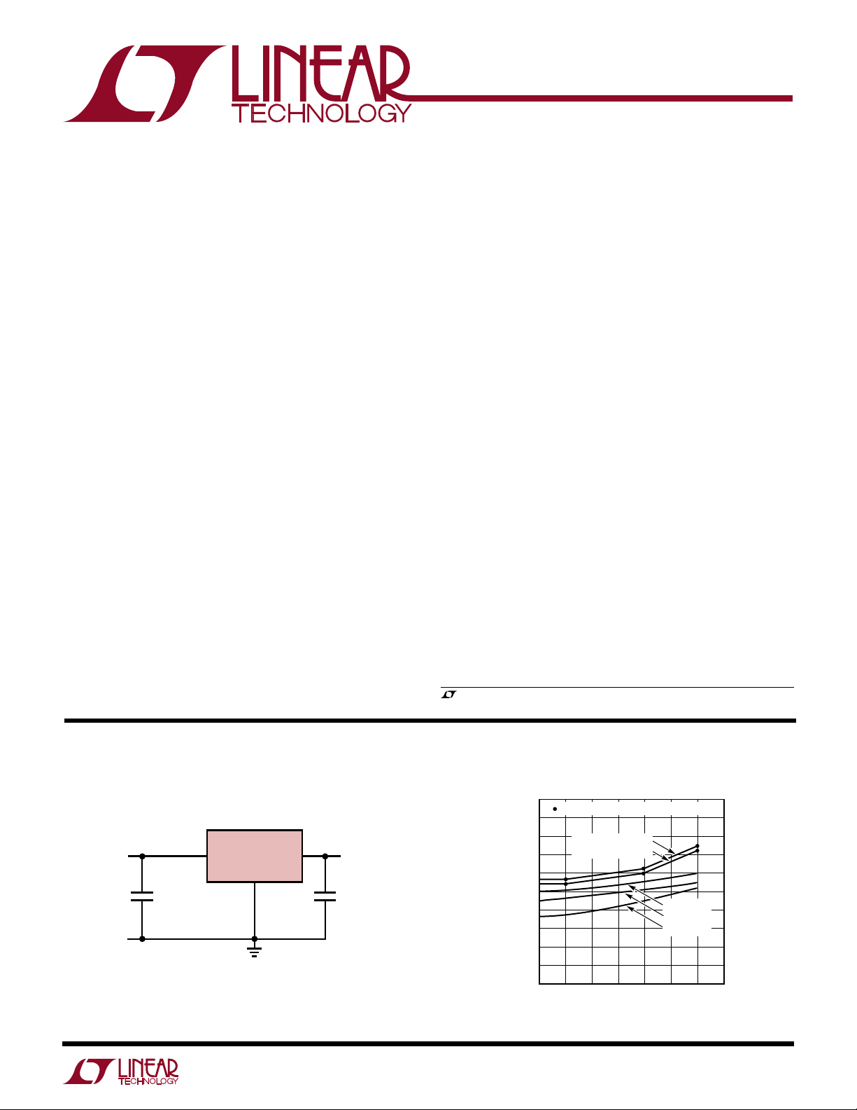
5V to 3.3V Regulator
V
≥ 4.75V 3.3V AT 1.5A
IN
10µF*
TANTALUM
LT1086-3.3
IN OUT
GND
LT1086 • TA01
10µF
TANTALUM
The LT1086 is pin compatible with older 3-terminal adjustable regulators. A 10µF output capacitor is required on
these new devices; however, this is usually included in
most regulator designs.
A 2.85V output version is offered for SCSI-2 active termination. For surface mount applications see the LT1117-
2.85 data sheet. For high current or lower dropout requirements see the LT1123-2.85 data sheet.
Unlike PNP regulators, where up to 10% of the output
current is wasted as quiescent current, the LT1086 quiescent current flows into the load, increasing efficiency.
, LTC and LT are registered trademarks of Linear Technology Corporation.
LT1086 Dropout Voltage
2
INDICATES GUARANTEED TEST POINT
–55°C ≤ TJ ≤ 150°C
1
0°C ≤ T
≤ 125°C
J
= –55°C
T
J
= 25°C
T
J
= 150°C
T
J
*MAY BE OMITTED IF INPUT SUPPLY IS WELL
BYPASSED WITHIN 2" OF THE LT1086
MINIMUM INPUT/OUTPUT DIFFERENTIAL (V)
0
0
0.5
OUTPUT CURRENT (A)
1
1.5
LT1086 • TA02
1
Page 2
LT1086 Series
WW
W
U
ABSOLUTE MAXIMUM RATINGS
Power Dissipation............................... Internally Limited
Input Voltage (Note 1) ............................................. 30V
Operating Input Voltage
Adjustable Devices ........................................... 25V
2.85V Devices .................................................. 18V
3.3V, 3.6V, and 5V Devices ............................... 20V
12V Devices ...................................................... 25V
Operating Junction Temperature Range
“C” Grades
Control Section ............................... 0°C to 125°C
Power Transistor............................. 0°C to 150°C
“I” Grades
Control Section .......................... –40°C to 125°C
Power Transistor........................ –40°C to 150°C
U
W
U
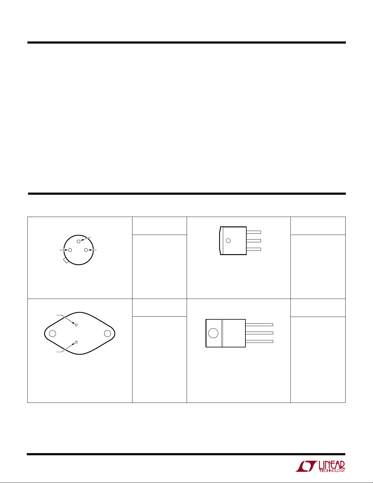
PACKAGE/ORDER INFORMATION
BOTTOM VIEW
V
IN
3-LEAD TO-39 METAL CAN
2
13
H PACKAGE
θJA = 150°C/W
ADJ
V
OUT
(CASE)
ORDER
PART NUMBER
LT1086CH
LT1086MH
“M” Grades
Control Section .......................... –55°C to 150°C
Power Transistor........................ –55°C to 200°C
Storage Temperature Range ................. – 65°C to 150°C
Lead Temperature (Soldering, 10 sec).................. 300°C
Note 1: Although the device’s maximum operating voltage is limited, (18V
for a 2.85V device, 20V for a 5V device, and 25V for adjustable and
12V devices) the devices are guaranteed to withstand transient input
voltages up to 30V. For input voltages greater than the maximum operating
input voltage some degradation of specifications will occur. For fixed
voltage devices operating at input/output voltage differentials greater than
15V, a minimum external load of 5mA is required to maintain regulation.
UUU
PRECONDITIONING
100% Thermal Shutdown Functional Test.
FRONT VIEW
3
TAB IS
OUTPUT
3-LEAD PLASTIC DD
θJA = 30°C/W**
** WITH PACKAGE SOLDERED TO 0.5IN2 COPPER AREA
OVER BACKSIDE GROUND PLANE OR INTERNAL POWER
PLANE. θ
DEPENDING ON MOUNTING TECHNIQUE.
CAN VARY FROM 20°C/W TO >40°C/W
JA
2
1
M PACKAGE
VIN
V
OUT
ADJ
(GND)*
ORDER
PART NUMBER
LT1086CM
LT1086CM-3.3
LT1086CM-3.6
LT1086IM
LT1086IM-3.3
LT1086IM-3.6
V
IN
ADJ (GND)*
2-LEAD TO-3 METAL CAN
*For fixed versions.
2
BOTTOM VIEW
2
1
K PACKAGE
θJA = 35°C/W
CASE
IS OUTPUT
ORDER
PART NUMBER
LT1086CK
LT1086CK-5
LT1086CK-12
LT1086IK
LT1086IK-5
LT1086IK-12
LT1086MK
LT1086MK-5
LT1086MK-12
TAB IS
OUTPUT
FRONT VIEW
3
2
1
T PACKAGE
3-LEAD PLASTIC TO-220
θJA = 50°C/W
VIN
V
OUT
ADJ
(GND)*
PART NUMBER
LT1086CT
LT1086CT-2.85
LT1086CT-3.3
LT1086IT
LT1086IT-5
LT1086IT-12
LT1086CT-3.6
LT1086CT-5
LT1086CT-12
ORDER
Page 3
LT1086 Series
ELECTRICAL CHARACTERISTICS
PARAMETER CONDITIONS MIN TYP MAX UNITS
Reference Voltage LT1086, LT1086H I
(Note 2) 10mA ≤ I
Output Voltage LT1086-2.85 I
(Note 2) 0V ≤ I
LT1086-3.3 VIN = 5V, I
LT1086-3.6 VIN = 5V, I
LT1086-5 I
LT1086-12 I
Line Regulation LT1086, LT1086H I
LT1086-2.85 I
LT1086-3.3 4.5V ≤ VIN ≤ 18V, I
LT1086-3.6 4.75V ≤ VIN ≤ 18V, I
LT1086-5 I
LT1086-12 I
Load Regulation LT1086, LT1086H (VIN – V
LT1086-2.85 VIN = 5V, 0 ≤ I
LT1086-3.3 VIN = 5V, 0 ≤ I
LT1086-3.6 VIN = 5.25V, 0 ≤ I
LT1086-5 VIN = 8V, 0 ≤ I
LT1086-12 VIN = 15V, 0 ≤ I
Dropout Voltage LT1086/-2.85/-3.3/-3.6/-5/-12 ∆V
– V
OUT
)
(V
IN
LT1086H ∆V
= 10mA, TJ = 25°C, (VIN – V
OUT
OUT
4.75V ≤ V
5V ≤ V
4.75V ≤ V
= 4.75V, I
V
IN
OUT
0 ≤ I
OUT
0 ≤ I
LOAD
OUT
OUT
OUT
≤ 1.5A, (0.5A for LT1086H), 1.5V ≤ (VIN – V
OUT
= 0mA, TJ = 25°C, VIN = 5V 2.82 2.85 2.88 V
≤ 1.5A, 4.35V ≤ VIN ≤ 18V ● 2.79 2.85 2.91 V
OUT
= 0mA, TJ = 25°C 3.267 3.300 3.333 V
OUT
≤ 18V, 0V ≤ I
IN
= 0mA, TJ = 25°C 3.564 3.600 3.636 V
OUT
≤ 18V, 0 ≤ I
IN
≤ 18V, 0 ≤ I
IN
OUT
OUT
≤ 1.5A ● 3.500 3.672 V
OUT
OUT
= 1.5A, TJ ≥ 0°C 3.300 3.672 V
= 0mA, TJ = 25°C, VIN = 8V 4.950 5.000 5.050 V
≤ 1.5A, 6.5V ≤ VIN ≤ 20V ● 4.900 5.000 5.100 V
OUT
= 0mA, TJ = 25°C, VIN = 15V 11.880 12.000 12.120 V
≤ 1.5A, 13.5V ≤ VIN ≤ 25V ● 11.760 12.000 12.240 V
OUT
= 10mA, 1.5V ≤ (VIN – V
= 0mA, TJ = 25°C, 4.35V ≤ VIN ≤ 18V 0.3 6 mV
= 0mA, TJ = 25°C 0.5 10 mV
OUT
= 0mA, TJ = 25°C 0.5 10 mV
OUT
= 0mA, TJ = 25°C, 6.5V ≤ VIN ≤ 20V 0.5 10 mV
= 0mA, TJ = 25°C, 13.5V ≤ VIN ≤ 25V 1.0 25 mV
) = 3V, 10mA ≤ I
OUT
) = 3V 1.238 1.250 1.262 V
OUT
) ≤ 15V ● 1.225 1.250 1.270 V
OUT
≤ 1.5A ● 3.235 3.300 3.365 V
≤ 1A, TJ ≥ 0°C 3.500 3.672 V
) ≤ 15V, TJ = 25°C 0.015 0.2 %
OUT
≤ 1.5A, (0.5A for LT1086H)
OUT
● 0.035 0.2 %
● 0.6 6 mV
● 1.0 10 mV
● 1.0 10 mV
● 1.0 10 mV
● 2.0 25 mV
TJ = 25°C (Notes 1, 2) 0.1 0.3 %
● 0.2 0.4 %
≤ 1.5A, TJ = 25°C (Notes 1, 2) 3 12 mV
= 5V, 0 ≤ I
V
IN
= 1%, I
REF
OUT
≤ 1.5A, TJ = 25°C (Notes 1, 2) 3 15 mV
OUT
≤ 1.5A, TJ = 25°C (Notes 1, 2) 3 15 mV
OUT
≤ 1A, TJ = 25°C 2 15 mV
OUT
≤ 1.5A, TJ = 25°C (Notes 1, 2) 5 20 mV
OUT
≤ 1.5A, TJ = 25°C (Notes 1, 2) 12 36 mV
OUT
, ∆V
OUT
OUT
= 1%, I
REF
= 0.5A (Note 3) ● 0.95 1.25 V
= 1.5A (Note 3) ● 1.3 1.5 V
OUT
● 620 mV
● 725 mV
● 625 mV
● 425 mV
● 10 35 mV
● 24 72 mV
3
Page 4
LT1086 Series
ELECTRICAL CHARACTERISTICS
PARAMETER CONDITIONS MIN TYP MAX UNITS
Current Limit LT1086/-2.85/-3.3/-3.6/-5/-12 (VIN – V
(V
IN
LT1086H (VIN – V
Minimum Load Current LT1086/LT1086H (VIN – V
(V
IN
– V
OUT
OUT
OUT
Quiescient Current LT1086-2.85 VIN ≤ 18V ● 510 mA
LT1086-3.3 V
LT1086-3.6 V
LT1086-5 V
≤ 18V ● 510 mA
IN
≤ 18V ● 510 mA
IN
≤ 20V ● 510 mA
IN
LT1086-12 VIN ≤ 25V ● 510 mA
Thermal Regulation TA = 25°C, 30ms pulse 0.008 0.04 %/W
Ripple Rejection f = 120Hz, C
LT1086, LT1086H C
LT1086-2.85 V
LT1086-3.3 V
LT1086-3.6 V
LT1086-5 V
= 25µF Tantalum, I
OUT
ADJ
= 6V ● 60 72 dB
IN
= 6.3V ● 60 72 dB
IN
= 6.6V ● 60 72 dB
IN
= 8V ● 60 68 dB
IN
= 25µF, (VIN – V
LT1083-12 VIN = 15V ● 54 60 dB
Adjust Pin Current LT1086, LT1086H TJ = 25°C55µA
Adjust Pin Current LT1086, LT1086H 10mA ≤ I
Change 1.5V ≤ (V
OUT
IN
Temperature Stability ● 0.5 %
Long Term Stability TA = 125°C, 1000 Hrs. 0.3 1 %
RMS Output Noise TA = 25°C, 10Hz = ≤ f ≤ 10kHz 0.003 %
OUT
)
(% of V
Thermal Resistance H Package: Control Circuitry/Power Transistor 15/20 °C/W
Junction-to-Case K Package: Control Circuitry/Power Transistor 1.7/4.0 °C/W
M Package: Control Circuitry/Power Transistor 1.5/4.0 °C/W
T Package: Control Circuitry/Power Transistor 1.5/4.0 °C/W
) = 5V ● 1.50 2.00 A
OUT
– V
) = 25V ● 0.05 0.15 A
OUT
) = 5V ● 0.50 0.700 A
) = 25V ● 0.02 0.075 A
) = 25V (Note 4) ● 510 mA
= 1.5A, (I
OUT
= 0.5A for LT1086H)
OUT
) = 3V ● 60 75 dB
OUT
●120 µA
≤ 1.5A, (0.5A for LT1086H)
– V
) ≤ 15V ● 0.2 5 µA
OUT
The ● denotes the specifications which apply over the full operating
temperature range.
Note 1: See thermal regulation specifications for changes in output voltage
due to heating effects. Line and load regulation are measured at a constant
junction temperature by low duty cycle pulse testing. Load regulation is
measured at the output lead ≈1/8" from the package.
Note 2: Line and load regulation are guaranteed up to the maximum power
dissipation of 15W (3W for the LT1086H). Power dissipation is determined
4
by the input/output differential and the output current. Guaranteed
maximum power dissipation will not be available over the full input/output
range. See Short-Circuit Current curve for available output current.
Note 3: Dropout voltage is specified over the full output current range of
the device. Test points and limits are shown on the Dropout Voltage curve.
Note 4: Minimum load current is defined as the minimum output current
required to maintain regulation. At 25V input/output differential the device
is guaranteed to regulate if the output current is greater than 10mA.
Page 5
W
CASE TEMPERATURE (°C)
*AS LIMITED BY MAXIMUM JUNCTION TEMPERATURE
50
POWER (W)
15
20
130
LT1086 • TPC06
10
5
0
70
90
110
150
120
60
80
100
140
LT1086MK
LT1086CK
LT1086CT
INPUT/OUTPUT DIFFERENTIAL (V)
0
0
MINIMUM OPERATING CURRENT (mA)
1
3
4
5
10
7
10
20
25
LT1086 • TPC03
2
8
9
6
5
15
30
35
TJ = 150°C
T
J
= 25°C
T
J
= –55°C
U
TYPICAL PERFORMANCE CHARACTERISTICS
LT1086 Short-Circuit Current
2.5
2.0
1.5
1.0
SHORT-CIRCUIT CURRENT (A)
0.5
0
0
TJ = 150°C
GUARANTEED
OUTPUT CURRENT
10 15 20
5
INPUT/OUTPUT DIFFERENTIAL (V)
Temperature Stability
2
1
0
–1
OUTPUT VOLTAGE CHANGE (%)
–2
–25
–50
0
50
25
TEMPERATURE (°C)
TJ = 25°C
= –55°C
T
J
75
25 30
LT1086 • TPC01
100
LT1086 • TPC04
125
150
0.10
∆I = 1.5A
0.05
0
–0.05
–0.10
–0.15
OUTPUT VOLTAGE DEVIATION (%)
–0.20
–50
050
–25 25
TEMPERATURE (°C)
Adjust Pin Current
100
90
80
70
60
50
40
30
ADJUST PIN CURRENT (µA)
20
10
0
–50
–25 25
0
50
TEMPERATURE (°C)
100
75
LT1086 • TPC02
125
100
75
LT1086 • TPC05
125
LT1086 Series
Minimum Operating Current
(Adjustable Device)LT1086 Load Regulation
150
LT1086 Maximum Power
Dissipation*
150
LT1086 Ripple Rejection
100
V
≤ 3V
90
80
70
60
50
40
30
RIPPLE REJECTION (dB)
20
10
0
10 1k 10k 100k
RIPPLE
(VIN – V
OUT
C
= 200µF AT FREQUENCIES < 60Hz
ADJ
= 25µF AT FREQUENCIES > 60Hz
C
ADJ
= 1.5A
I
OUT
100
P-P
(VIN – V
) ≥ V
DROPOUT
FREQUENCY (Hz)
V
RIPPLE
OUT
≤ 0.5V
) ≥ 3V
LT1086 • TPC07
P-P
LT1086 Ripple Rejection
vs Current
100
90
80
70
60
50
40
30
RIPPLE REJECTION (dB)
V
20
10
= 5V
OUT
= 25µF
C
ADJ
= 25µF
C
OUT
0
0
0.25
fR = 120Hz
V
fR = 20kHz
V
0.5
OUTPUT CURRENT (A)
≤ 3V
RIPPLE
≤ 0.5V
RIPPLE
0.75 1.0
P-P
P-P
1.25
LT1086 • TPC08
RIPPLE REJECTION (dB)
1.5
LT1086-5 Ripple Rejection
80
70
60
50
40
30
20
10
0
10 1k 10k 100k
(V
I
OUT
– V
IN
= 1.5A
V
≤ 3V
RIPPLE
) ≥ V
OUT
DROPOUT
100
FREQUENCY (Hz)
P-P
(VIN – V
V
RIPPLE
OUT
≤ 0.5V
) ≥ 3V
LT1086 • TPC09
P-P
5
Page 6

LT1086 Series
OUTPUT CURRENT (A)
0
0
RIPPLE REJECTION (dB)
20
30
40
50
60
70
0.1
0.2
0.3 0.4
LT1086 • TPC18
80
90
100
10
0.5
fR = 20kHz
V
RIPPLE
≤ 0.5V
P-P
V
OUT
= 5V
C
ADJ
= 25µF
C
OUT
= 25µF
fR = 120Hz
V
RIPPLE
≤ 3V
P-P
OUTPUT CURRENT (A)
0
0
RIPPLE REJECTION (dB)
20
30
40
50
60
70
0.25
0.5
0.75 1.0
LT1086 • TPC12
1.25
80
90
100
10
1.5
fR = 120Hz
V
RIPPLE
≤ 3V
P-P
fR = 20kHz
V
RIPPLE
≤ 0.5V
P-P
V
OUT
= 5V
C
ADJ
= 25µF
C
OUT
= 25µF
W
U
TYPICAL PERFORMANCE CHARACTERISTICS
LT1086-5 Ripple Rejection
vs Current
100
90
80
70
60
40
RIPPLE REJECTION (dB)
fR = 120Hz
≤ 3V
V
RIPPLE
fR = 20kHz
V
50
30
20
10
RIPPLE
V
= 5V
OUT
= 25µF
C
ADJ
= 25µF
C
OUT
0
0
0.25
P-P
≤ 0.5V
P-P
0.75 1.0
0.5
OUTPUT CURRENT (A)
LT1086 Line Transient Response
60
40
20
0
–20
DEVIATION (mV)
OUTPUT VOLTAGE
–40
V
OUT
I
OUT
–60
C
IN
C
OUT
14
13
12
DEVIATION (V)
11
INPUT VOLTAGE
0
C
= 1µF
ADJ
= 10V
= 0.2A
= 1µF TANTALUM
= 10µF TANTALUM
100
TIME (µs)
LT1086-12 Ripple Rejection
LT1086-12 Ripple Rejection
1.25
LT1086 • TPC10
1.5
80
70
60
50
40
30
RIPPLE REJECTION (dB)
20
10
0
10 1k 10k 100k
I
(V
OUT
– V
IN
= 1.5A
V
≤ 3V
RIPPLE
) ≥ V
OUT
DROPOUT
100
FREQUENCY (Hz)
P-P
(VIN – V
V
RIPPLE
OUT
≤ 0.5V
) ≥ 3V
LT1086 • TPC11
P-P
LT1086 Load Transient Response
0.3
0.2
0.1
0
= 0
C
ADJ
–0.1
DEVIATION (V)
OUTPUT VOLTAGE
–0.2
–0.3
C
= 1µF
ADJ
CIN = 1µF TANTALUM
= 10µF TANTALUM
C
OUT
1.5
1.0
0.5
200
LT1086 • TPC13
0
LOAD CURRENT (A)
0
V
V
PRELOAD = 100mA
50
TIME (µs)
C
OUT
IN
ADJ
= 10V
= 13V
= 0
100
LT1086 • TPC14
vs Current
LT1086H Short-Circuit Current
1.2
1.0
0.8
0.6
0.4
SHORT-CIRCUIT CURRENT (A)
0.2
0
0
GUARANTEED
OUTPUT CURRENT
5101520
INPUT/OUTPUT DIFFERENTIAL (V)
25
LT1086 • TPC15
2
1
MINIMUM INPUT/OUTPUT DIFFERENTIAL (V)
0
6
LT1086H Dropout Voltage
INDICATES GUARANTEED TEST POINT
0
0.1
OUTPUT CURRENT (A)
–55°C ≤ TJ ≤ 150°C
0°C ≤ T
0.2
≤ 125°C
J
TJ = –55°C
T
= 25°C
J
= 150°C
T
J
0.3
0.4
LT1086 • TPC16
LT1086H Load Regulation
0.10
∆I = 0.5A
0.05
0
–0.05
–0.10
–0.15
OUTPUT VOLTAGE DEVIATION (%)
–0.20
0.5
–50
050
–25 25
TEMPERATURE (°C)
LT1086H Ripple Rejection
vs Current
100
75
125
LT1086 • TPC17
150
Page 7

W
U
TYPICAL PERFORMANCE CHARACTERISTICS
100
V
≤ 3V
90
80
70
60
50
40
30
RIPPLE REJECTION (dB)
20
10
0
10 1k 10k 100k
RIPPLE
– V
(V
C
ADJ
C
ADJ
I
OUT
) ≥ V
IN
OUT
= 200µF AT FREQUENCIES < 60Hz
= 25µF AT FREQUENCIES > 60Hz
= 0.5A
100
FREQUENCY (Hz)
P-P
DROPOUT
V
RIPPLE
(VIN – V
OUT
≤ 0.5V
) ≥ 3V
LT1086 • TPC19
P-P
5
4
3
2
POWER (W)
1
0
*AS LIMITED BY MAXIMUM JUNCTION TEMPERATURE
LT1086H Maximum Power
Dissipation*LT1086H Ripple Rejection
LT1086MH
60
70
50
CASE TEMPERATURE (°C)
100
110
80
90
120
LT1086 Series
130
140
150
LT1086 • TPC20
BLOCK DIAGRAM
W
V
ADJ
THERMAL
LIMIT
V
IN
+
–
1086 • BD
V
OUT
7
Page 8

LT1086 Series
U
WUU
APPLICATIONS INFORMATION
The LT1086 family of 3-terminal regulators is easy to use
and has all the protection features that are expected in high
performance voltage regulators. They are short-circuit
protected, have safe area protection as well as thermal
shutdown to turn off the regulator should the temperature
exceed about 165°C at the sense point.
These regulators are pin compatible with older 3-terminal
adjustable devices, offer lower dropout voltage and more
precise reference tolerance. Further, the reference stability with temperature is improved over older types of
regulators. The only circuit difference between using the
LT1086 family and older regulators is that they require an
output capacitor for stability.
Stability
The circuit design used in the LT1086 family requires the
use of an output capacitor as part of the device frequency
compensation. For all operating conditions, the addition of
150µ F aluminum electrolytic or a 22µF solid tantalum on
the output will ensure stability. Normally capacitors much
smaller than this can be used with the LT1086. Many
different types of capacitors with widely varying characteristics are available. These capacitors differ in capacitor
tolerance (sometimes ranging up to ±100%), equivalent
series resistance, and capacitance temperature coefficient. The 150µ F or 22µ F values given will ensure stability.
When using the LT1086 the adjustment terminal can be
bypassed to improve ripple rejection. When the adjustment terminal is bypassed the requirement for an output
capacitor increases. The values of 22µ F tantalum or 150µ F
aluminum cover all cases of bypassing the adjustment
terminal. For fixed voltage devices or adjustable devices
without an adjust pin bypass capacitor, smaller output
capacitors can be used with equally good results and the
table below shows approximately what size capacitors are
needed to ensure stability.
Recommended Capacitor Values
INPUT OUTPUT ADJUSTMENT
10µF10µF Tantalum, 50µF Aluminum None
10µF22µF Tantalum, 150µF Aluminum 20µF
Normally, capacitor values on the order of 100µ F are used
in the output of many regulators to ensure good transient
response with heavy load current changes. Output capacitance can be increased without limit and larger values of
output capacitor further improve stability and transient
response of the LT1086 regulators.
Another possible stability problem that can occur in monolithic IC regulators is current limit oscillations. These can
occur because in current limit, the safe area protection
exhibits a negative impedance. The safe area protection
decreases the current limit as the input-to-output voltage
increases.That is the equivalent of having a negitive resistance since increasing voltage causes current to decrease.
Negative resistance during current limit is not unique to
the LT1086 series and has been present on all power IC
regulators. The value of negative resistance is a function of
how fast the current limit is folded back as input-to-output
voltage increases. This negative resistance can react with
capacitors or inductors on the input to cause oscillation
during current limiting. Depending on the value of series
resistance, the overall circuitry may end up unstable. Since
this is a system problem, it is not necessarily easy to solve;
however it does not cause any problems with the IC
regulator and can usually be ignored.
Protection Diodes
In normal operation the LT1086 family does not need any
protection diodes. Older adjustable regulators required
protection diodes between the adjustment pin and the
output and from the output to the input to prevent overstressing the die. The internal current paths on the LT1086
adjustment pin are limited by internal resistors. Therefore,
even with capacitors on the adjustment pin, no protection
diode is needed to ensure device safety under short-circuit
conditions.
Diodes between input and output are usually not needed.
The internal diode between the input and the output pins
of the LT1086 family can handle microsecond surge
currents of 10A to 20A. Even with large output capacitances, it is very difficult to get those values of surge
currents in normal operation. Only with high value output
capacitors such as 1000µ F to 5000µF, and with the input
pin instantaneously shorted to ground, can damage occur.
A crowbar circuit at the input of the LT1086 can generate
those kinds of currents and a diode from output to input is
then recommended. Normal power supply cycling or even
8
Page 9

LT1086 Series
R1
10µF
TANTALUM
R2
IN OUT
I
ADJ
50µA
ADJ
V
OUT
LT1086
V
IN
1086 • F01
V
REF
V
OUT
= V
REF
1 + + I
ADJ
R2
R2
R1
( )
+
U
WUU
APPLICATIONS INFORMATION
plugging and unplugging in the system will not generate
current large enough to do any damage.
The adjustment pin can be driven on a transient basis
±25V, with respect to the output without any device
degradation. Of course as with any IC regulator, exceeding
the maximum input-to-output voltage differential causes
the internal transistors to break down and none of the
protection circuitry is functional.
D1
1N4002
(OPTIONAL)
VIN V
LT1086
IN OUT
ADJ
+
C
ADJ
10µF
C
OUT
150µF
LT1086 • AI01
OUT
+
R1
R2
Overload Recovery
Like any of the IC power regulators, the LT1086 has safe
area protection. The safe area protection decreases the
current limit as input-to-output voltage increases and
keeps the power transistor inside a safe operating region
for all values of input-to-output voltage. The LT1086
protection is designed to provide some output current at
all values of input-to-output voltage up to the device
breakdown.
When power is first turned on, as the input voltage rises,
the output follows the input, allowing the regulator to start
up into very heavy loads. During the start-up, as the input
voltage is rising, the input-to-output voltage differential
remains small, allowing the regulator to supply large
output currents. With high input voltage, a problem can
occur wherein removal of an output short will not allow the
output voltage to recover. Older regulators such as the
7800 series also exhibited this phenomenon, so it is not
unique to the LT1086.
the power supply may need to be cycled down to zero and
brought up again to make the output recover.
Ripple Rejection
For the LT1086 the typical curves for ripple rejection
reflect values for a bypassed adjust pin. This curve will be
true for all values of output voltage. For proper bypassing
and ripple rejection approaching the values shown, the
impedance of the adjust pin capacitor at the ripple frequency should equal the value of R1, (normally 100Ω to
120Ω). The size of the required adjust pin capacitor is a
function of the input ripple frequency. At 120Hz the adjust
pin capacitor should be 13µ F if R1 = 100Ω. At 10kHz only
0.16µ F is needed.
For circuits without an adjust pin bypass capacitor the
ripple rejection will be a function of output voltage. The
output ripple will increase directly as a ratio of the output
voltage to the reference voltage (V
ample, with the output voltage equal to 5V and no adjust
pin capacitor, the output ripple will be higher by the ratio
of 5V/1.25V or four times larger. Ripple rejection will be
degraded by 12dB from the value shown on the LT1086
curve. Typical curves are provided for the 5V and 12V
devices since the adjust pin is not available.
Output Voltage
The LT1086 develops a 1.25V reference voltage between
the output and the adjust terminal (see Figure 1). By
placing a resistor R1 between these two terminals, a
constant current is caused to flow through R1 and down
through R2 to set the overall output voltage. Normally this
current is chosen to be the specified minimum load
current of 10mA. Because I
when compared with the current through R1, it represents a small error and can usually be ignored. For fixed
voltage devices R1 and R2 are included in the device.
OUT/VREF
is very small and constant
ADJ
). For ex-
The problem occurs with a heavy output load when the
input voltage is high and the output voltage is low, such as
immediately after a removal of a short. The load line for
such a load may intersect the output current curve at two
points. If this happens there are two stable output operating points for the regulator. With this double intersection
Figure 1. Basic Adjustable Regulator
9
Page 10

LT1086 Series
U
WUU
APPLICATIONS INFORMATION
Load Regulation
Because the LT1086 is a 3-terminal device, it is not
possible to provide true remote load sensing. Load regulation will be limited by the resistance of the wire connecting the regulator to the load. The data sheet specification
for load regulation is measured at the bottom of the
package. Negative side sensing is a true Kelvin connection, with the bottom of the output divider returned to the
negative side of the load. Although it may not be immediately obvious, best load regulation is obtained when the
top of the resistor divider R1 is connected
case
not to the load
. This is illustrated in Figure 2. If R1
were connected to the load, the effective resistance between the regulator and the load would be:
R2 + R1
RP , RP = Parasitic Line Resistance
()
R1
R
P
PARASITIC
IN
Figure 2. Connections for Best Load Regulation
LT1086 OUTINV
ADJ
*CONNECT R1 TO CASE
CONNECT R2 TO LOAD
LINE RESISTANCE
R1*
R2*
Connected as shown RP is not multiplied by the divider
ratio. RP is about 0.004Ω per foot using 16-gauge wire.
This translates to 4mV/ft at 1A load current, so it is
important to keep the positive lead between regulator and
load as short as possible and use large wire or PC board
traces.
Note that the resistance of the package leads for the H
package ≈0.06Ω/inch. While it is usually not possible to
connect the load directly to the package, it is possible to
connect larger wire or PC traces close to the case to avoid
voltage drops that will degrade load regulation.
For fixed voltage devices the top of R1 is internally Kelvin
connected and the ground pin can be used for negative
side sensing.
directly
R
1086 • F02
to the
L
Thermal Considerations
The LT1086 series of regulators have internal power and
thermal limiting circuitry designed to protect the device
under overload conditions. For continuous normal load
conditions however, maximum junction temperature ratings must not be exceeded. It is important to give careful
consideration to all sources of thermal resistance from
junction to ambient. This includes junction-to-case, caseto-heat sink interface and heat sink resistance itself. New
thermal resistance specifications have been developed to
more accurately reflect device temperature and ensure
safe operating temperatures. The data section for these
new regulators provides a separate thermal resistance and
maximum junction temperature for both the
tion
and the
Power Transistor
. Previous regulators, with a
Control Sec-
single junction-to-case thermal resistance specification,
used an average of the two values provided here and
therefore could allow excessive junction temperatures
under certain conditions of ambient temperature and heat
sink resistance. To avoid this possibility, calculations
should be made for both sections to ensure that both
thermal limits are met.
For example, using a LT1086CK (TO-3, Commercial) and
assuming:
VIN(max continuous) = 9V, V
TA = 75°C, θ
θ
CASE-TO-HEAT SINK
HEAT SINK
= 3°C/W,
= 0.2°C/W for K package with
OUT
= 5V, I
OUT
= 1A,
thermal compound.
Power dissipation under these conditions is equal to:
PD = (VIN – V
OUT
)(I
OUT
) = 4W
Junction temperature will be equal to:
TJ = TA + PD (θ
HEAT SINK
+ θ
CASE-TO-HEAT SINK
+ θJC)
For the Control Section:
TJ = 75°C + 4W(3°C/W + 0.2°C/W + 0.7°C/W) = 95°C
95°C < 125°C = T
(Control Section
JMAX
Commercial Range)
For the Power Transistor:
TJ = 75°C + 4W(3°C/ W + 0.2°C/W + 4 °C/ W) = 103.8°C
103.8°C < 150°C = T
(Power Transistor
JMAX
Commercial Range)
10
Page 11

LT1086 Series
V
IN
≥ 6.5V 5V AT 1.5A
*REQUIRED FOR STABILITY
LT1086
LT1086 • AI02
10µF*
TANTALUM
121Ω
1%
365Ω
1%
10µF
IN OUT
ADJ
+
+
U
WUU
APPLICATIONS INFORMATION
In both cases the junction temperature is below the
maximum rating for the respective sections, ensuring
reliable operation.
Junction-to-case thermal resistance for the K and T packages is specified from the IC junction to the bottom of the
case directly below the die. This is the lowest resistance
path for heat flow. While this is also the lowest resistance
path for the H package, most available heat sinks for this
package are of the clip-on type that attach to the cap of the
package. The data sheet specification for thermal resistance for the H package is therefore written to reflect this.
U
TYPICAL APPLICATIONS
5V, 1.5A Regulator
In all cases proper mounting is required to ensure the best
possible heat flow from the die to the heat sink. Thermal
compound at the case-to-heat sink interface is strongly
recommended. In the case of the H package, mounting the
device so that heat can flow out the bottom of the case will
significantly lower thermal resistance (≈ a factor of 2). If
the case of the device must be electrically isolated, a
thermally conductive spacer can be used as long as its
added contribution to thermal resistance is considered.
Note that the case of all devices in this series is electrically
connected to the output.
1N5817
+ +
10µF
TANTALUM
4.25V
TO 5.25V
SCSI-2 Active Termination
LT1086-2.85IN OUT
GND
TERMPWR
10µF
TANTALUM
0.1µF
CERAMIC
18 TOTAL
110Ω
2%
110Ω
2%
110Ω
2%
110Ω
110Ω
110Ω
LT1086 • TA03
11
Page 12

LT1086 Series
IN
V
IN
OUT
TTL
ADJ
1k
1k
10µF
100µF
5V
LT1086
2N3904
LT1086 • TA05
+
121Ω
1%
365Ω
1%
+
TYPICAL APPLICATIONS
U
1.2V to 15V Adjustable Regulator
V
IN
IN OUT
LT1086
ADJ
+
C1*
10µF
*NEEDED IF DEVICE IS FAR FROM FILTER CAPACITORS
†
V
= 1.25V 1 +
OUT
(
R2
5k
R2
)
R1
Battery Charger
I
LT1086
IN
V
IN
R2
1 +V
– 1.25
OUT
=
I
F
dIF
()
dV
OUT
()
R1
R2
1 + – R
S
()
R1
1
=
R2
1 + – R
S
()
R1
ADJ
1.25V
R2
R
OUT
R1
LT1086 • TA06
R1
121Ω
F
S
5V Regulator with Shutdown
†
V
OUT
+
C2
100µF
LT1086 • TA04
Adjusting Output Voltage of Fixed Regulators
> 12V 5V TO 10V
V
OUT
V
IN
+ +
IN OUT
LT1086-5
10µF
10µF*
*OPTIONAL IMPROVES RIPPLE REJECTION
GND
+
1k
100µF
LT1086 • TA07
Regulator with Reference Protected High Current Lamp Driver
> 11.5V 10V
V
IN
10µF
LT1086-5
IN OUT
GND
5V
LT1029
++
100µF
LT1086 • TA08
TTL OR
CMOS
10k
LT1086
ADJ
INOUT
15V
12V
1A
LT1086 • TA10
Remote Sensing
R
P
V
IN
+
RETURN
10µF
LT1086 OUTIN
ADJ
100µF
25Ω
121Ω
365Ω
(MAX DROP 300mV)
+
V
IN
7
6
LM301A
1
100pF
2
–
1k
3
+
8
5µF
4
+
25Ω
V
5V
R
L
RETURN
LT1086 • TA09
OUT
12
Page 13

U
TYPICAL APPLICATIONS
HEAT SINK
2N6667
DARLINGTON
+
MDA201
–
MBR360
Q1
10k
+
4700µF
High Efficiency Dual Linear Supply
L1
285µH
1000µF
++
1k
510k
8
7
LT1011
4
2.4k
2
+
3
–
LT1086
IN OUT
30k
20k*
ADJ
LT1004-2.5
30.1k*
LT1086 Series
12V
124Ω*
+
100µF
1.07k*
1.5A
D1
1N4002
130VAC
TO 90VAC
STANCOR
P-8685
DARLINGTON
HEAT SINK
2N6667
Q2
+
MDA201
+
–
*1% FILM RESISTORS
MDA = MOTOROLA
L1 = PULSE ENGINEERING, INC. #PE-92106
MBR360
10k
4700µF
1k
FEEDBACK PATH
L1
285µH
1000µF
7
510k
8
LT1011
4
2.4k
30k
2
+
3
–
IN OUT
High Efficiency Dual Supply
MUR410
5V OUTPUT
(TYPICAL)
+
470µF
LT1086
ADJ
LT1004-2.5
20k*
30.1k*
124Ω*
1.07k*
+
100µF
LT1086 • TA11
D2
1N4002
–12V
1.5A
V
IN
SWITCHING
REGULATOR
*1% FILM RESISTORS
MUR410
MUR410
IN OUT
+
470µF
IN OUT
+
470µF
LT1086
ADJ
+
LT1086
ADJ
+
10µF
10µF
124Ω*
1.07k*
124Ω*
1.07k*
12V
1.5A
+
10µF
+
10µF
LT1086 • TA12
1N4002
1N4002
–12V
1.5A
13
Page 14

LT1086 Series
R1
121Ω
1%
IN OUT
ADJ
R2
365Ω
1%
10µF
V
IN
≥ 6.5V
LT1086
V
OUT
= 5V
LT1086 • TA14
+
C1
10µF*
150µF
+
*C1 IMPROVES RIPPLE REJECTION.
XC SHOULD BE ≈ R1 AT RIPPLE FREQUENCY
IN
OUT
GND
10,000µF
LT1086-12
LT1086 • TA16
100µF
V
OUT
= –12V
FLOATING INPUT
V
IN
+ +
TYPICAL APPLICATIONS
U
V
IN
V
Battery Backed Up Regulated Supply
IN OUT
+
SELECT FOR
CHARGE RATE
+
10µF
10µF6.5V
LT1086-5
GND
IN OUT
LT1086-5
GND
Automatic Light Control Low Dropout Negative Supply
IN
IN
LT1086
+
10µF
OUT
ADJ
50Ω
1.2k
+
5.2V LINE
5V BATTERY
100µF
LT1086 • TA13
100µF
LT1086 • TA15
Improving Ripple Rejection
PACKAGE DESCRIPTION
REFERENCE
PLANE
*
14
LEAD DIAMETER IS UNCONTROLLED BETWEEN THE REFERENCE PLANE
AND 0.045" BELOW THE REFERENCE PLANE
**
FOR SOLDER DIP LEAD FINISH, LEAD DIAMETER IS
0.350 – 0.370
(8.890 – 9.398)
0.305 – 0.335
(7.747 – 8.509)
0.050
(1.270)
MAX
0.016 – 0.019**
(0.406 – 0.483)
DIA
U
Dimensions in inches (millimeters) unless otherwise noted.
H Package
3-Lead TO-39 Metal Can
(LTC DWG # 05-08-1330)
0.200
(5.080)
TYP
PIN 1
45°
0.165 – 0.185
(4.191 – 4.699)
*
(12.700)
0.016 – 0.024
(0.406 – 0.610)
0.500
MIN
0.029 – 0.045
(0.737 – 1.143)
0.028 – 0.034
(0.711 – 0.864)
0.100
(2.540)
0.100
(2.540)
H3(TO-39) 1197
Page 15

PACKAGE DESCRIPTION
0.320 – 0.350
(8.13 – 8.89)
0.420 – 0.480
(10.67 – 12.19)
0.760 – 0.775
(19.30 – 19.69)
0.038 – 0.043
(0.965 – 1.09)
U
Dimensions in inches (millimeters) unless otherwise noted.
K Package
2-Lead TO-3 Metal Can
(LTC DWG # 05-08-1310)
1.177 – 1.197
(29.90 – 30.40)
0.210 – 0.220
(5.33 – 5.59)
0.067 – 0.077
(1.70 – 1.96)
0.495 – 0.525
(12.57 – 13.34)
0.060 – 0.135
(1.524 – 3.429)
0.425 – 0.435
(10.80 – 11.05)
LT1086 Series
0.655 – 0.675
(16.64 – 17.15)
0.151 – 0.161
(3.86 – 4.09)
DIA, 2PLCS
0.167 – 0.177
(4.24 – 4.49)
R
R
K2 (TO-3) 0695
0.256
(6.502)
0.060
(1.524)
0.300
(7.620)
BOTTOM VIEW OF DD PAK
HATCHED AREA IS SOLDER PLATED
COPPER HEAT SINK
0.060
(1.524)
0.075
(1.905)
0.183
(4.648)
M Package
3-Lead Plastic DD Pak
(LTC DWG # 05-08-1460)
0.060
(1.524)
TYP
0.330 – 0.370
(8.382 – 9.398)
+0.012
0.143
–0.020
+0.305
3.632
()
–0.508
0.050
(1.270)
TYP
0.390 – 0.415
(9.906 – 10.541)
15° TYP
0.090 – 0.110
(2.286 – 2.794)
0.165 – 0.180
(4.191 – 4.572)
0.059
(1.499)
TYP
0.013 – 0.023
(0.330 – 0.584)
0.045 – 0.055
(1.143 – 1.397)
+0.008
0.004
–0.004
+0.203
0.102
()
–0.102
0.095 – 0.115
(2.413 – 2.921)
0.050 ± 0.012
(1.270 ± 0.305)
M (DD3) 0396
Information furnished by Linear Technology Corporation is believed to be accurate and reliable.
However, no responsibility is assumed for its use. Linear Technology Corporation makes no representation that the interconnection of its circuits as described herein will not infringe on existing patent rights.
15
Page 16

LT1086 Series
PACKAGE DESCRIPTION
U
Dimensions in inches (millimeters) unless otherwise noted.
T Package
3-Lead Plastic TO-220
(LTC DWG # 05-08-1420)
0.980 – 1.070
(24.892 – 27.178)
RELATED PARTS
0.390 – 0.415
(9.906 – 10.541)
0.460 – 0.500
(11.684 – 12.700)
0.520 – 0.570
(13.208 – 14.478)
0.090 – 0.110
(2.286 – 2.794)
0.028 – 0.038
(0.711 – 0.965)
0.147 – 0.155
(3.734 – 3.937)
0.230 – 0.270
(5.842 – 6.858)
(14.478 – 15.748)
0.330 – 0.370
(8.382 – 9.398)
0.218 – 0.252
(5.537 – 6.401)
0.050
(1.270)
TYP
DIA
0.570 – 0.620
0.165 – 0.180
(4.191 – 4.572)
0.013 – 0.023
(0.330 – 0.584)
0.045 – 0.055
(1.143 – 1.397)
0.095 – 0.115
(2.413 – 2.921)
T3 (TO-220) 1197
PART NUMBER DESCRIPTION COMMENTS
LT1528 3A Low Dropout Regulator 0.55V Dropout for 5V to 4V Regulation
LT1587 3A Low Dropout Regulator Fast Transient Response Reduces Decoupling Capacitance
1086fe LT/GP 0398 2K REV E • PRINTED IN USA
© LINEAR TECHNOLOGY CORPORATION 1988
16
Linear Technology Corporation
1630 McCarthy Blvd., Milpitas, CA 95035-7417 ● (408) 432-1900
FAX: (408) 434-0507
●
TELEX: 499-3977 ● www.linear-tech.com
 Loading...