

Datasheet LT1085MK-5, LT1085IM-3.6, LT1085CK-12, LT1084MK-5, LT1084CT-5 Datasheet (Linear Technology)
...Page 1
FEATURES
■
Three-Terminal 3.3V, 3.6V, 5V and 12V
■
Output Current of 3A, 5A or 7.5A
■
Operates Down to 1V Dropout
■
Guaranteed Dropout Voltage at Multiple Current Levels
■
Line Regulation: 0.015%
■
Load Regulation: 0.1%
■
100% Thermal Limit Functional Test
■
Adjustable Versions Available
U
APPLICATIO S
■
High Efficiency Linear Regulators
■
Post Regulators for Switching Supplies
■
Constant Current Regulators
■
Battery Chargers
DEVICE OUTPUT CURRENT*
LT1083 7.5 Amps
LT1084 5.0 Amps
LT1085 3.0 Amps
*For a 1.5A low dropout regulator see the LT1086 data sheet.
LT1083/LT1084/LT1085 Fixed
3A, 5A, 7.5A Low Dropout
Positive Fixed Regulators
U
DESCRIPTIO
The LT®1083 series of positive adjustable regulators are
designed to provide 3A, 5A and 7.5A with higher efficiency
than currently available devices. All internal circuitry is
designed to operate down to 1V input to output differential
and the dropout voltage is fully specified as a function of
load current. Dropout is guaranteed at a maximum of 1.5V
at maximum output current, decreasing at lower load
currents. On-chip trimming adjusts the output voltage to
1%. Current limit is also trimmed, minimizing the stress
on both the regulator and power source circuitry under
overload conditions.
The LT1083 series devices are pin compatible with older
three-terminal regulators. A 10µF output capacitor is
required on these new devices; however, this is usually
included in most regulator designs.
Unlike PNP regulators, where up to 10% of the output
current is wasted as quiescent current, the LT1083 quiescent current flows into the load, increasing efficiency.
, LTC and LT are registered trademarks of Linear Technology Corporation.
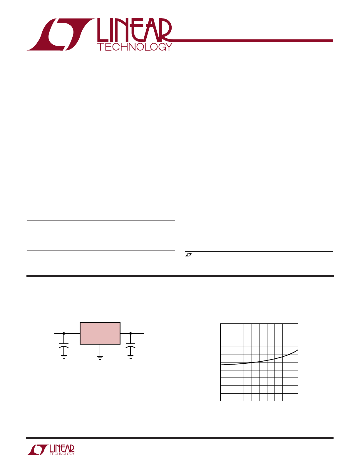
U
TYPICAL APPLICATIO
5V, 7.5A Regulator
VIN ≥ 6.5V 5V AT 7.5A
+
10µF
LT1083-5
*REQUIRED FOR STABILITY
+
22µF*
TANTALUM
LT1083/4/5 TA01
Dropout Voltage vs Output Current
2
1
INPUT/OUTPUT VOLTAGE DIFFERENTIAL (V)
0
0
I
/2
FULLLOAD
OUTPUT CURRENT (A)
I
FULLLOAD
1083/4/5 TA02
1
Page 2
LT1083/LT1084/LT1085 Fixed
WWWU
ABSOLUTE AXI U RATI GS
(Note 1)
Power Dissipation.............................. Internally Limited
Input Voltage* ........................................................ 30V
Operating Input Voltage
3.3V, 3.6V Devices ........................................... 20V
5V Devices ....................................................... 20V
12V Devices ..................................................... 25V
Operating Junction Temperature Range
“C” Grades
Control Section .............................. 0°C to 125°C
Power Transistor............................ 0°C to 150°C
“M” Grades
Control Section .......................... –55°C to 150°C
Power Transistor........................ –55°C to 200°C
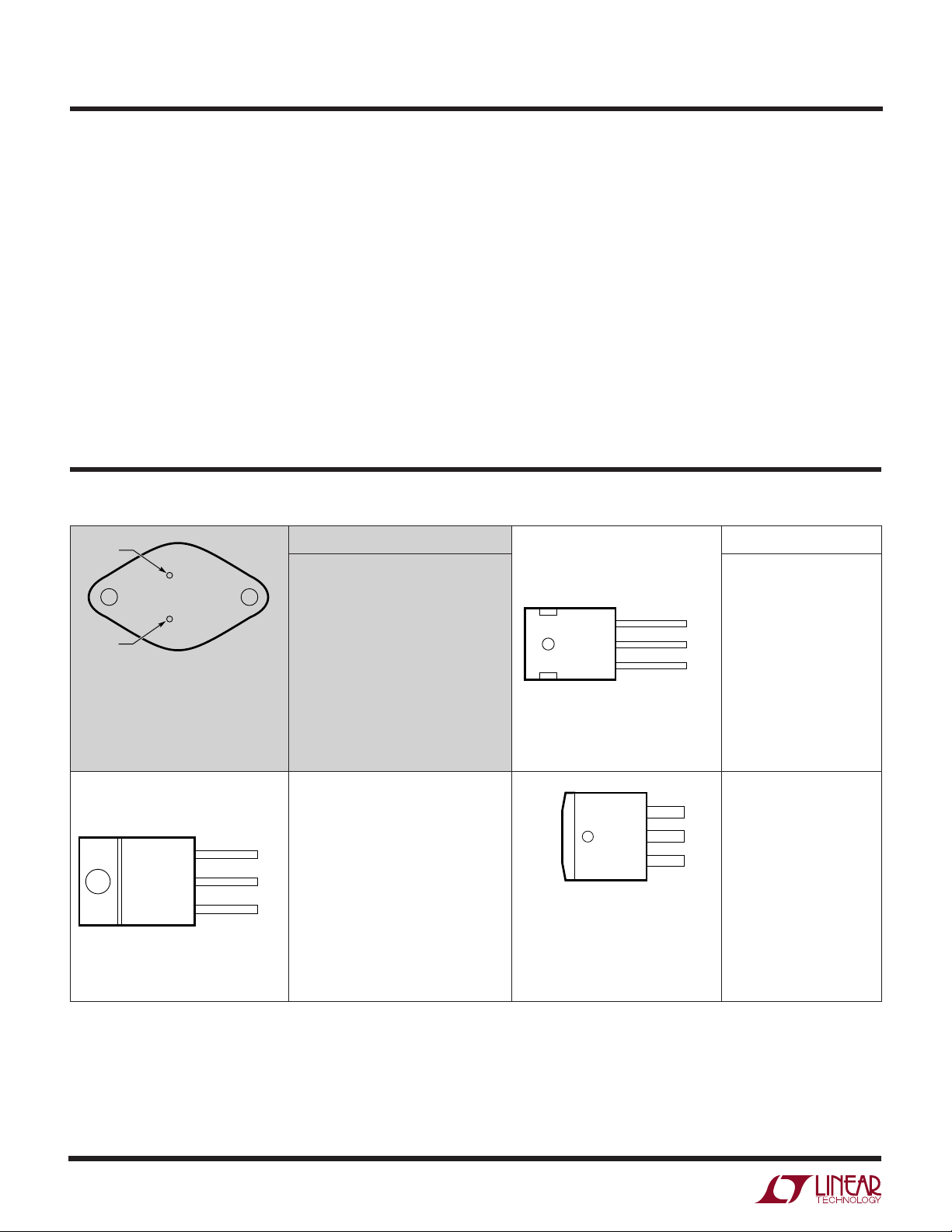
UU
W
PACKAGE/ORDER I FOR ATIO
V
IN
GND
2-LEAD TO-3 METAL CAN
2
1
K PACKAGE
θJA = 35°C/W
CASE IS
OUTPUT
ORDER PART NUMBER
LT1083CK-5
LT1083CK-12
LT1083MK-5
LT1083MK-12
LT1084CK-5
LT1084CK-12
LT1084MK-5
LT1084MK-12
LT1085CK-5
LT1085CK-12
LT1085MK-5
LT1085MK-12
OBSOLETE NOT RECOMMENDED
Storage Temperature Range ................ –65°C to 150°C
Lead Temperature (Soldering, 10 sec)................. 300°C
*Although the devices maximum operating voltage is limited, (20V for a
3V, 5V device, and 25V for a 12V device) the devices are guaranteed to
withstand transient input voltages up to 30V. For input voltages greater
than the maximum operating input voltage some degradation of
specifications will occur. For input/output voltage differentials greater than
15V, a minimum external load of 5mA is required to maintain regulation.
U
UU
PRECO DITIO I G
100% Thermal Limit Functional Test.
ORDER PART NUMBER
TAB IS
OUTPUT
FRONT VIEW
3
2
1
P PACKAGE
3-LEAD TO-3P PLASTIC
θJA = 45°C/W
V
V
GND
IN
OUT
LT1083CP-5
LT1083CP-12
LT1084CP-5
LT1084CP-12
FOR NEW DESIGNS
TAB IS
OUTPUT
Consult factory for parts specified with wider operating temperature ranges.
FRONT VIEW
3
2
1
T PACKAGE
3-LEAD PLASTIC TO-220
= 50°C/W
θ
JA
V
IN
V
OUT
GND
LT1084CT-3.3
LT1084CT-5
LT1084CT-12
LT1085CT-3.3
LT1085CT-3.6
LT1085CT-5
LT1085CT-12
2
FRONT VIEW
3
TAB IS
OUTPUT
3-LEAD PLASTIC DD
*WITH PACKAGE SOLDERED TO 0.52IN
COPPER AREA OVER BACKSIDE GROUND
PLANE OR INTERNAL POWER PLANE. θ
VARY FROM 20°C/W TO > 40°C/W DEPENDING
ON MOUNTING TECHNIQUE.
2
1
M PACKAGE
θJA = 30°C/W*
V
V
GND
2
JA
IN
OUT
CAN
LT1085CM-3.3
LT1085CM-3.6
LT1085IM-3.6
Page 3
LT1083/LT1084/LT1085 Fixed
ELECTRICAL CHARACTERISTICS
The ● denotes the specifications which apply over the full operating
temperature range, otherwise specifications are at TA = 25°C.
PARAMETER CONDITIONS MIN TYP MAX UNITS
Output Voltage LT1084-3.3 I
LT1085-3.3 VIN = 5V, I
LT1085-3.6 VIN = 5V, I
LT1085-3.6 5V ≤ VIN ≤ 15V, 0 ≤ I
LT1083/4/5-5 I
LT1083/4/5-12 I
Line Regulation LT1084-3.3 I
LT1085-3.3 4.8V ≤ VIN ≤ 15V, I
LT1085-3.6 4.8V ≤ VIN ≤ 15V, I
LT1083/4/5-5 I
LT1083/4/5-12 I
Load Regulation LT1084-3.3 VIN = 5V, 0 ≤ I
LT1085-3.3 VIN = 5V, 0 ≤ I
LT1085-3.6 VIN = 5.25V, 0 ≤ I
LT1083/4/5-5 VIN = 8V, 0 ≤ I
LT1083/4/5-12 VIN = 15V, 0 ≤ I
Dropout Voltage LT1084/5-3.3 ∆V
LT1085-3.6 ∆V
LT1083/4/5-5 ∆V
LT1083/4/5-12 ∆V
Current Limit LT1083-5 VIN = 10V ● 8.0 9.5 A
LT1083-12 VIN = 17V ● 8.0 9.5 A
LT1084-3.3 VIN = 8V ● 5.5 6.5 A
LT1084-5 VIN = 10V ● 5.5 6.5 A
LT1084-12 VIN = 17V ● 5.5 6.5 A
LT1085-3.3/3.6 VIN = 8V ● 3.2 4.0 A
LT1085-5 VIN = 10V ● 3.2 4.0 A
LT1085-12 VIN = 17V ● 3.2 4.0 A
= 0mA, TJ = 25°C, VIN = 8V (K Package Only) 3.270 3.300 3.330 V
OUT
4.8V ≤ VIN ≤ 15V, 0 ≤ I
= 0mA, TJ = 25°C (K Package Only) 3.270 3.300 3.330 V
4.8V ≤ V
5V ≤ V
OUT
≤ 15V, 0 ≤ I
IN
= 0mA, TJ = 25°C (K Package Only) 3.564 3.600 3.636 V
OUT
≤ 15V, 0 ≤ I
IN
5V ≤ VIN ≤ 15V, 0 ≤ I
VIN = 4.75V, I
V
= 4.75V, I
IN
VIN = 4.75V, I
= 0mA, TJ = 25°C, VIN = 8V (K Package Only) 4.950 5.000 5.050 V
OUT
0 ≤ I
≤ I
OUT
= 0mA, TJ = 25°C, VIN = 15V (K Package Only) 11.880 12.000 12.120 V
OUT
0 ≤ I
≤ I
OUT
= 0mA, TJ = 25°C, 4.8V ≤ VIN ≤ 15V 0.5 6 mV
OUT
= 0mA, TJ = 25°C, 6.5V ≤ VIN ≤ 20V (Notes 2, 3) 0.5 10 mV
OUT
= 0mA, TJ = 25°C, 13.5V ≤ VIN ≤ 25V (Notes 2, 3) 1.0 25 mV
OUT
= 33mV, I
OUT
= 36mV, I
OUT
= 50mV, I
OUT
= 120mV, I
OUT
= 3A, TJ ≥ 0°C 3.350 3.672 V
OUT
= 2.5A, TJ ≥ 0°C 3.450 3.672 V
OUT
= 1.5A, TJ > 0°C 3.528 3.672 V
OUT
FULLOAD
FULLOAD
OUT
OUT
OUT
OUT
OUT
OUT
OUT
OUT
≤ I
OUT
≤ I
OUT
≤ I
OUT
FULLOAD
≤ I
OUT
FULLOAD
≤ 2.5A (Notes 3, 4, 9) ● 3.528 3.672 V
OUT
(Notes 3, 4, 9) ● 3.235 3.300 3.365 V
FULLOAD
(Notes 3, 4, 9) ● 3.235 3.300 3.365 V
FULLOAD
(Note 9) ● 3.500 3.672 V
, TJ ≥ 0°C (Notes 3, 4, 9) 3.528 3.672 V
, 6.5V ≤ VIN ≤ 20V (Notes 4, 6, 7, 9) 4.900 5.000 5.100 V
, 13.5V ≤ VIN ≤ 25V (Notes 4, 6, 7, 9) 11.760 12.000 12.240 V
● 1.0 6 mV
= 0mA, TJ= 25°C 0.5 6 mV
OUT
= 0mA, TJ= 25°C 0.5 6 mV
OUT
● 1.0 6 mV
● 1.0 6 mV
● 1.0 10 mV
● 2.0 25 mV
≤ 5A, TJ = 25°C315mV
● 720 mV
≤ 3A, TJ = 25°C315mV
● 720 mV
≤ 3A, TJ = 25°C315mV
● 720 mV
≤ I
FULLLOAD, TJ
≤ I
FULLLOAD, TJ
= I
FULL LOAD
= I
FULL LOAD
= I
FULL LOAD
= I
OUT
= 25°C (Notes 2, 3, 4, 6) 5 20 mV
● 10 35 mV
= 25°C (Notes 2, 3, 4, 6) 12 36 mV
● 24 72 mV
(Notes 5, 6) ● 1.3 1.5 V
(Notes 5, 6) ● 1.3 1.5 V
(Notes 5, 6) ● 1.3 1.5 V
FULL LOAD
(Notes 5, 6) ● 1.3 1.5 V
3
Page 4
LT1083/LT1084/LT1085 Fixed
ELECTRICAL CHARACTERISTICS
The ● denotes the specifications which apply over the full operating
temperature range, otherwise specifications are at TA = 25°C.
PARAMETER CONDITIONS MIN TYP MAX UNITS
Quiescient Current LT1084-3.3 VIN = 18V ● 5.0 10.0 mA
LT1085-3.3 VIN = 18V ● 5.0 10.0 mA
LT1085-3.6 VIN = 18V ● 5.0 10.0 mA
LT1083/4/5-5 VIN ≤ 20V ● 5.0 10.0 mA
LT1083/4/5-12 VIN ≤ 25V ● 5.0 10.0 mA
Thermal Regulation LT1083-5/12 TA = 25°C, 30ms pulse 0.002 0.010 %/W
LT1084-3.3/5/12 0.003 0.015 %/W
LT1085-3.3/3.6/5/12 0.004 0.020 %/W
Ripple Rejection f = 120Hz, C
LT1084-3.3 f = 120Hz, C
LT1085-3.3 f = 120Hz, C
LT1085-3.6 f = 120Hz, C
LT1083/4/5-5 VIN = 8V (Note 6) ● 60 68 dB
LT1083/4/5-12 V
Temperature Stability ● 0.5 %
Long Term Stability TA = 125°C, 1000 Hrs. 0.03 1.0 %
RMS Output Noise TA = 25°C,
(% of V
Thermal Resistance Control Circuitry/Power Transistor (See Applications Information)
Junctrion-to-Case LT1083 K Package 0.6/1.6 °C/W
) 10Hz = ≤ f ≤ 10kHz 0.003 %
OUT
LT1084 K Package 0.75/2.3 °C/W
LT1085 K Package 0.9/3.0 °C/W
= 25µF Tantalum, I
OUT
= 15V (Note 6) ● 54 60 dB
IN
P Package 0.5/1.6 °C/W
P Package 0.65/2.3 °C/W
T Package 0.65/2.7 °C/W
T Package 0.7/3.0 °C/W
DD Package 0.7/3.0 °C/W
= I
OUT
FULLLOAD
= 25µF Tantalum, I
OUT
= 25µF Tantalum, VIN = 6.3V, I
OUT
= 25µF Tantalum, VIN = 6.6V, I
OUT
(Note 4)
OUT
= 5A, VIN = 6.3V ● 60 72 dB
= 3A ● 60 72 dB
OUT
= 3A ● 60 72 dB
OUT
Note 1: Absolute Maximum Ratings are those values beyond which the life
of a device may be impaired.
Note 2: See thermal regulation specifications for changes in output voltage
due to heating effects. Load and line regulation are measured at a constant
junction temperature by low duty cycle pulse testing.
Note 3: Line and load regulation are guaranteed up to the maximum power
dissipation (60W for the LT1083, 45W for the LT1084 (K, P), 30W for the
LT1084 (T) and 30W for the LT1085). Power dissipation is determined by
the input/output differential and the output current. Guaranteed maximum
power dissipation will not be available over the full input/output range.
Note 4: I
FULL LOAD
curve is defined as the minimum value of current limit as a function of
is defined in the current limit curves. The I
FULLLOAD
input to output voltage. Note that the 60W power dissipation for the
LT1083 (45W for the LT1084 (K, P), 30W for the LT1084 (T), 30W for the
LT1085) is only achievable over a limited range of input to output voltage.
Note 5: Dropout voltage is specified over the full output current range of
the device. Test points and limits are shown on the Dropout Voltage curve.
Note 6: For LT1083 I
T
≥ –40°C.
J
Note 7: 1.7V ≤ (V
Note 8: Dropout voltage 1.7V maximum for LT1084 at
–55°C ≤ T
Note 9: Full load current is not available at all input-output voltages.
See Notes 3, 4, 6.
≤ –40°C.
J
FULL LOAD
– V
IN
is 5A for –55°C ≤ TJ ≤ –40°C and 7.5A for
) ≤ 25V for LT1084 at –55°C ≤ TJ ≤ –40°C.
OUT
4
Page 5

LT1083/LT1084/LT1085 Fixed
UW
TYPICAL PERFOR A CE CHARACTERISTICS
LT1083 Dropout Voltage
2
INDICATES GUARANTEED TEST POINT
–40°C ≤ TJ ≤ 150°C
0°C ≤ TJ ≤ 125°C
1
MINIMUM INPUT/OUTPUT DIFFERENTIAL (V)
0
12345678910
0
TJ = 150°C
TJ = 25°C
TJ = –55°C
OUTPUT CURRENT (A)
LT1083/4/5 FIXED G01
LT1084 Dropout Voltage
2
INDICATES GUARANTEED TEST POINT
–55°C ≤ TJ ≤ 150°C
0°C ≤ TJ ≤ 125°C
1
TJ = 150°C
MINIMUN INPUT/OUTPUT DIFFERENTIAL (V)
0
0
TJ = 25°C
1
2
OUTPUT CURRENT (A)
TJ = –55°C
34
LT1083/4/5 FIXEDG04
LT1083 Short-Circuit Current
12
10
8
6
–55°C
4
SHORT-CIRCUIT CURRENT (A)
2
I
FULL LOAD
GUARANTEED
0
0
510
INPUT/OUTPUT DIFFERENTIAL (V)
25°C
150°C
20 30 35
15 25
LT1083/4/5 FIXED G02
LT1083 Load Regulation
0.10
∆I = 7.5A
0.05
0
–0.05
–0.10
–0.15
OUTPUT VOLTAGE DEVIATION (%)
–0.20
–50
050
–25 25
TEMPERATURE (°C)
75
100
125
LT1083/4/5 FIXED G03
150
LT1084 Short Circuit Current LT1084 Load Regulation
10
9
8
7
6
5
4
3
2
SHORT-CIRCUIT CURRENT (A)
GUARANTEED
1
0
6
5
0
150°C
25°C
–55°C
I
FULL LOAD
20
15
10
5
INPUT/OUTPUT DIFFERENTIAL (V)
25
LT1083/4/5 FIXED G05
35
30
0.10
∆I = 5A
0.05
0
–0.05
–0.10
–0.15
OUTPUT VOLTAGE DEVIATION (%)
–0.20
–50
–25 25
050
TEMPERATURE (°C)
75
100
125
LT1083/4/5 FIXED G06
150
LT1085 Dropout Voltage
2
INDICATES GUARANTEED TEST POINT
–55°C ≤ TJ ≤ 150°C
0°C ≤ TJ ≤ 125°C
1
TJ = 150°C
MINIMUM INPUT/OUTPUT DIFFERENTIAL (V)
0
0
TJ = 25°C
1
2
OUTPUT CURRENT (A)
TJ = –55°C
3
LT1083/4/5 FIXED G07
LT1085 Short-Circuit Current
6
5
4
3
2
SHORT-CIRCUIT CURRENT (A)
1
4
0
0
25°C
150°C
–55°C
I
FULL LOAD
GUARANTEED
20 30 35
510
INPUT/OUTPUT DIFFERENTIAL (V)
15 25
LT1083/4/5 FIXED G08
LT1085 Load Regulation
0.10
∆I = 3A
0.05
0
–0.05
–0.10
–0.15
OUTPUT VOLTAGE DEVIATION (%)
–0.20
–50
–25 25
050
TEMPERATURE (°C)
75
100
125
LT1083/4/5 FIXED G09
150
5
Page 6

LT1083/LT1084/LT1085 Fixed
UW
TYPICAL PERFOR A CE CHARACTERISTICS
LT1083/4/5-5 Ripple Rejection
vs CurrentLT1083/4/5-5 Ripple Rejection
80
70
60
50
40
30
RIPPLE REJECTION (dB)
20
10
V
≤ 3V
RIPPLE
(VIN – V
OUT
I
= I
OUT
0
FULLLOAD
10 1k 10k 100k
100
P-P
) ≥ V
DROPOUT
FREQUENCY (Hz)
(VIN – V
V
RIPPLE
≤ 0.5V
OUT
P-P
) ≥ 3V
1083/4/5 FIXED G10
100
90
80
70
fR = 20kHz
60
V
≤ 0.5V
RIPPLE
50
40
30
RIPPLE REJECTION (dB)
20
10
0
0
0.2 0.6
OUTPUT CURRENT (0 TO I
P-P
0.4
fR = 120Hz
V
RIPPLE
FULLLOAD
≤ 3V
0.8
1083/4/5 FIXED G11
P-P
Temperature Stability
2.0
1.0
0
–1.0
OUTPUT VOLTAGE CHANGE (%)
1.0
)
–2.0
–50
–25
0
25
TEMPERATURE (°C)
50
75
100
LT1183/4/5 FIXED G12
125
150
LT1083/4/5-12 Ripple Rejection
80
70
60
50
40
30
RIPPLE REJECTION (dB)
20
10
V
≤ 3V
RIPPLE
(VIN – V
I
= I
OUT
FULLLOAD
0
10 1k 10k 100k
100
) ≥ V
OUT
DROPOUT
FREQUENCY (Hz)
P-P
(VIN – V
V
RIPPLE
≤ 0.5V
OUT
LT1084 Maximum Power
Dissipation*
60
50
40
30
LT1084CT
POWER (W)
20
P-P
) ≥ 3V
1083/4/5 FIXED G13
LT1083/4/5-12 Ripple Rejection
vs Current
100
90
80
70
60
50
40
30
RIPPLE REJECTION (dB)
20
10
0
0
LT1084MK
LT1084CP
fR = 120Hz
V
RIPPLE
fR = 20kHz
V
≤ 0.5V
RIPPLE
0.2 0.6
OUTPUT CURRENT (0 TO I
P-P
0.4
≤ 3V
P-P
1.0
0.8
)
FULLLOAD
1083/4/5 FIXED G14
LT1085 Maximum Power
Dissipation*
50
40
30
20
POWER (W)
LT1083 Maximum Power
Dissipation*
100
90
80
70
60
50
40
POWER (W)
30
20
10
0
50
* AS LIMITED BY MAXIMUM JUNCTION TEMPERATURE
LT1085MK
LT1083MK
LT1083CP
LT1083CK
60 70 80 90 100 110 120 130 140 150
CASE TEMPERATURE (°C)
LT1083/4/5 FIXED G15
LT1085CT
6
10
0
60 70 80 90 100 110 120 130 140 150
50
* AS LIMITED BY MAXIMUM JUNCTION TEMPERATURE
LT1084CK
CASE TEMPERATURE (°C)
LT1083/4/5 FIXED G16
10
LT1085CK
0
60 70 80 90 100 110 120 130 140 150
50
* AS LIMITED BY MAXIMUM JUNCTION TEMPERATURE
CASE TEMPERATURE (°C)
LT1083/4/5 FIXED G17
Page 7

BLOCK DIAGRA
W
THERMAL
LIMIT
LT1083/LT1084/LT1085 Fixed
V
IN
+
–
V
OUT
WUUU
APPLICATIO S I FOR ATIO
The LT1083 family of three-terminal regulators are easy to
use and have all the protection features that are expected
in high performance voltage regulators. They are short
circuit protected, have safe area protection as well as
thermal shutdown to turn off the regulator should the
temperature exceed about 165°C.
These regulators offer lower dropout voltage and more
precise reference tolerance. Further, the reference stability with temperature is improved over older types of
regulators. The only circuit difference between using the
LT1083 family and older regulators is that they require an
output capacitor for stability.
Stability
The circuit design used in the LT1083 family requires the
use of an output capacitor as part of the device frequency
compensation. For all operating conditions, the addition of
150µF aluminum electrolytic or a 22µF solid tantalum on
the output will ensure stability. Normally capacitors much
smaller than this can be used with the LT1083. Many
different types of capacitors with widely varying charac-
GND
LT1083/4/5 BD
teristics are available. These capacitors differ in capacitor
tolerance (sometimes ranging up to ±100%), equivalent
series resistance, and capacitance temperature coefficient. The 150µF or 22µF values given will ensure stability.
Normally, capacitor values on the order of 100µF are used
in the output of many regulators to ensure good transient
response with heavy load current changes. Output capacitance can be increased without limit and larger values of
output capacitance further improve stability and transient
response of the LT1083 regulators.
Another possible stability problem that can occur in
monolithic IC regulators is current limit oscillations.
These can occur because in current limit the safe area
protection exhibits a negative impedance. The safe area
protection decreases the current limit as the input-tooutput voltage increases.That is the equivalent of having
a negitive resistance since increasing voltage causes
current to decrease. Negitive resistance during current
limit is not unique to the LT1083 series and has been
present on all power IC regulators. The value of negative
resistance is a function of how fast the current limit is
7
Page 8

LT1083/LT1084/LT1085 Fixed
D1
WUUU
APPLICATIO S I FOR ATIO
folded back as input-to-
output voltage increases. This
negative resistance can react with capacitors or inductors
on the input to cause oscillations during current limiting.
Depending on the value of series resistance, the overall
circuitry may end up unstable. Since this is a system
problem, it is not necessarily easy to solve; however it
does not cause any problems with the IC regulator and can
usually be ignored.
Protection Diodes
In normal operation the LT1083 family does not need any
protection diodes, The internal diode between the input
and the output pins of the LT1083 family can handle
microsecond surge currents of 50A to 100A. Even with
large output capacitances it is very difficult to get those
values of surge current in normal operation. Only with high
value output capacitors, such as 1000µF to 5000µF and
with the input pin instantaneously shorted to ground, can
damage occur. A crowbar circuit at the input of the LT1083
can generate those kinds of currents and a diode from
output-to-input is then recommended. Normal power supply cycling or even plugging and unplugging in the system
will not generate currents large enough to do any damage.
1N4002
(OPTIONAL)
up into very heavy loads. During the start-up, as the input
voltage is rising, the input-to-output voltage differential
remains small allowing the regulator to supply large
output currents. With high input voltage a problem can
occur wherein removal of an output short will not allow the
output voltage to recover. Older regulators such as the
7800 series, also exhibited this phenomenon so it is not
unique to the LT1083.
The problem occurs with a heavy output load when the
input voltage is high and the output voltage is low, such as
immediately after a removal of a short. The load line for
such a load may intersect the output current curve at two
points. If this happens there are two stable output operating points for the regulator. With this double intersection
the power supply may need to be cycled down to zero and
brought up again to make the output recover.
Ripple Rejection
In applications that require improved ripple rejection the
LT1083 series adjustable regulators should be used. With
LT1083 series adjustable regulators the addition of a
bypass capacitor from the adjust pin to ground will reduce
output ripple by the ratio of V
/1.25V. See LT1083
OUT
series adjustable regulator data sheet.
Load Regulation
IN OUT
V
IN
LT1083
ADJ
+
V
C
OUT
150µF
1083/4/5 AI01
OUT
Overload Recovery
Like any of the IC power regulators, the LT1083 has safe
area protection. The safe area protection decreases the
current limit as input-to-output voltage increases and
keeps the power transistor inside a safe operating region
for all values of input-to-output voltage. The LT1083
protection is designed to provide some output current at
all values of input-to-output voltage up to the device
breakdown.
When power is first turned on, as the input voltage rises,
the output follows the input, allowing the regulator to start
8
Because the LT1083 is a three-terminal device, it is not
possible to provide true remote load sensing. Load regulation will not be limited by the resistance of the wire
connecting the regulator to the load. The data sheet
specification for the load regulation is measured at the
bottom of the package. Negative side sensing is a true
Kelvin connection, with the ground pin of the device
returned to the negative side of the load.
Thermal Considerations
The LT1083 series of regulators have internal power and
thermal limiting circuitry designed to protect the device
under overload conditions. For continuous normal load
conditions however, maximum junction temperature ratings must not be exceeded. It is important to give careful
consideration to all sources of thermal resistance from
junction to ambient. This includes junction-to-case,
Page 9

WUUU
APPLICATIO S I FOR ATIO
case-
to-heat sink interface, and heat sink resistance itself.
New thermal resistance specifications have been developed to more accurately reflect device temperature and
ensure safe operating temperatures. The data section for
these new regulators provides a separate thermal resistance and maximum junction temperature for both the
Control Section
tors, with a single junction-to-case thermal resistance
specification, used an average of the two values provided
here and therefore could allow excessive junction temperatures under certain conditions of ambient temperature and heat sink resistance. To avoid this possibility,
calculations should be made for both sections to ensure
that both thermal limits are met.
Junction-to-case thermal resistance is specified from the
IC junction to the bottom of the case directly below the die.
This is the lowest resistance path for heat flow. Proper
mounting is required to ensure the best possible thermal
flow from this area of the package to the heat sink. Thermal
compound at the case-to-heat sink interface is strongly
recommended. If the case of the device must be electronically isolated, a thermally conductive spacer can be used
as long as its added contribution to thermal resistance is
considered. Note that the case of all devices in this series
is electronically connected to the ouput.
and the
Power Section
. Previous regula-
LT1083/LT1084/LT1085 Fixed
For example, using a LT1083-5CP (TO-3P, Commercial)
and assuming:
VIN(max continuous) = 9V, V
TA = 75°C, θ
θ
CASE-TO-HEAT SINK
HEAT SINK
= 1°C/W,
= 0.2°C/W for P package with
thermal compound.
Power dissipation under these conditions is equal to:
PD = (VIN – V
OUT
) (I
OUT
) = 24W
Junction temperature will be equal to:
TJ = TA + PD (θ
HEAT SINK
+ θ
For the Control Section:
TJ = 75°C + 24W (1°C/W + 0.2°C/W + 0.5°C/W) =
118°C
118°C < 125°C = T
(Control Section Commer-
JMAX
cial Range)
For the Power Transistor:
TJ = 75°C + 24W (1°C/W + 0.2°C/W + 1.6°C/W) =
142°C
142°C < 150°C = T
(Power Transistor Commer-
JMAX
cial Range)
In both cases the junction temperature is below the
maximum rating for the respective sections, ensuring
reliable operation.
= 5V, I
OUT
CASE-TO-HEAT SINK
OUT
= 6A,
+ θJC)
TYPICAL APPLICATIO S
High Efficiency Regulator
1M
LT1011
MR1122
1mH
10,000µF
+
–
+
28V
4N28
1N914
28V
INPUT
10k
1k
10k
10k
U
470Ω
1N914
28V
Paralleling Regulators
LT1083-5 OUTIN
GND
LT1083/4/5 TA03
OUTPUT
IN
LT1083-5 OUTINV
GND
LT1083-5
IN
OUT
GND
2 FEET #18 WIRE*
V
= 5V
OUT
I
= 0A TO 15A
0.015Ω
*THE #18 WIRE ACTS
AS BALLAST RESISTANCE
INSURING CURRENT SHARING
BETWEEN BOTH DEVICES
LT1083/4/5 TA04
OUT
9
Page 10

LT1083/LT1084/LT1085 Fixed
U
TYPICAL APPLICATIO S
7.5A Regulator
110VAC
T1
TRIAD
F-269U
1N4003
C30B
20Ω
20Ω
C30B
1N4003
82k
10k
1N4148
1% FILM RESISTOR
*
L-DALE TO-5 TYPE
T2-STANCOR 11Z-2003
REGULATOR WITH SCR PREREGULATOR TO
LOWER POWER DISSIPATION. ABOUT 1.7V
DIFFERENTIAL IS MAINTAINED ACROSS THE
LT1083 INDEPENDENT OF LOAD CURRENT.
34
1µF
15k
T2
1
560Ω
2
7
2
3
8
+
LT1011
–
–15V
4
LT1011
1
1MH
1N4003
–15V
1
15V
8
L
OUTIN
GND
16k*
11k*
LT1083/4/5 TA05
4
–15V
LT1083-12 OUTIN
1
3
+
2
–
+
C1
50,000µF
LT1004-1.2
1N914
NC
16k*
11k*
100pF
8
6
LM301A
7
15V
1µF
15V
4
3
–
+
200k
7
0.1µF
2N3904
10k
2
15k
15V
12V
0A TO 7.5A
+
100µF
PACKAGE DESCRIPTIO
0.256
(6.502)
0.060
(1.524)
0.300
(7.620)
BOTTOM VIEW OF DD PAK
HATCHED AREA IS SOLDER PLATED
COPPER HEAT SINK
0.060
(1.524)
0.075
(1.905)
0.183
(4.648)
10
U
Dimension in inches (millimeters) unless otherwise noted.
M Package
3-Lead Plastic DD Pak
(LTC DWG # 05-08-1460)
0.060
(1.524)
TYP
0.330 – 0.370
(8.382 – 9.398)
+0.012
0.143
–0.020
+0.305
3.632
()
–0.508
0.050
(1.270)
BSC
0.390 – 0.415
(9.906 – 10.541)
15
0.090 – 0.110
(2.286 – 2.794)
° TYP
0.165 – 0.180
(4.191 – 4.572)
0.059
(1.499)
TYP
0.013 – 0.023
(0.330 – 0.584)
0.045 – 0.055
(1.143 – 1.397)
+0.008
0.004
–0.004
+0.203
0.102
()
–0.102
0.095 – 0.115
(2.413 – 2.921)
± 0.012
0.050
(1.270 ± 0.305)
M (DD3) 1098
Page 11

PACKAGE DESCRIPTIO
LT1083/LT1084/LT1085 Fixed
U
Dimension in inches (millimeters) unless otherwise noted.
0.320 – 0.350
(8.13 – 8.89)
0.420 – 0.480
(10.67 – 12.19)
0.210 – 0.220
(5.33 – 5.59)
0.425 – 0.435
(10.80 – 11.05)
K Package
2-Lead TO-3 Metal Can
(LTC DWG # 05-08-1310)
0.760 – 0.775
(19.30 – 19.69)
0.038 – 0.043
(0.965 – 1.09)
1.177 – 1.197
(29.90 – 30.40)
0.067 – 0.077
(1.70 – 1.96)
0.490 – 0.510
(12.45 – 12.95)
R
0.060 – 0.135
(1.524 – 3.429)
0.655 – 0.675
(16.64 – 17.15)
0.151 – 0.161
(3.86 – 4.09)
DIA, 2PLCS
0.167 – 0.177
(4.24 – 4.49)
R
K2 (TO-3) 1098
(9.906 – 10.541)
(11.684 – 12.700)
0.980 – 1.070
(24.892 – 27.178)
(13.208 – 14.478)
0.390 – 0.415
0.460 – 0.500
0.520 – 0.570
0.100
(2.540)
BSC
0.028 – 0.038
(0.711 – 0.965)
T Package
3-Lead Plastic TO-220
(LTC DWG # 05-08-1420)
0.147 – 0.155
(3.734 – 3.937)
DIA
0.230 – 0.270
(5.842 – 6.858)
0.570 – 0.620
(14.478 – 15.748)
0.330 – 0.370
(8.382 – 9.398)
0.218 – 0.252
(5.537 – 6.401)
0.050
(1.270)
TYP
0.165 – 0.180
(4.191 – 4.572)
0.013 – 0.023
(0.330 – 0.584)
0.045 – 0.055
(1.143 – 1.397)
0.095 – 0.115
(2.413 – 2.921)
T3 (TO-220) 1098
0.560
(14.224)
0.325
(8.255)
BOTTOM VIEW OF TO-3P
HATCHED AREA IS SOLDER PLATED
COPPER HEAT SINK
0.580
(14.732)
0.124
(3.149)
0.275
(6.985)
0.700
(17.780)
0.098
(2.489)
P Package
3-Lead Plastic TO-3P (Similar to TO-247)
(LTC DWG # 05-08-1450)
0.620 – 0.64O
0.620 – 0.64O
(15.75 – 16.26)
0.830 – 0.870
(21.08 – 22.10)
0.580 – 0.6OO
0.580 – 0.6OO
(14.73 – 15.24)
(14.73 – 15.24)
0.780 – 0.800
(19.81 – 20.32)
0.042 – 0.052
(1.07 – 1.32)
0.170
(4.32)
MAX
0.074 – 0.084
(1.88 – 2.13)
(15.75 – 16.26)
0.113 – 0.123
(2.87 – 3.12)
MOUNTING HOLE
0.170 – 0.2OO
(4.32 – 5.08)
EJECTOR PIN MARKS
0.105 – 0.125
(2.67 – 3.18)
0.215
(5.46)
BSC
0.115 – 0.145
(2.92 – 3.68)
DIA
DIA
18° – 22°
3° – 7°
0.187 – 0.207
(4.75 – 5.26)
0.060 – 0.080
(1.52 – 2.03)
0.087 – 0.102
(2.21 – 2.59)
0.020 – 0.040
(0.51 – 1.02)
P3 0996
Information furnished by Linear Technology Corporation is believed to be accurate and reliable.
However, no responsibility is assumed for its use. Linear Technology Corporation makes no representation that the interconnection of its circuits as described herein will not infringe on existing patent rights.
11
Page 12

LT1083/LT1084/LT1085 Fixed
U
TYPICAL APPLICATIO S
Adjusting Output Voltage
VIN > 12V
+
10µF
+
10µF*
*OPTIONAL IMPROVES RIPPLE REJECTION
Low Dropout Negative Supply
V
IN
FLOATING INPUT
LT1085-5
10,000µF
1k
LT1083/4/5 TA06
LT1084-12 OUTIN
GND
+
5V to 10V
100µF
++
LT1083/4/5 TA08
100µF
V
OUT
= –12V
VIN > 11.5V
VIN
Regulator with Reference
LT1085-5
+
10µF
5V
LT1029
LT1083/4/5 TA07
OUT
Battery Backed Up Regulated Supply
LT1084-5
+
SELECT
FOR
CHARGE
RATE
6.5V
10µF
+
10µF
50Ω
LT1084-5
+
+
100µF
5.2V LINE
5.0V BATTERY
100µF
LT1083/4/5 TA09
10V
RELATED PARTS
PART NUMBER DESCRIPTION COMMENTS
LT1129 700mA Micropower Low Dropout Regulator 50µA Quiescent Current
LT1175 500mA Negative Low Dropout Micropower Regulator 45µA IQ, 0.26V Dropout Voltage, SOT-223 Package
LT1374 4.5A, 500kHz Step-Down Converter 4.5A, 0.07Ω Internal Switch, SO-8 Package
LT1529 3A Low Dropout Regulator with 50µA I
Q
LT1573 UltraFastTM Transient Response Low Dropout Regulator Drives External PNP
LT1575 UltraFast Transient Response Low Dropout Regulator Drives External N-Channel MOSFET
LT1580 7A, Very Low Dropout Regulator 0.54V Dropout at 7A, Fixed 2.5V
LT1581 10A, Very Low Dropout Regulator 0.63V Dropout at 10A, Fixed 2.5V
LT1584/85/87 7A/4.6A/3A Fast Response LDOs Fast Transient Response for Microprocessor Applications
LT1735 Synchronous Step-Down Converter High Efficiency, OPTI-LOOPTM Compensation
LT1761 Series 100mA, Low Noise, Low Dropout Micropower Regulators in SOT-23 20µA Quiescent Current, 20µV
LT1762 Series 150mA, Low Noise, LDO Micropower Regulators 25µA Quiescent Current, 20µV
LT1763 Series 500mA, Low Noise LDO Micropower Regulators 30µA Quiescent Current, 20µV
LT1764 3A Low Noise Fast Transient Response LDO 40µV
LT1962 300mA, Low Noise LDO Micropower Regulator 20µV
LT1963 1.5A, Low Noise, Fast Transient Response LDO 40µV
UltraFast and OPTI-LOOP are trademarks of Linear Technology Corporation.
Linear Technology Corporation
12
1630 McCarthy Blvd., Milpitas, CA 95035-7417
(408) 432-1900 ● FAX: (408) 434-0507
●
www.linear-tech.com
500mV Dropout Voltage
Noise, 5-Lead DD Package
RMS
Noise, MSOP Package
RMS
Noise, SOT-223 Package
RMS
1083ffc LT/LCG 1100 2K REV C • PRINTED IN USA
and Adjustable
OUT
and Adjustable
OUT
Noise, SOT-23 Package
RMS
Noise, MSOP Package
RMS
Noise, SO-8 Package
RMS
© LINEAR TECHNOLOGY CORPORATION 1994
 Loading...