

Page 1
LT1078/LT1079
Micropower, Dual and
Quad, Single Supply, Precision Op Amps
FEATURES
■
Available in 8-Pin SO Package
■
50μA Max Supply Current per Amplifier
■
70μV Max Offset Voltage
■
180μV Max Offset Voltage in 8-Pin SO
■
250pA Max Offset Current
■
0.6μV
■
3pA
■
0.4μV/°C Offset Voltage Drift
■
200kHz Gain Bandwidth Product
■
0.07V/μs Slew Rate
■
Single Supply Operation
, 0.1Hz to 10Hz Voltage Noise
P-P
, 0.1Hz to 10Hz Current Noise
P-P
Input Voltage Range Includes Ground
Output Swings to Ground while Sinking Current
No Pull-Down Resistors Needed
■
Output Sources and Sinks 5mA Load Current
U
APPLICATIO S
■
Battery or Solar-Powered Systems
Portable Instrumentation
Remote Sensor Amplifier
Satellite Circuitry
■
Micropower Sample-and-Hold
■
Thermocouple Amplifier
■
Micropower Filters
, LTC and LT are registered trademarks of Linear Technology Corporation.
U
DESCRIPTIO
®
The LT
packages including the small outline surface mount package. The LT1079 is a micropower quad op amp offered in
the standard 14-pin packages. Both devices are optimized
for single supply operation at 5V. ±15V specifications are
also provided.
Micropower performance of competing devices is achieved
at the expense of seriously degrading precision, noise,
speed and output drive specifications. The design effort of
the LT1078/LT1079 was concentrated on reducing supply current without sacrificing other parameters. The
offset voltage achieved is the lowest on any dual or quad
nonchopper stabilized op amp—micropower or otherwise. Offset current, voltage and current noise, slew rate
and gain bandwidth product are all two to ten times better
than on previous micropower op amps.
The 1/f corner of the voltage noise spectrum is at 0.7Hz,
at least three times lower than on any monolithic op amp.
This results in low frequency (0.1Hz to 10Hz) noise
performance which can only be found on devices with an
order of magnitude higher supply current.
Both the LT1078 and LT1079 can be operated from a
single supply (as low as one lithium cell or two Ni-Cad
batteries). The input range goes below ground. The allNPN output stage swings to within a few millivolts of
ground while sinking current—no power consuming pull
down resistors are needed.
1078 is a micropower dual op amp in 8-pin
U
TYPICAL APPLICATIO
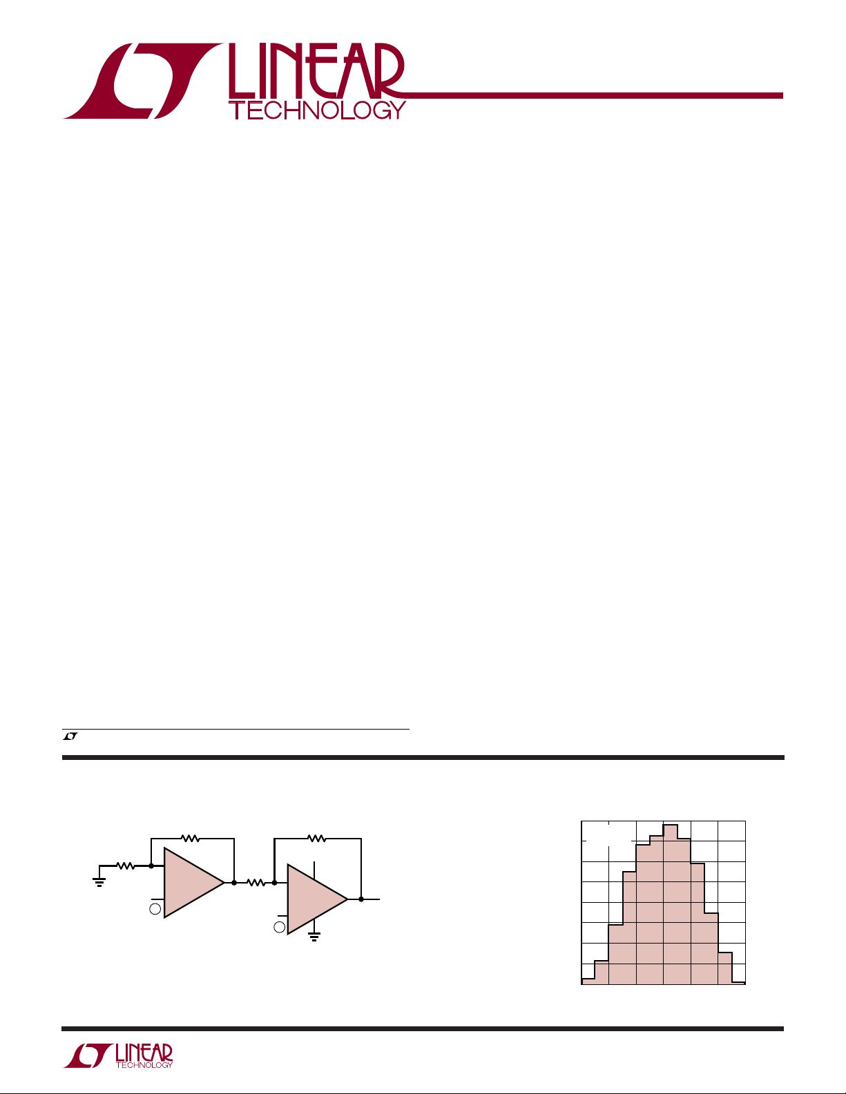
Single Battery, Micropower, Gain = 100, Instrumentation Amplifier
10.1k 1M
10.1k
3V (LITHIUM CELL)
8
–
6
B
7
1/2 LT1078
+
5
4
+
OUTPUT NOISE = 85μV
INPUT RANGE = 0.03V TO 1.8V
OUTPUT RANGE = 0.03V TO 2.3V
OUTPUTS SINK CURRENT—NO PULL-DOWN RESISTORS
ARE NEEDED
OUT
LT1078/79 • TA01
P-P
= 300μV
RMS
(0.3mV ≤ V
0.1Hz TO 10Hz
OVER FULL BANDWIDTH
+
IN
1M
INVERTING
INPUT
TYPICAL PERFORMANCE
INPUT OFFSET VOLTAGE = 40μV
INPUT OFFSET CURRENT = 0.2nA
TOTAL POWER DISSIPATION = 240μW
COMMON MODE REJECTION = 110dB (AMPLIFIER LIMITED)
GAIN BANDWIDTH PRODUCT = 200kHz
2
3
–
–
A
1/2 LT1078
+
1
NONINVERTING
INPUT
– V
–
≤ 23mV)
IN
Distribution of Input Offset Voltage
(LT1078 and LT1079 in H, J, N Packages)
16
VS = 5V, 0V
= 25°C
T
14
A
12
10
8
6
PERCENT OF UNITS
4
2
0
–80 –40 40
–120
INPUT OFFSET VOLTAGE (μV)
0
80
120
1078/79 • TA02
10789fe
1
Page 2
LT1078/LT1079
1
2
3
4
8
7
6
5
TOP VIEW
–IN A
OUT A
V
+
OUT B
+IN A
V
–
+IN B
–IN B
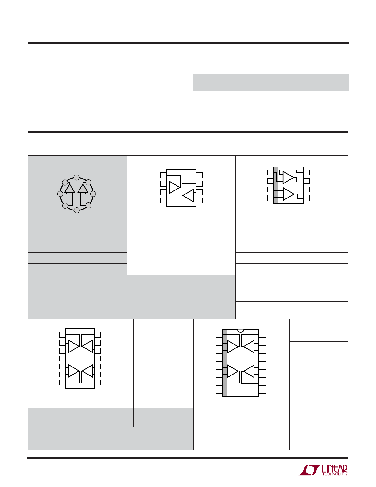
S8 PACKAGE
8-LEAD PLASTIC SO
B
A
NOTE: THIS PIN CONFIGURATION DIFFERS FROM THE
8-LEAD DIP PIN LOCATIONS. INSTEAD, IT FOLLOWS
THE INDUSTRY STANDARD LT1013DS8 SO PACKAGE
CONFIGURATION. FOR SIMILAR PERFORMANCE WITH
TRADITIONAL DIP PINOUT, SEE THE LT2078
WW
W
ABSOLUTE MAXIMUM RATINGS
U
(Note 1)
Supply Voltage ...................................................... ± 22V
Differential Input Voltage ....................................... ± 30V
Input Voltage ............... Equal to Positive Supply Voltage
............5V Below Negative Supply Voltage
Output Short-Circuit Duration .......................... Indefinite
Storage Temperature Range
All Grades ......................................... –65°C to 150°C
U
W
U
PACKAGE/ORDER INFORMATION
TOP VIEW
+
V
8
OUT B
4
–
(CASE)
7
6
–IN B
5
+IN B
OUT A
1
AB
2
–IN A
3
+IN A
V
H PACKAGE
8-LEAD TO-5 METAL CAN
= 150°C, θJA = 150°C/ W, θJC = 45°C/ W
T
JMAX
ORDER PART NUMBER
LT1078ACH
LT1078MH
OBSOLETE PACKAGES
Consider the N8 and S8 Packages for Alternate Source
OUT A
–IN A
+IN A
V
T
JMAX
ORDER PART NUMBER
T
JMAX
TOP VIEW
1
2
A
3
–
4
N8 PACKAGE
8-LEAD PDIP
= 100°C, θJA = 130°C/ W (N8)
LT1078ACN8
LT1078CN8
LT1078IN8
J8 PACKAGE
8-LEAD PDIP
= 150°C, θJA = 100°C/ W (J8)
LT1078AMJ8
LT1078MJ8
Operating Temperature Range
LT1078AM/LT1078M/
LT1079AM/LT1079M (OBSOLETE) ..... –55°C to 125°C
LT1078I/LT1079I .................................... – 40°C to 85°C
LT1078AC/LT1078C/LT1078S8/
LT1079AC/LT1079C .................................... 0°C to 70°C
Lead Temperature (Soldering, 10 sec).................. 300°C
+
8
V
OUT B
7
–IN B
6
B
+IN B
5
T
= 110°C, θJA = 220°C/ W
JMAX
ORDER PART NUMBER
LT1078IS8
LT1078S8
PART MARKING
1078
TOP VIEW
1
OUT A
2
–IN A
+IN A
+IN B
–IN B
OUT B
T
JMAX
T
JMAX
2
A
3
+
4
V
5
6
7
14-LEAD PDIP
= 110°C, θJA = 130°C/ W (N)
14-LEAD CERAMIC DIP
= 150°C, θJA = 100°C/ W (J)
D
B
C
N PACKAGE
J PACKAGE
OBSOLETE PACKAGE
Consider the N Packages for Alternate Source
ORDER PART
14
OUT D
13
–IN D
12
+IN D
–
11
V
10
+IN C
9
–IN C
8
OUT C
NUMBER
LT1079ACN
LT1079CN
LT1079IN
OUT A
–IN A
+IN A
+IN B
–IN B
OUT B
NC
+
V
LT1079MJ
TOP VIEW
1
2
A
3
4
5
B
6
7
8
SW PACKAGE
16-LEAD PLASTIC SO WIDE
NOTE: FOR 14-PIN NARROW
PACKAGE SEE THE LT2079
T
= 110°C, θJA = 150°C/ W
JMAX
D
C
ORDER PART
16
OUT D
15
–IN D
14
+IN D
13
V–
12
+IN C
11
–IN C
10
OUT C
9
NC
NUMBER
LT1079ISW
LT1079SW
10789fe
Page 3
LT1078/LT1079
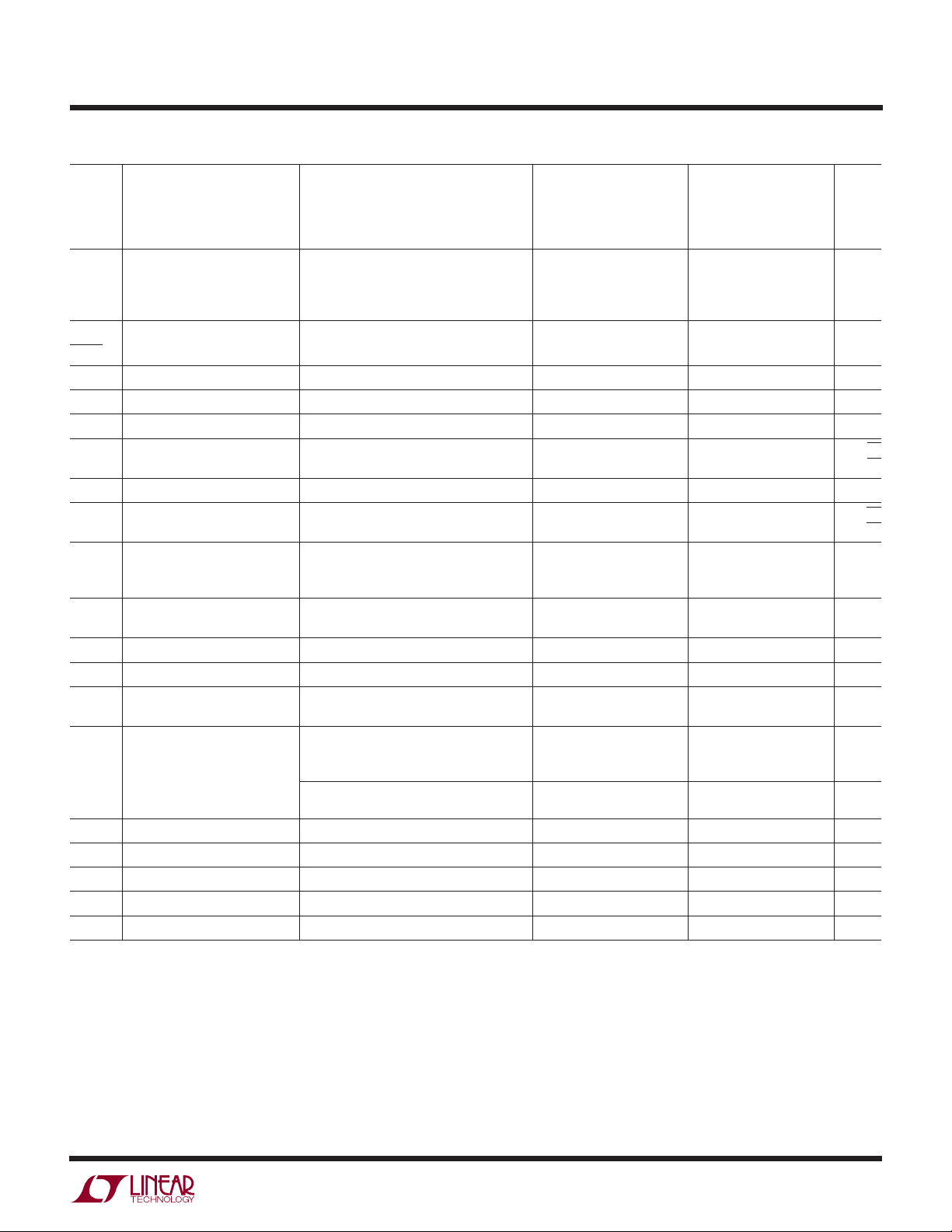
ELECTRICAL CHARACTERISTICS
SYMBOL PARAMETER CONDITIONS (NOTE 2) MIN TYP MAX MIN TYP MAX UNITS
V
OS
ΔV
ΔTime Voltage Stability
I
OS
I
B
e
n
i
n
CMRR Common Mode Rejection Ratio VCM = 0V to 3.5V 97 110 94 108 dB
PSRR Power Supply Rejection Ratio VS = 2.3V to 12V 102 114 100 114 dB
A
VOL
SR Slew Rate AV = 1, VS = ± 2.5V 0.04 0.07 0.04 0.07 V/μs
GBW Gain Bandwidth Product fO ≤ 20kHz 200 200 kHz
I
S
Input Offset Voltage LT1078 30 70 40 120 μV
Long Term Input Offset 0.4 0.5 μV/Mo
OS
Input Offset Current 0.05 0.25 0.05 0.35 nA
Input Bias Current 6 8 6 10 nA
Input Noise Voltage 0.1Hz to 10Hz (Note 3) 0.6 1.2 0.6 μV
Input Noise Voltage Density fO = 10Hz (Note 3) 29 45 29 nV√Hz
Input Noise Current 0.1Hz to 10Hz (Note 3) 2.3 4.0 2.3 pA
Input Noise Current Density fO = 10Hz (Note 3) 0.06 0.10 0.06 pA√Hz
Input Resistance (Note 4)
Differential Mode 400 800 300 800 MΩ
Common Mode 6 6 GΩ
Input Voltage Range 3.5 3.8 3.5 3.8 V
Large-Signal Voltage Gain VO = 0.03V to 4V, No Load 200 1000 150 1000 V/mV
Maximum Output Voltage Output Low, No Load 3.5 6 3.5 6 mV
Swing Output Low, 2k to GND 0.55 1.0 0.55 1.0 mV
Supply Current per Amplifier 38 50 39 55 μA
Channel Separation ΔVIN = 3V, RL = 10k 130 130 dB
Minimum Supply Voltage (Note 5) 2.2 2.3 2.2 2.3 V
LT1078IS8/LT1078S8 60 180 μV
LT1079 35 100 40 150 μV
LT1079ISW/LT1079SW 60 300 μV
fO = 1000Hz (Note 3) 28 37 28 nV√Hz
fO = 1000Hz 0.02 0.02 pA√Hz
VO = 0.03V to 3.5V, RL = 50k 150 600 120 600 V/mV
Output Low, I
Output High, No Load 4.2 4.4 4.2 4.4 V
Output High, 2k to GND 3.5 3.9 3.5 3.9 V
SINK
VS = 5V, 0V, VCM = 0.1V, VO = 1.4V, TA = 25°C unless otherwise noted.
LT1078C/LT1079C
LT1078I/LT1079I
LT1078AC/LT1079AC LT1078M/LT1079M
LT1078AM/LT1079AM LT1078S8/LT1079SW
P-P
P-P
0 – 0.3 0 – 0.3 V
= 100μA 95 130 95 130 mV
10789fe
3
Page 4
LT1078/LT1079
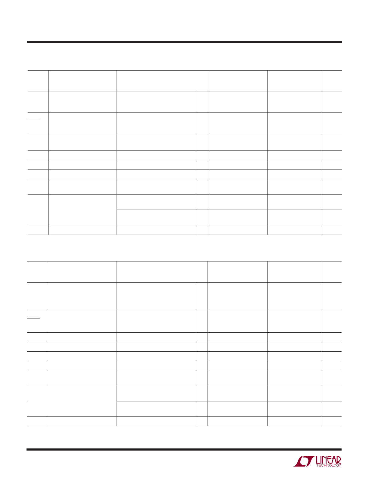
ELECTRICAL CHARACTERISTICS
The ● denotes the specifications which apply over the temperature range
–40°C ≤ TA ≤ 85°C for I grades, – 55°C ≤ TA ≤ 125°C for AM/M grades. VS = 5V, 0V, VCM = 0.1V, VO = 1.4V unless otherwise noted.
SYMBOL PARAMETER CONDITIONS MIN TYP MAX MIN TYP MAX UNITS
V
OS
ΔV
ΔT (Note 6) LT1078IS8
I
OS
I
B
CMRR Common Mode Rejection Ratio VCM = 0.05V to 3.2V ● 92 106 88 104 dB
PSRR Power Supply Rejection Ratio VS = 3.1V to 12V ● 98 110 94 110 dB
A
VOL
I
S
Input Offset Voltage LT1078 ● 70 250 95 370 μV
LT1078IS8/LT1079 ● 80 280 100 400 μV
LT1079ISW ● 100 560 μV
Input Offset Voltage Drift ● 0.4 1.8 0.5 2.5 μV/°C
OS
LT1079ISW ● 0.7 4.0 μV/°C
Input Offset Current ● 0.07 0.50 0.07 0.70 nA
Input Bias Current ● 710 712 nA
Large-Signal Voltage Gain VO = 0.05V to 4V, No Load ● 110 600 80 600 V/mV
Maximum Output Voltage Output Low, No Load
Swing Output Low, I
Supply Current per Amplifier ● 43 60 45 70 μA
LT1078I/LT1079I ● 0.1 1.0 nA
VO = 0.05V to 3.5V, RL = 50k ● 80 400 60 400 V/mV
= 100μA ● 125 170 125 170 mV
SINK
Output High, No Load
Output High, 2k to GND ● 3.0 3.7 3.0 3.7 V
LT1078AM/LT1079AM LT1078M/LT1079M
● 0.6 3.5 μV/°C
● 4.5 8 4.5 8 mV
● 3.9 4.2 3.9 4.2 V
LT1078I/LT1079I
The ● denotes the specifications which apply over the temperature range 0°C ≤ TA ≤ 70°C. VS = 5V, 0V, VCM = 0.1V, VO = 1.4V
unless otherwise noted.
LT1078AC/LT1079AC LT1078S8/LT1079SW
SYMBOL PARAMETER CONDITIONS MIN TYP MAX MIN TYP MAX UNITS
V
OS
ΔV
ΔT (Note 6) LT1078S8
I
OS
I
B
CMRR Common Mode Rejection Ratio VCM = 0V to 3.4V ● 94 108 90 106 dB
PSRR Power Supply Rejection Ratio VS = 2.6V to 12V ● 100 112 97 112 dB
A
VOL
I
S
Input Offset Voltage LT1078 ● 50 150 60 240 μV
Input Offset Voltage Drift ● 0.4 1.8 0.5 2.5 μV/°C
OS
Input Offset Current ● 0.06 0.35 0.06 0.50 nA
Input Bias Current ● 69 611nA
Large-Signal Voltage Gain VO = 0.05V to 4V, No Load ● 150 750 110 750 V/mV
Maximum Output Voltage Output Low, No Load
Swing Output Low, I
Supply Current per Amplifier ● 40 55 42 63 μA
LT1079
LT1078S8
LT1079SW ● 90 480 μV
LT1079SW ● 0.7 4.0 μV/°C
VO = 0.05V to 3.5V, RL = 50k ● 110 500 80 500 V/mV
= 100μA ● 105 150 105 150 mV
SINK
Output High, No Load
Output High, 2k to GND ● 3.3 3.8 3.3 3.8 V
● 60 180 70 270 μV
● 85 350 μV
● 0.6 3.5 μV/°C
● 4.0 7 4.0 7 mV
● 4.1 4.3 4.1 4.3 V
LT1078C/LT1079C
4
10789fe
Page 5
LT1078/LT1079
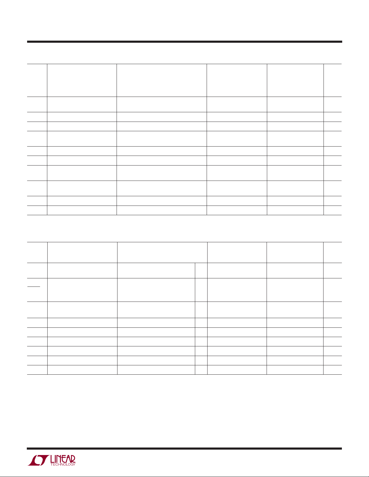
ELECTRICAL CHARACTERISTICS
SYMBOL PARAMETER CONDITIONS MIN TYP MAX MIN TYP MAX UNITS
V
OS
I
OS
I
B
CMRR Common Mode Rejection Ratio VCM = 13.5V, –15V 100 114 97 114 dB
PSRR Power Supply Rejection Ratio VS = 5V, 0V to ±18V 102 114 100 114 dB
A
VOL
V
OUT
SR Slew Rate 0.06 0.10 0.06 0.10 V/μs
I
S
Input Offset Voltage (Including LT1078IS8/LT1078S8) 50 250 70 350 μV
LT1079ISW/LT1079SW 80 500 μV
Input Offset Current 0.05 0.25 0.05 0.35 nA
Input Bias Current 6 8 6 10 nA
Input Voltage Range 13.5 13.8 13.5 13.8 V
Large-Signal Voltage Gain VO = ±10V, RL = 50k 1000 5000 1000 5000 V/mV
VO = ±10V, RL = 2k 400 1100 300 1100 V/mV
Maximum Output Voltage RL = 50k ±13.0 ± 14.0 ±13.0 ± 14.0 V
Swing RL = 2k ±11.0 ± 13.2 ±11.0 ± 13.2 V
Supply Current per Amplifier 46 65 47 75 μA
VS = ± 15V, TA = 25°C unless otherwise noted.
LT1078C/LT1079C
LT1078I/LT1079I
LT1078AC/LT1079AC LT1078M/LT1079M
LT1078AM/LT1079AM LT1078S8/LT1079SW
–15.0 –15.3 –15.0 –15.3 V
The ● denotes the specifications which apply over the temperature range – 40°C ≤ TA ≤ 85°C for I grades, – 55°C ≤ TA ≤ 125°C for
AM/M grades. VS = ± 15V unless otherwise noted.
SYMBOL PARAMETER CONDITIONS MIN TYP MAX MIN TYP MAX UNITS
V
OS
ΔV
ΔT (Note 6) LT1078IS8
I
OS
I
B
A
VOL
CMRR Common Mode Rejection Ratio VCM = 13V, –14.9V ● 94 110 90 110 dB
PSRR Power Supply Rejection Ratio VS = 5V, 0V to ± 18V ● 98 110 94 110 dB
I
S
Input Offset Voltage (Including LT1078IS8) ● 90 430 120 600 μV
LT1079ISW ● 130 825 μV
Input Offset Voltage Drift ● 0.5 1.8 0.6 2.5 μV/°C
OS
LT1079ISW ● 0.8 5.0 μV/°C
Input Offset Current ● 0.07 0.50 0.07 0.70 nA
LT1078I/LT1079I ● 0.1 1.0 nA
Input Bias Current ● 710 712 nA
Large-Signal Voltage Gain VO = ±10V, RL = 5k ● 200 700 150 700 V/mV
Maximum Output Voltage Swing RL = 5k ● ±11.0 ±13.5 ±11.0 ±13.5 V
Supply Current per Amplifier ● 52 80 54 95 μA
LT1078AM/LT1079AM LT1078M/LT1079M
● 0.7 3.8 μV/°C
LT1078I/LT1079I
10789fe
5
Page 6
LT1078/LT1079
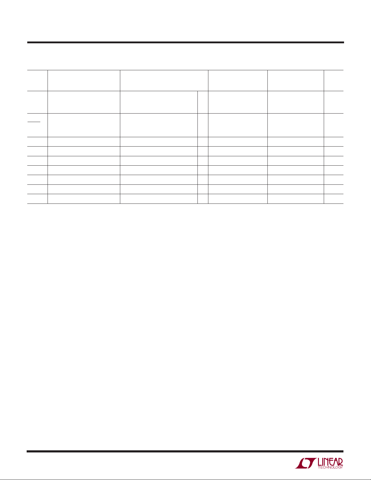
ELECTRICAL CHARACTERISTICS
The ● denotes the specifications which apply over the temperature range
0°C ≤ TA ≤ 70°C. VS = ± 15V unless otherwise noted.
LT1078C/LT1079C
SYMBOL PARAMETER CONDITIONS MIN TYP MAX MIN TYP MAX UNITS
V
OS
ΔV
ΔT (Note 6) LT1078S8
I
OS
I
B
A
VOL
CMRR Common Mode Rejection Ratio VCM = 13V, –15V ● 97 112 94 112 dB
PSRR Power Supply Rejection Ratio VS = 5V, 0V to ± 18V ● 100 112 97 112 dB
I
S
Note 1: Absolute Maximum Ratings are those values beyond which the life
of a device may be impaired.
Note 2: Typical parameters are defined as the 60% yield of parameter
distributions of individual amplifiers, i.e., out of 100 LT1079s (or 100
LT1078s) typically 240 op amps (or 120) will be better than the indicated
specification.
Note 3: This parameter is tested on a sample basis only. All noise
parameters are tested with VS = ±2.5V, VO = 0V.
Input Offset Voltage ● 70 330 90 460 μV
Input Offset Voltage Drift ● 0.5 1.8 0.6 2.5 μV/°C
OS
Input Offset Current ● 0.06 0.35 0.06 0.50 nA
Input Bias Current ● 69 611 nA
Large-Signal Voltage Gain VO = ±10V, RL = 5k ● 300 1200 250 1200 V/mV
Maximum Output Voltage Swing RL = 5k ● ±11.0 ± 13.6 ±11.0 ± 13.6 V
Supply Current per Amplifier ● 49 73 50 85 μA
LT1078S8
LT1079SW ● 115 750 μV
LT1079SW ● 0.8 5.0 μV/°C
Note 4: This parameter is guaranteed by design and is not tested.
Note 5: Power supply rejection ratio is measured at the minimum supply
voltage. The op amps actually work at 1.8V supply but with a typical offset
skew of –300μV.
Note 6: This parameter is not 100% tested.
LT1078AC/LT1079AC LT1078S8/LT1079SW
● 100 540 μV
● 0.7 3.8 μV/°C
6
10789fe
Page 7
W
U
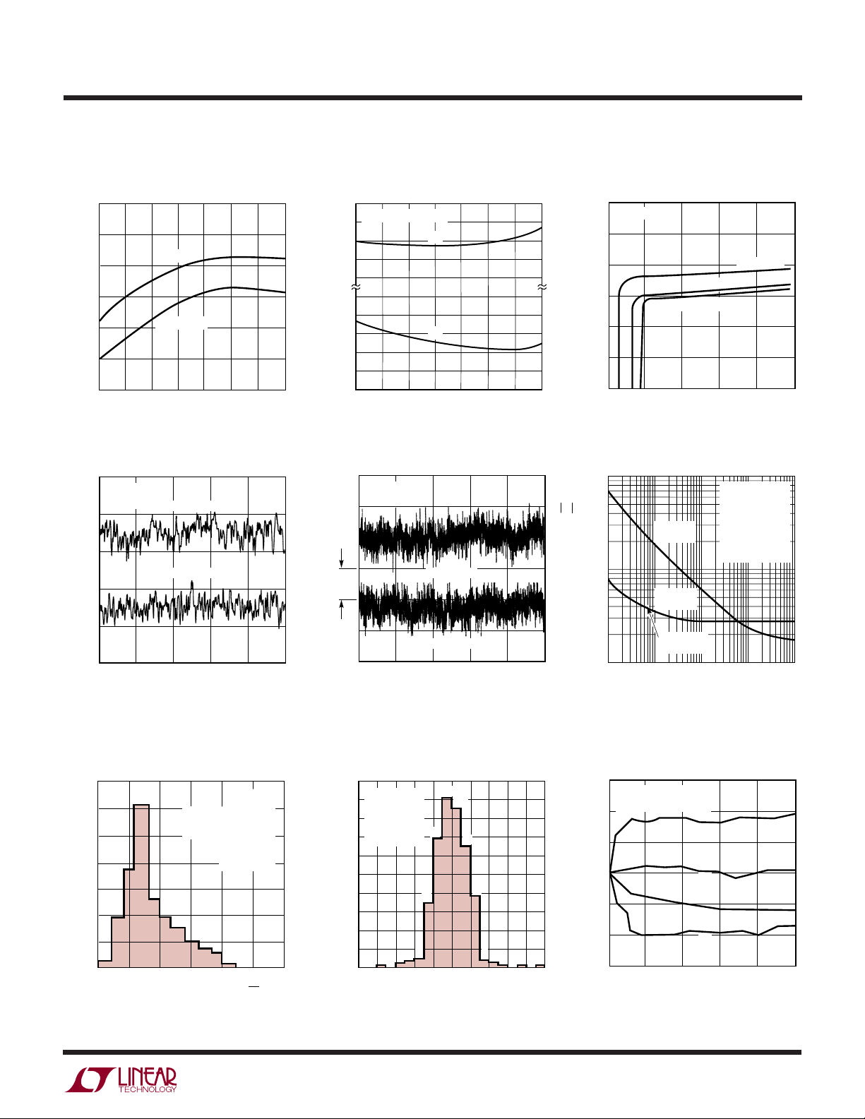
TYPICAL PERFORMANCE CHARACTERISTICS
LT1078/LT1079
Input Bias and Offset Currents
vs TemperatureSupply Current vs Temperature
55
50
–25 0
VS = ±15V
VS = 5V, 0V
50 100 125
25 75
TEMPERATURE (°C)
LT1078/79 • TPC01
45
40
35
30
SUPPLY CURRENT PER AMPLIFIER (μA)
25
–50
100
VS = 5V, 0V TO ±15V
50
0
–5
–6
–7
BIAS CURRENT (nA) OFFSET CURRENT (pA)
–50
0
–25
TEMPERATURE (°C)
I
OS
I
B
50
25
75
100
LT1078/79 • TPC02
125
Input Bias Current
vs Common Mode Voltage
0
VS = 5V, 0V
–2
–4
–6
–8
INPUT BIAS CURRENT (nA)
–10
–12
–1
0.1Hz to 10Hz Noise 0.01Hz to 10Hz Noise Noise Spectrum
1000
300
100
30
CURRENT NOISE DENSITY (fA/√Hz)
VOLTAGE NOISE DENSITY (nV/√Hz)
10
0.1 1 100
NOISE VOLTAGE (0.4μV/DIV)
TA = 25°C
V
0
= ±2.5V
S
TA = 25°C
= ±2.5V
V
0.4μV
S
CHANNEL A
CHANNEL B
20
0
40
TIME (SEC)
60
80
100
LT1078/79 • TPC05
CHANNEL A
CHANNEL B
NOISE VOLTAGE (0.4μV/DIV)
2
4
TIME (SEC)
6
8
10
LT1078/79 • TPC04
TA = –55°C
TA = 25°C
TA = 125°C
0123
COMMON MODE VOLTAGE (V)
LT1078/79 • TPC03
TA = 25°C
= ±2.5V
V
S
= ±15V
(AT V
S
CURRENT
NOISE
VOLTAGE
NOISE
1/f CORNER
0.7Hz
FREQUENCY (Hz)
VOLTAGE NOISE
IS 4% LESS
CURRENT NOISE
IS UNCHANGED)
10 1000
LT1078/79 • TPC06
4
10Hz Voltage Noise Distribution
35
30
25
20
15
PERCENT OF UNITS
10
5
0
25
VOLTAGE NOISE DENSITY (nV/√Hz)
329 OP AMPS TESTED
FROM THREE RUNS
30
TA = 25°C
= ± 2.5V
V
S
106 LT1078'S
45 LT1079'S
35 40
LT1078/79 • TPC07
Distribution of Offset Voltage Drift
with Temperature (In All Packages
Except Surface Mount)
25
VS = 5V, 0V
= 0.1V
V
CM
120 LT1078'S
20
70 LT1079'S
520 OP AMPS
15
10
PERCENT OF UNITS
5
1111
0
–2 –1 0 1 2
OFFSET VOLTAGE DRIFT WITH TEMPERATURE (μV/°C)
120
109
89
85
44
7
5
3
47
4
3
LT1078/79 • TPC08
Long Term Stability of Two
Representative Units (LT1078)
15
TA = 25°C, VS = 5V, 0V
= 0.1V
V
CM
10
5
0
–5
OFFSET VOLTAGE CHANGE (μV)
–10
–15
0
1234
1A
2B
1B
2A
TIME (MONTHS)
5
LT078/79 • TPC09
10789fe
7
Page 8
LT1078/LT1079
W
U
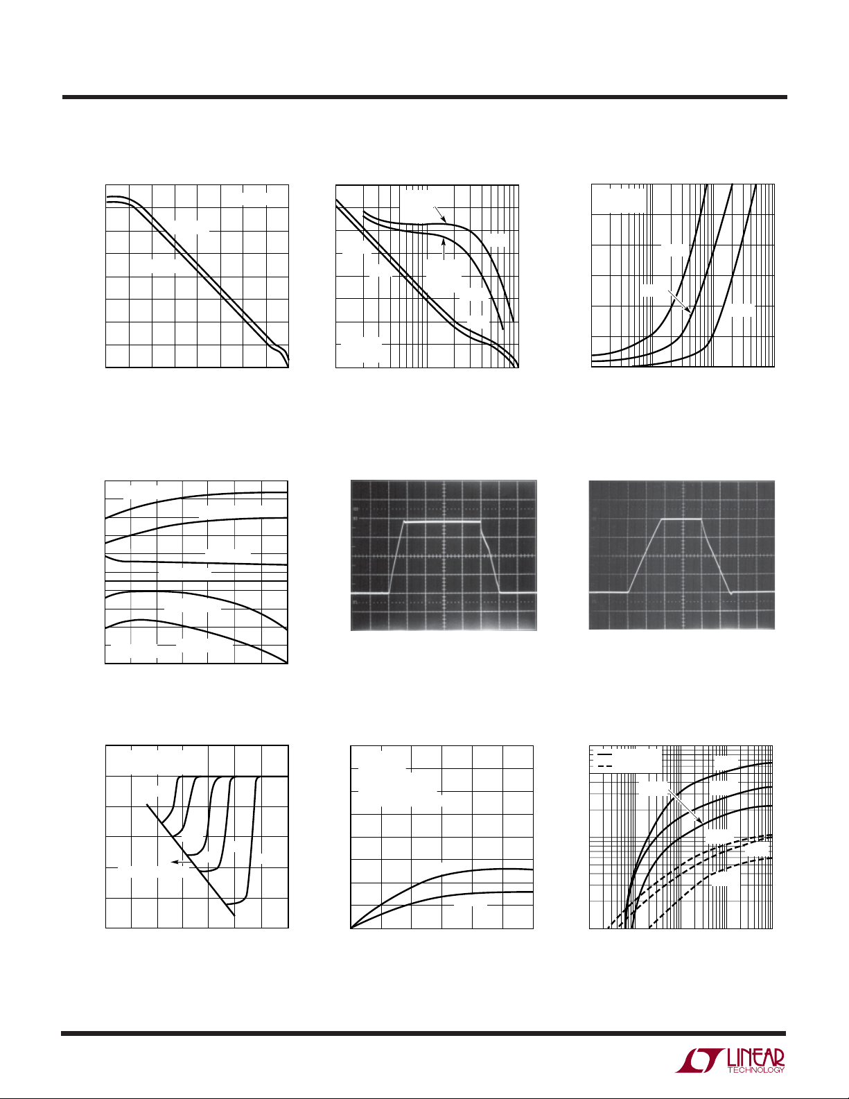
TYPICAL PERFORMANCE CHARACTERISTICS
Voltage Gain vs Frequency
140
120
100
80
60
40
VOLTAGE GAIN (dB)
20
0
–20
0.01
0.1
VS = ±15V
VS = 5V, 0V
1
10
FREQUENCY (Hz)
Slew Rate, Gain Bandwidth
Product and Phase Margin vs
Temperature
0.12
0.10
0.08
0.06
0.04
PRODUCT (kHz) SLEW RATE (V/μs)
GAIN BANDWIDTH
240
220
200
180
160
fO = 20kHz
–50
SLEW = ±15V
φM = 5V, 0V
0
–25
TEMPERATURE (°C)
GBW = ±15V
GBW = 5V, 0V
25
100
1k
SLEW = 5V, 0V
φM = ±15V
50
TA = 25°C
10k
LT1078/79 • TPC10
75
LT1078/79 • TPC13
100k
100
30
20
10
VOLTAGE GAIN (dB)
0
–10
1M
PHASE MARGIN (DEG)
80
70
60
50
40
125
Gain, Phase vs Frequency
PHASE
MARGIN
66°
5V, 0V
TA = 25°C
C
L
10
GAIN
= 20pF
30
FREQUENCY (kHz)
PHASE
MARGIN
54°
100
±15V
5V, 0V
±15V
300
LTC1078/79 TPC11
Large-Signal Transient Response
VS = 5V, 0V
1V/DIV
AV = 1, NO LOAD 50μs/DIV
INPUT PULSE 0V TO 3.8V
100
120
140
160
180
200
1000
LT1078/79 • TPC27
Capacitive Load Handling
120
TA = 25°C
V
S
100
PHASE SHIFT (DEG)
80
60
OVERSHOOT (%)
40
20
0
10
Large-Signal Transient Response
VS = ± 15V
5V/DIV
0V
AV = 1 100μs/DIV
NO LOAD
= 5V, 0V
AV = 5
CAPACITIVE LOAD (pF)
AV = 1
1000100
AV = 10
10000
LT1078/79 • TPC12
0V
LT1078/79 • TPC28
8
Minimum Supply Voltage
100
–100
–200
–300
INPUT OFFSET VOLTAGE (μV)
–400
–500
V– = 0V
–0.1V ≤ V
0
NONFUNCTIONAL
0
≤ 0.4V
CM
125°C
1
POSITIVE SUPPLY VOLTAGE (V)
70°C
0°C
25°C
23
–55°C
LT1078/79 • TPC16
Warm-Up Drift
0.8
TA = 25°C
V
0.7
S
WARM UP DRIFT
AT V
0.6
IMMEASURABLY LOW
0.5
0.4
0.3
0.2
CHANGE IN OFFSET VOLTAGE (μV)
0.1
0
0
= ±15V
= 5V, 0V IS
S
LT1079
LT1078
12
TIME AFTER POWER-ON (MINUTES)
LT1078/79 • TPC17
10M
VOLTAGE GAIN (V/V)
100k
3
Voltage Gain vs Load Resistance
VS = ±15V
= 5V, 0V
V
S
125°C
1M
100
LOAD RESISTANCE TO GROUND (Ω)
10k 100k1k 1M
25°C
–55°C
–55°C
125°C
25°C
LT1078/79 • TPC18
10789fe
Page 9
W
U
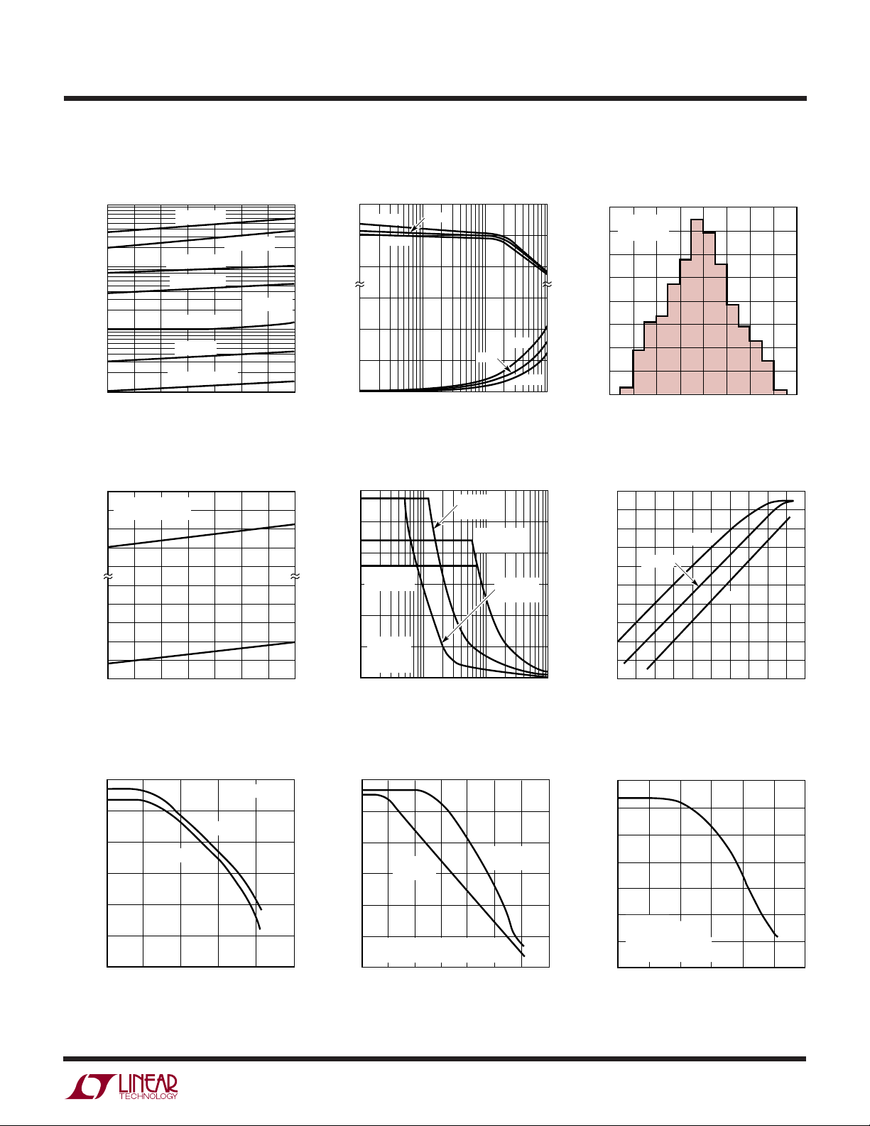
TYPICAL PERFORMANCE CHARACTERISTICS
LT1078/LT1079
Output Saturation vs Temperature
vs Sink Current
1000
100
10
SATURATION VOLTAGE (mV)
1
–25 125
–50
I
= 2mA
SINK
I
SINK
I
= 100μA
SINK
I
= 10μA
SINK
I
= 1μA
SINK
NO LOAD
RL = 5k TO GND
0 25 50 10075
TEMPERATURE (°C)
= 1mA
VS = 5V, 0V
LT1078/79 • TPC19
Common Mode Range
vs Temperature Closed Loop Output Impedance
+
V
V+ = 2.5V TO 18V
–
= 0V TO –18V
V
V+ – 1
+
V
– 2
–
V
+ 1
–
COMMON MODE RANGE (V)
V
–
V
– 1
–25 0 25 50 75
–50
TEMPERATURE (°C)
100
LT1078/79 • TPC22
125
Output Voltage Swing
vs Load Current
+
V
125°C
V+ – 1
+
– 2
V
–
V
+ 2
OUTPUT VOLTAGE SWING (V)
–
+ 1
V
–
V
0.01
SOURCING OR SINKING LOAD CURRENT (mA)
25°C
–55°C
0.1 1
Undistorted Output Swing
vs Frequency
30
= ±15V (V)
S
20
VS = 5V, 0V
≥ 1k
R
L
10
TA = 25°C
,
LOAD R
L
TO GND
PEAK-TO-PEAK OUTPUT SWING, V
0
0.01
VS = ±15V
R
110
FREQUENCY (kHz)
25°C
≥ 100k
L
VS = 5V, 0V
R
L
125°C
LT1078/79 • TPC20
≥ 100k
VS = ±15V
= 30k
R
L
LT1078/79 • TPC23
–55°C
Distribution of Input Offset Voltage
(LT1078 in 8-Pin SO Package)
16
TA = 25°C
14
= 5V, 0V
V
S
12
10
8
6
PERCENT OF UNITS
4
2
10
100
5
4
3
2
1
0
0
–160
–120
PEAK-TO-PEAK OUTPUT SWING, V
1k
100
10
S
1
= 5V, 0V (V)
OUTPUT IMPEDANCE (Ω)
0.1
10 100 1k 10k 100k
–80
INPUT OFFSET VOLTAGE (μV)
A
= 10
V
0
–40
AV = 100
FREQUENCY (Hz)
40
AV = 1
80
120
LT1078/79 • TPC21
LT1078/79 • TPC24
160
Common Mode Rejection Ratio
vs Frequency
120
100
VS = ±15V
80
60
40
20
COMMON MODE REJECTION RATIO (dB)
0
10
VS = 5V, 0V
100 1k 10k 100k
FREQUENCY (Hz)
TA = 25°C
LT1078/79 • TPC25
1M
Power Supply Rejection Ratio
vs Frequency
120
100
80
NEGATIVE
0.1
TA = 25°C
V
S
SUPPLY
= ±2.5V + 1V
110
FREQUENCY (Hz)
SINE WAVE
P-P
1k 100k 1M
100 10k
60
40
20
POWER SUPPLY REJECTION RATIO (dB)
0
POSITIVE
SUPPLY
LT1078/79 • TPC26
Channel Separation vs Frequency
140
120
100
80
60
40
TA = 25°C
CHANNEL SEPARATION (dB)
= ±2.5V
V
S
20
= 3V
IN
= 10k
L
10 100
TO 2kHz
P-P
FREQUENCY (Hz)
10k 1M
V
R
0
1 1k 100k
LT1078/79 • TPC27
10789fe
9
Page 10
LT1078/LT1079
W
U
TYPICAL PERFORMANCE CHARACTERISTICS
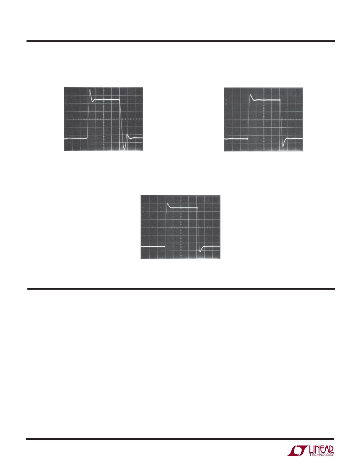
Small-Signal Transient Response
V
= 5V, 0V
S
20mV/DIV
AV = 1 10μs/DIV
= 15pF
C
L
INPUT 50mV TO 150mV
LT1078/79 • TPC24
0.1V
Small-Signal Transient Response
VS = ± 15V
20mV/DIV
Small-Signal Transient Response
V
= ± 2.5V
S
20mV/DIV
AV = 1 10μs/DIV
= 15pF
C
L
0V
LT1078/79 • TPC25
0V
AV = 1 10μs/DIV
= 15pF
C
L
U
WUU
APPLICATIONS INFORMATION
The LT1078/LT1079 devices are fully specified with
V+ = 5V, V– = 0V, VCM = 0.1V. This set of operating
conditions appears to be the most representative for
battery-powered micropower circuits. Offset voltage is
internally trimmed to a minimum value at these supply
voltages. When 9V or 3V batteries or ± 2.5V dual supplies
are used, bias and offset current changes will be minimal.
Offset voltage changes will be just a few microvolts as
given by the PSRR and CMRR specifications. For example,
if PSRR = 114dB (= 2μV/V), at 9V the offset voltage change
will be 8μV. Similarly, VS = ± 2.5V, VCM = 0V is equivalent
to a common mode voltage change of 2.4V or a V
change of 7μV if CMRR = 110dB (3μV/V).
OS
LT1078/79 • TPC26
A full set of specifications is also provided at ± 15V supply
voltages for comparison with other devices and for completeness.
Single Supply Operation
The LT1078/LT1079 are fully specified for single supply
operation, i.e., when the negative supply is 0V. Input
common mode range goes below ground and the output
swings within a few millivolts of ground while sinking
current. All competing micropower op amps either cannot
swing to within 600mV of ground (OP-20, OP-220, OP-420)
or need a pull-down resistor connected to the output to swing
to ground (OP-90, OP-290, OP-490, HA5141/42/44). This
10
10789fe
Page 11
LT1078/LT1079
U
WUU
APPLICATIONS INFORMATION
difference is critical because in many applications these
competing devices cannot be operated as micropower op
amps and swing to ground simultaneously.
As an example, consider the instrumentation amplifier
shown on the front page. When the common mode signal
is low and the output is high, amplifier A has to sink
current. When the common mode signal is high and the
output low, amplifier B has to sink current. The competing
devices require a 12k pull-down resistor at the output of
amplifier A and a 15k at the output of B to handle the
specified signals. (The LT1078 does not need pull-down
resistors.) When the common mode input is high and the
output is high these pull-down resistors draw 300μA (150μA
each), which is excessive for micropower applications.
The instrumentation amplifier is by no means the only
application requiring current sinking capability. In seven
of the nine single supply applications shown in this data
sheet the op amps have to be able to sink current. In two
of the applications the first amplifier has to sink only the
6nA input bias current of the second op amp. The competing devices, however, cannot even sink 6nA without a pulldown resistor
enough to make the amplifier function properly in the
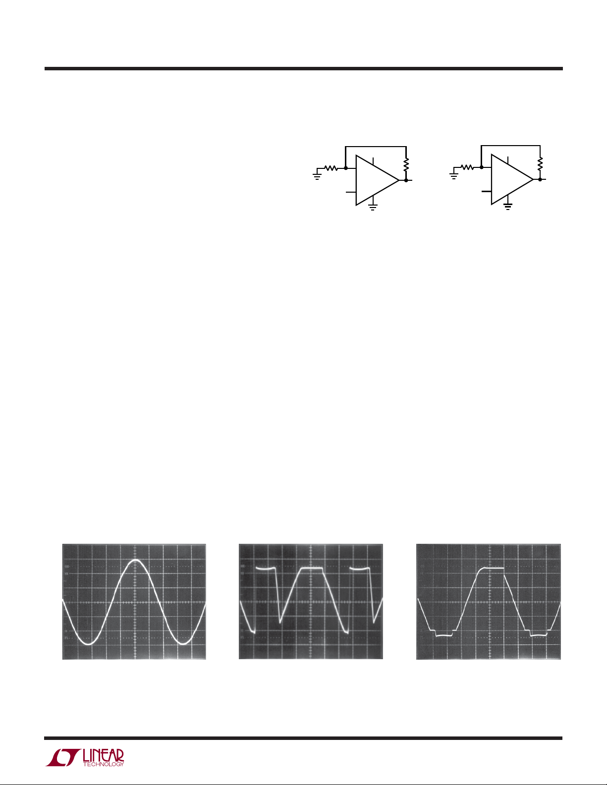
voltage follower mode, Figure 1b.
R
1mV
Figure 1a. Gain 100 Amplifier
5V
–
+
99R
100mV
LT1078/79 • F01a
R
1mV
Figure 1b. Voltage Follower
5V
–
+
99R
100mV
LT1078/79 • F01a
Single supply operation can also create difficulties at the
input. The driving signal can fall below 0V — inadvertently
or on a transient basis. If the input is more than a few
hundred millivolts below ground, two distinct problems
can occur on previous single supply designs, such as the
LM124, LM158, OP-20, OP-21, OP-220, OP-221, OP-420
(1 and 2), OP-90/290/490 (2 only):
1. When the input is more than a diode drop below ground,
unlimited current will flow from the substrate (V
–
terminal) to the input. This can destroy the unit. On the
LT1078/LT1079, resistors in series with the input protect
the devices even when the input is 5V below ground.
Since the output of the LT1078/LT1079 cannot go exactly
to ground, but can only approach ground to within a few
millivolts, care should be exercised to ensure that the
output is not saturated. For example, a 1mV input signal
will cause the amplifier to set up in its linear region in the
gain 100 configuration shown in Figure 1a, but is not
4V
2V
0V
6V
INPUT 1ms/DIV
P-P
–1V TO 5V
LT1078/79 • F02a
Figure 2. Voltage Follower with Input Exceeding the Negative Common Mode Range (VS = 5V, 0V)
4V
2V
0V
OP-90 EXHIBITS OUTPUT PHASE REVERSAL
2. When the input is more than 400mV below ground (at
25°C), the input stage saturates and phase reversal
occurs at the output. This can cause lockup in servo
systems. Due to a unique phase reversal protection circuitry, the LT1078/LT1079 output does not reverse, as
illustrated in Figure 2, even when the inputs are at –1V.
4V
2V
0V
1ms/DIV
LT1078/79 • F02b
LT1078/LT1079 NO PHASE REVERSAL
1ms/DIV
LT1078/79 • F02C
10789fe
11
Page 12
LT1078/LT1079
U
WUU
APPLICATIONS INFORMATION
Matching Specifications
In many applications the performance of a system depends on the matching between two op amps, rather than
the individual characteristics of the two devices. The two
and three op amp instrumentation amplifier configurations shown in this data sheet are examples. Matching
characteristics are not 100% tested on the LT1078/LT1079.
Table 1
LT1078AC/LT1079AC/LT1078AM/LT1079AM LT1078C/LT1079C/LT1078M/LT1079M
PARAMETER 50% YIELD 98% YIELD 50% YIELD 98% YIELD UNITS
VOS Match, ΔV
Temperature Coefficient ΔV
Average Noninverting I
Match of Noninverting I
CMRR Match 120 100 117 97 dB
PSRR Match 117 105 117 102 dB
OS
LT1078 30 110 50 190 μV
LT1079 40 150 50 250 μV
OS
B
B
0.5 1.2 0.6 1.8 μV/°C
68610 nA
0.12 0.4 0.15 0.5 nA
Some specifications are guaranteed by definition. For
example, 70μV maximum offset voltage implies that mis-
match cannot be more than 140μV. 97dB (= 14μV/V)
CMRR means that worst-case CMRR match is 91dB
(= 28μV/V). However, Table 1 can be used to estimate the
expected matching performance at V
= 5V, 0V between
S
the two sides of the LT1078, and between amplifiers A and
D, and between amplifiers B and C of the LT1079.
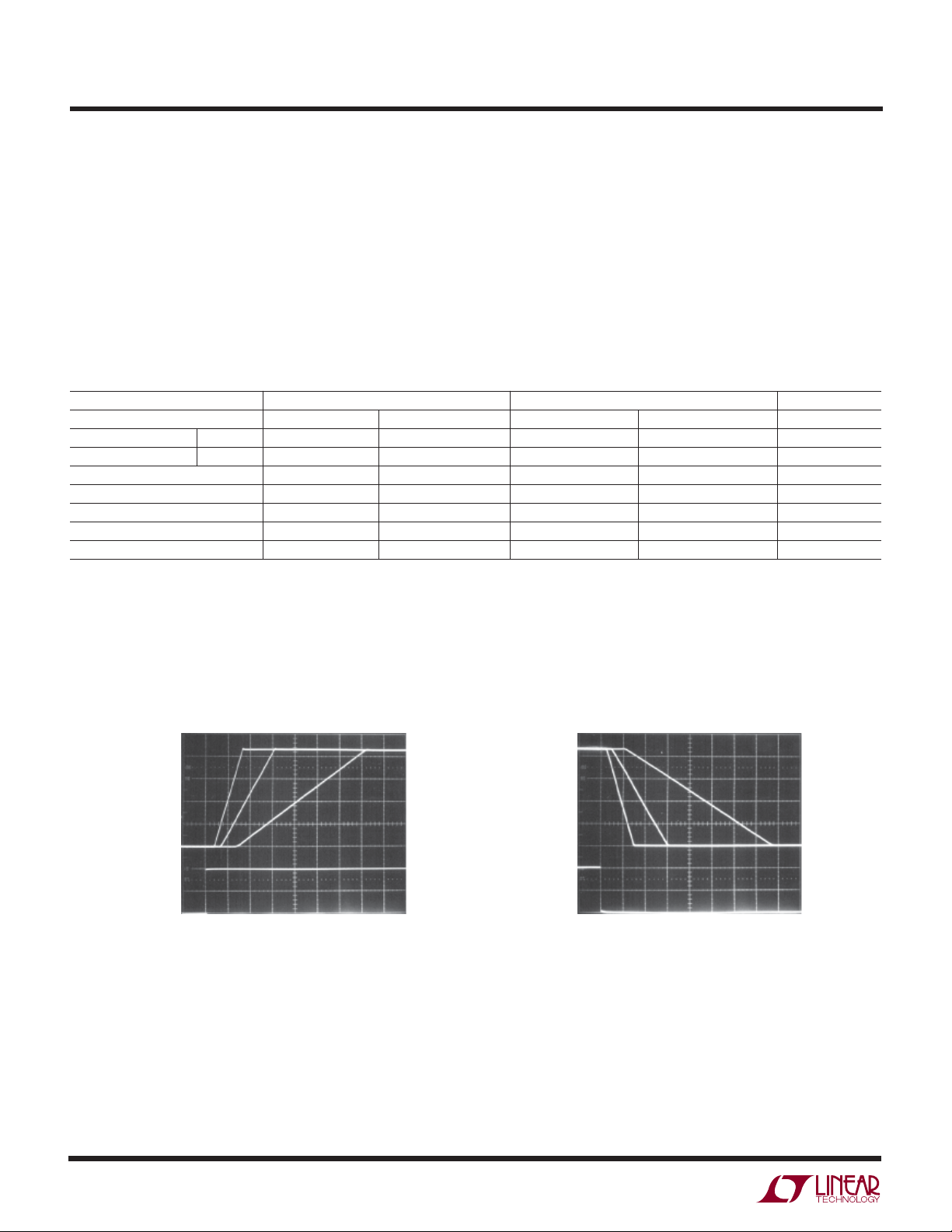
Comparator Applications
The single supply operation of the LT1078/LT1079 and its
ability to swing close to ground while sinking current
4
2
0
0
–100
INPUT (mV) OUTPUT (V)
= 5V, 0V 200μs/DIV
V
S
Figure 3. Comparator Rise Response
Time to 10mV, 5mV, 2mV Overdrives
LT2078/79 • F03
lends itself to use as a precision comparator with TTL
compatible output.
4
2
0
100
0
INPUT (mV) OUTPUT (V)
VS = 5V, 0V 200μs/DIV
Figure 4. Comparator Fall Response
Time to 10mV, 5mV, 2mV Overdrives
LT2078/79 • F04
12
10789fe
Page 13
U
TYPICAL APPLICATIONS
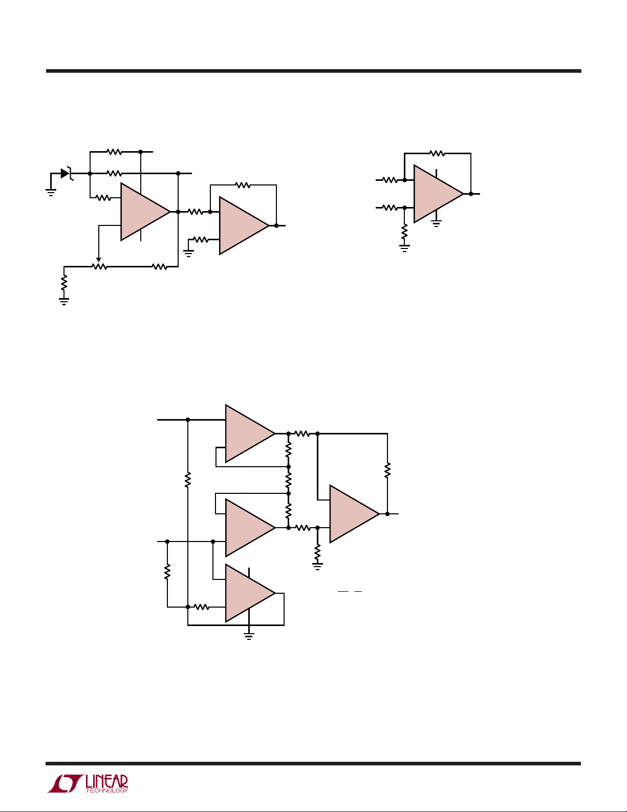
Micropower, 10ppm/°C, ±5V Reference Gain of 10 Difference Amplifier
2M
LT1034BC-1.2
160k
1%
THE LT1078 CONTRIBUTES LESS THAN 3% OF THE TOTAL OUTPUT NOISE AND
DRIFT WITH TIME AND TEMPERATURE. THE ACCURACY OF THE –5V OUTPUT
DEPENDS ON THE MATCHING OF THE TWO 1M RESISTORS
220k
120k
3
2
20k
SUPPLY CURRENT = 9V BATTERY = 115μA
OUTPUT NOISE = 36μV
9V
8
+
1/2 LT1078
–
4
–9V
510k
1%
–9V BATTERY = 85μA
P-P
5.000V
1M
1
510k
, 0.1Hz TO 10Hz
OUT
6
–
1/2 LT1078
5
+
1M
7
–5.000V
LT1078/79 • TA03
OUT
LT1078/LT1079
10M
1M
–IN
1M
+IN
BANDWIDTH= 20kHz
OUTPUT OFFSET= 0.7mV
OUTPUT NOISE= 80μV
THE USEFULNESS OF DIFFERENCE AMPLIFIERS IS LIMITED BY
THE FACT THAT THE INPUT RESISTANCE IS EQUAL TO THE SOURCE
RESISTANCE. THE PICOAMPERE OFFSET CURRENT AND LOW
CURRENT NOISE OF THE LT1078 ALLOWS THE USE OF 1M SOURCE
RESISTORS WITHOUT DEGRADATION IN PERFORMANCE. IN ADDITION,
WITH MEGOHM RESISTORS MICROPOWER OPERATION CAN BE MAINTAINED
–
1/2 LT1078
+
10M
3V
(0.1Hz TO 10Hz)
P-P
260μV
RMS
BANDWIDTH
OUTPUT
0.0035V TO 2.4V
OVER FULL
LT1078/79 • TA04
Picoampere Input Current, Triple Op Amp Instrumentation Amplifier with Bias Current Cancellation
–IN
+IN
R
10M
2R
20M
2R
20M
3
2
6
5
12
13
+
1/4 LT1079
–
–
1/4 LT1079
+
9V
4
+
1/4 LT1079
–
11
R2
1M
1
R1
1M
R3
R
G
200k
9
R1
1M
7
R2
1M
14
–
1/4 LT1079
10
+
R3
9.1M
2R1
GAIN = 1 +
INPUT BIAS CURRENT TYPICALLY < 150pA
INPUT RESISTANCE = 3R = 30M FOR VALUES SHOWN
NEGATIVE COMMON MODE LIMIT = (I
GAIN BANDWIDTH PRODUCT = 1.8MHz
R3
()
R
R2
G
9.1M
8
OUTPUT
4mV TO 8.2V
LT`1078/79 • TA05
= 100 FOR VALUES SHOWN
)(2R) + 20mV ≈ 140mV
B
10789fe
13
Page 14
LT1078/LT1079
TYPICAL APPLICATIONS
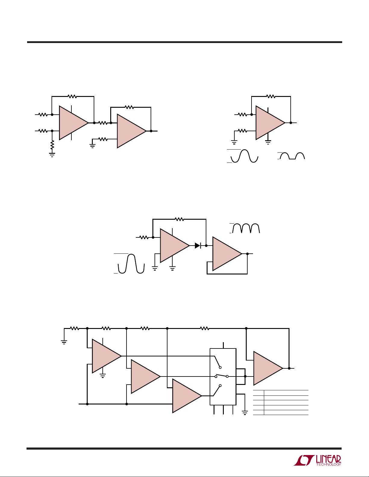
85V, –100V Common Mode Range
Instrumentation Amplifier (A
1M
V
U
= 10)
Half-Wave Rectifier
2M
+IN
–IN
10M
2
–
10M
1/2 LT1078
3
+
1M
BANDWIDTH= 2kHz
OUTPUT OFFSET= 8mV
OUTPUT NOISE= 0.8mV
INPUT RESISTANCE = 10M
9V
–9V
10M
8
100k
1
4
= 1.4mV
(DOMINATED BY RESISTOR NOISE)
6
–
100k
1/2 LT1078
5
+
(0.1Hz TO 10Hz)
P-P
OVER FULL BANDWIDTH
RMS
7
OUTPUT
8V TO –9V
LT1078/79 • TA06
1.8V
–1.8V
INPUT
2M
1M
3V
–
1/2 LT1078
+
1.8V
OUTPUT
V
= 6mV
OMIN
NO DISTORTION TO 100Hz
0V
LT1078/79 • TA07
Absolute Value Circuit (Full-Wave Rectifier)
200k
5
+
1/2 LT1078
6
–
= 4mV
3.5V
0V
7
LT1078/79 • TA08
OUTPUT
3.5V
–3.5V
INPUT
200k
2
–
1/2 LT1078
3
+
5V
8
1
1N4148
4
V
OMIN
NO DISTORTION TO 100Hz
14
Programmable Gain Amplifier (Single Supply)
3V TO 18V
4
2
–
1/4 LT1079
3
+
IN
ERROR DUE TO SWITCH ON RESISTANCE,
LEAKAGE CURRENT, NOISE AND TRANSIENTS
ARE ELIMINATED
1
6
11
–
1/4 LT1079
5
+
7
9
10
–
1/4 LT1079
+
1M100k10k1.11k
1
3
88
3V TO 18V
A
B
C
CD4016B
13 5 6
11
13
–
2
4
9
7
1/4 LT1079
12
+
GAIN PIN 13 PIN 5 PIN 6
1000 HIGH LOW LOW
100 LOW HIGH LOW
10 LOW LOW HIGH
14
LT1078/79 • TA09
CD4016B
OUT
10789fe
Page 15

U
TYPICAL APPLICATIONS
Single Supply, Micropower, Second Order Lowpass Filter with 60Hz Notch
LT1078/LT1079
0.02μF
27.6k
0.1%
IN
Y INPUT
(5mV TO 50V)
X INPUT
(5mV TO 50V)
505k
0.1%
505k
0.1%
27.6k
0.1%
f
= 40Hz
C
Q > 30
0.01μF
9V
–
6
1/4 LT1079
+
5
–1.5V TO – 9V
–
2
1/4 LT1079
+
3
1000pF
0.5%
6
–
1/2 LT1078
5
+
7
LT1078/79 • TA10
5V
8
3
+
1/2 LT1078
2
–
4
5.1M1%120k
100pF
5%
2.64M
0.1%
1
1000pF
0.5%
2.64M
0.1%
2000pF
0.5%
1.35M
0.1%
Micropower Multiplier/Divider
220pF 220pF
4
714
11
220pF
1
Q1
30k
5%
Q2 Q4
30k
5%
Q3
30k
5%
499k
0.5%
10
–
9
1/4 LT1079
+
1/4 LT1079
10k
GAIN
–
+
8
13
12
OUTPUT
(5mV TO 8V)
OUTPUT
TYPICAL OFFSET
≈ 600μV
505k
0.1%
Z INPUT
(5mV TO 50V)
LT1078/79 • TA11
Q1,Q2, Q3, Q4 = MAT-04
TYPICAL LINEARITY = 0.01% OF FULL-SCALE OUTPUT
OUTPUT = , POSITIVE INPUTS ONLY
NEGATIVE SUPPLY CURRENT = 165μA +
POSITIVE SUPPLY CURRENT = 165μA +
BANDWIDTH (< 3V
(X)(Y)
(Z)
SIGNAL): X AND Y INPUTS = 10kHz
P-P
Z INPUT = 4kHz
X + Y+ Z + OUT
500k
OUT
500k
10789fe
15
Page 16
LT1078/LT1079
TYPICAL APPLICATIONS
U
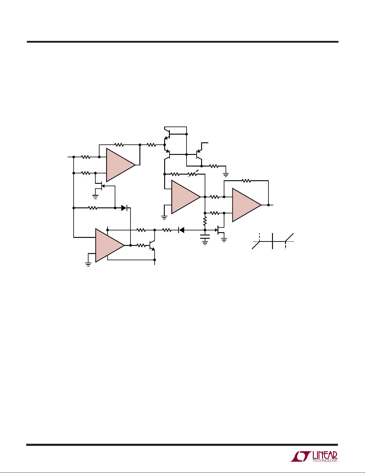
Micropower Dead Zone Generator
INPUT
1M**
510k
Q1
2N4393
1M
6
5
–
2
+
3
9V
–
1/4 LT1079
+
1M**
1/4 LT1079
1N914
4
11
1
1M 680k
1M
7
Q4
1M*
Q2 Q3
1M*
–
9
1/4 LT1079
+
10
1N914
Q5
BIPOLAR SYMMETRY IS EXCELLENT
BECAUSE ONE DEVICE, Q2,
SETS BOTH LIMITS
SUPPLY CURRENT ≈ 240μA
–9V
BANDWIDTH = 150kHz
GAIN
200k
1000pF
V
SET
DEAD ZONE
CONTROL INPUT
0.4V TO 5V
470k
1M**
8
510k
510k
1M**
–
13
14
V
LT1078/79 • TA12
V
OUT
OUT
V
SET
1/4 LT1079
+
12
Q6
2N4393
1% FILM
*
RATIO MATCH 0.05%
**
Q2, Q3, Q4, Q5 CA3096 TRANSISTOR ARRAY
V
SET
V
IN
16
10789fe
Page 17

U
TYPICAL APPLICATIONS
Lead-Acid Low-Battery Detector with System Shutdown
2M1%2M
255k1%280k
1%
1%
910k
5%
3
+
1/2 LT1078
2
–
LT1004-1.2
TOTAL SUPPLY CURRENT = 105μA
5
+
1/2 LT1078
6
–
LT1078/79 • TA13
1
8
4
BATTERY
OUTPUT
12V
LO = BATTERY LOW
< 10.90V)
(IF V
S
LO = SYSTEM SHUTDOWN
7
(IF V
< 10.05V)
S
LT1078/LT1079
LT1004-1.2
Platinum RTD Signal Conditioner with Curvature Correction
3V (LITHIUM)
8
1
1/2 LT1078
4
= ROSEMOUNT 118MF
R
P
**
= TRW MAR-6 0.1%
*
= 1% METAL FILM
13k*
10k*
50k
5°C
TRIM
12.3k*
1k**
1k**
R
1k AT
0°C
1k**
P
1μF
3
+
2
–
1μF
220°C
43.2k**
–
6
1/2 LT1078
+
5
1.21M*
(SELECT AT 110°C)
5k
TRIM
0.02V TO 2.2V
7
2°C TO 220°C ±0.1°C
LT1078/79 • TA14
OUT
=
10789fe
17
Page 18
LT1078/LT1079
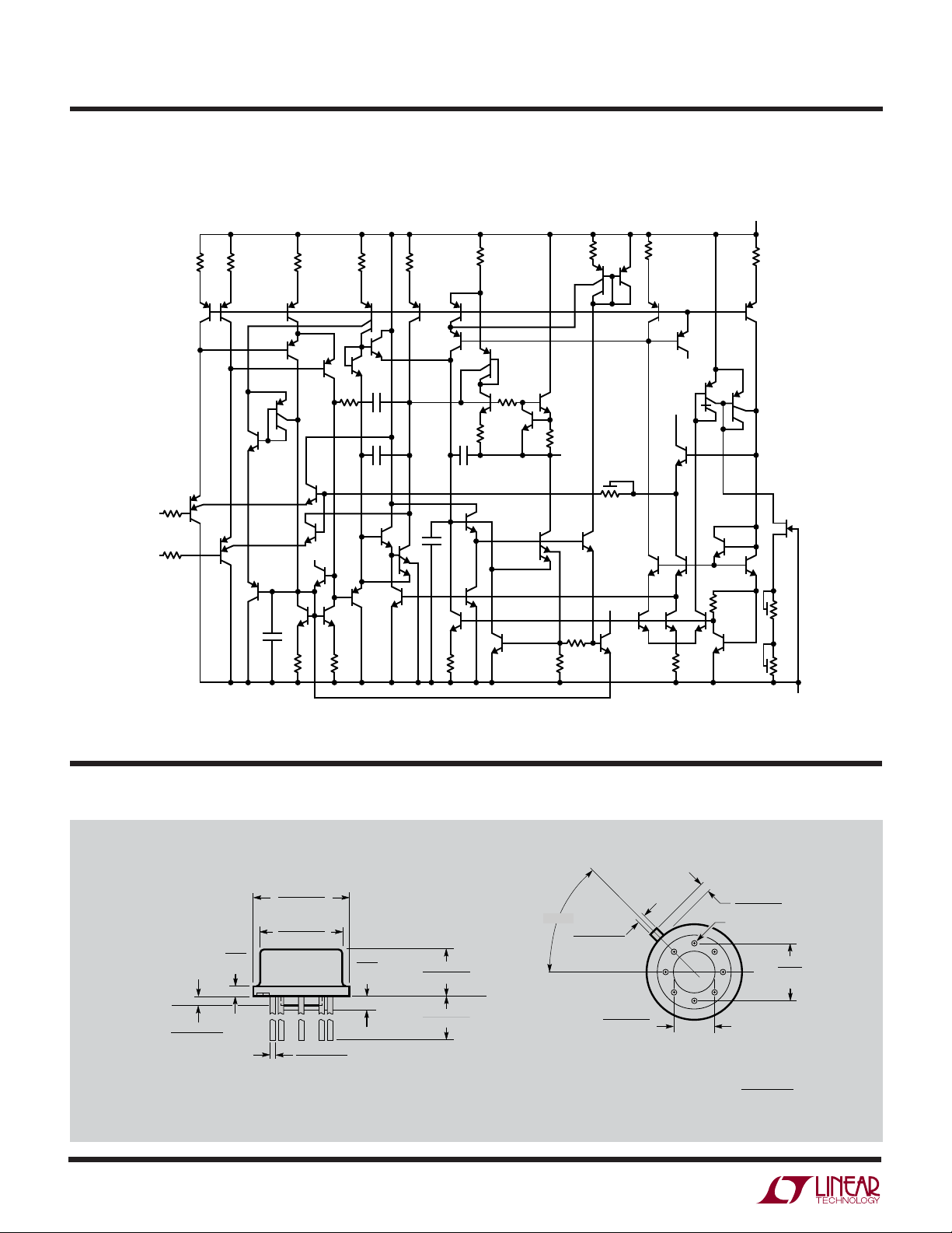
SI PLIFIED
SCHEMATIC
WW
1/2 LT1078, 1/4 LT1079
+
V
11.5k
Q53
2
Q47
Q46
–
V
+
V
Q44
Q48
Q42
Q50
+
V
Q38
Q45
Q55
Q51
Q43
5.35k
Q40
Q41
9.1k
LT1078/79 • SIMPLIFIED SCHEM
Q49
Q52
12.5k
J1
700k
700k
–
V
Q36
30Ω
OUT
30Ω
5k
Q54
1
1
150k
Q33
10k
1
C4
4pF
1.35k
Q25
Q30
3.6k
3
3k
Q35
Q26
2.9k
Q31
Q23
Q34
10k 10k 2.2k 5.6k
C2
Q16 Q14
Q3
Q12
4
1
Q39
Q7
6.2k
Q27
V
+
Q28
Q24
Q4
8.6k
50pF
2.5pF
Q10
Q8
6.2k
Q6
Q5
Q11
Q1
600Ω
–
IN
+
IN
600Ω
Q21
Q2
Q22
Q9
175pF
Q29
C1
C5
Q18
Q17
1.3k
Q15 Q32
C3
40pF
Q19
Q37
Q20
PACKAGE DESCRIPTIO
0.335 – 0.370
(8.509 – 9.398)
DIA
0.305 – 0.335
(7.747 – 8.509)
0.016 – 0.021**
(0.406 – 0.533)
SEATING
PLANE
0.010 – 0.045*
(0.254 – 1.143)
0.040
(1.016)
MAX
18
U
H Package
8-Lead TO-5 Metal Can (.230 Inch PCD)
(Reference LTC DWG # 05-08-1321)
45°TYP
0.028 – 0.034
(0.711 – 0.864)
0.050
(1.270)
MAX
0.165 – 0.185
GAUGE
PLANE
(4.191 – 4.699)
0.500 – 0.750
(12.700 – 19.050)
REFERENCE
PLANE
OBSOLETE PACKAGE
*
LEAD DIAMETER IS UNCONTROLLED BETWEEN THE REFERENCE PLANE
AND 0.045" BELOW THE REFERENCE PLANE
**
FOR SOLDER DIP LEAD FINISH, LEAD DIAMETER IS
0.110 – 0.160
(2.794 – 4.064)
INSULATING
STANDOFF
0.027 – 0.045
(0.686 – 1.143)
PIN 1
0.016 – 0.024
(0.406 – 0.610)
H8 (TO-5) 0.230 PCD 1197
0.230
(5.842)
TYP
10789fe
Page 19
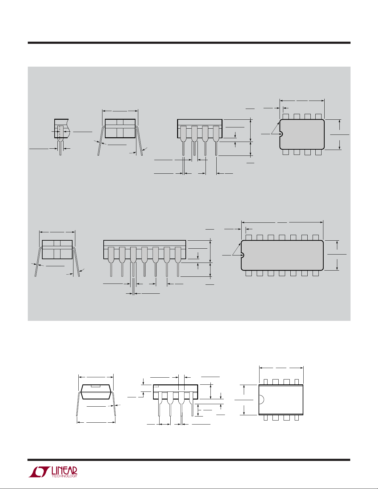
PACKAGE DESCRIPTIO
CORNER LEADS OPTION
(4 PLCS)
0.023 – 0.045
(0.584 – 1.143)
HALF LEAD
0.045 – 0.068
(1.143 – 1.727)
FULL LEAD
OPTION
0.300 BSC
(0.762 BSC)
0.008 – 0.018
(0.203 – 0.457)
NOTE: LEAD DIMENSIONS APPLY TO SOLDER DIP/PLATE
OR TIN PLATE LEADS
OPTION
NOTE: LEAD DIMENSIONS APPLY TO SOLDER DIP/PLATE
OR TIN PLATE LEADS
0° – 15°
0.300 BSC
(0.762 BSC)
0.008 – 0.018
(0.203 – 0.457)
0.045 – 0.065
(1.143 – 1.651)
U
J8 Package
8-Lead CERDIP (Narrow .300 Inch, Hermetic)
(Reference LTC DWG # 05-08-1110)
(5.080)
0.015 – 0.060
(0.381 – 1.524)
0° – 15°
0.045 – 0.065
(1.143 – 1.651)
0.014 – 0.026
(0.360 – 0.660)
J Package
14-Lead CERDIP (Narrow .300 Inch, Hermetic)
(Reference LTC DWG # 05-08-1110)
0.200
(5.080)
MAX
0.015 – 0.060
(0.381 – 1.524)
0.014 – 0.026
(0.360 – 0.660)
0.100
(2.54)
BSC
0.125
(3.175)
MIN
0.100
(2.54)
BSC
0.005
(0.127)
MIN
0.025
(0.635)
RAD TYP
0.200
MAX
0.025
(0.635)
RAD TYP
0.125
3.175
MIN
14
234
1
LT1078/LT1079
0.405
87
12
0.785
MAX
11 891013
(10.287)
MAX
65
3
56
4
7
0.005
(0.127)
MIN
(19.939)
12
0.220 – 0.310
(5.588 – 7.874)
J8 1298
0.220 – 0.310
(5.588 – 7.874)
J14 1298
OBSOLETE PACKAGES
N8 Package
8-Lead PDIP (Narrow .300 Inch)
(Reference LTC DWG # 05-08-1510)
0.300 – 0.325
(7.620 – 8.255)
0.065
(1.651)
0.009 – 0.015
(0.229 – 0.381)
+0.035
0.325
–0.015
+0.889
8.255
()
–0.381
*THESE DIMENSIONS DO NOT INCLUDE MOLD FLASH OR PROTRUSIONS.
MOLD FLASH OR PROTRUSIONS SHALL NOT EXCEED 0.010 INCH (0.254mm)
TYP
Information furnished by Linear Technology Corporation is believed to be accurate and reliable.
However, no responsibility is assumed for its use. Linear Technology Corporation makes no representation that the interconnection of its circuits as described herein will not infringe on existing patent rights.
0.045 – 0.065
(1.143 – 1.651)
0.100
(2.54)
BSC
0.130 ± 0.005
(3.302 ± 0.127)
0.125
(3.175)
MIN
0.018 ± 0.003
(0.457 ± 0.076)
0.020
(0.508)
MIN
0.255 ± 0.015*
(6.477 ± 0.381)
0.400*
(10.160)
MAX
87 6
1234
5
N8 1098
10789fe
19
Page 20
LT1078/LT1079
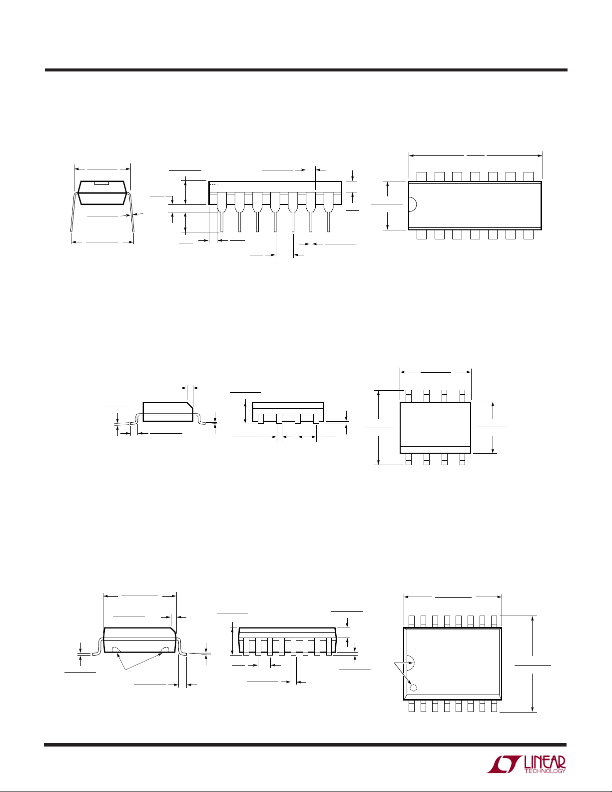
PACKAGE DESCRIPTION
0.300 – 0.325
(7.620 – 8.255)
0.009 – 0.015
(0.229 – 0.381)
+0.035
0.325
–0.015
+0.889
8.255
()
–0.381
*THESE DIMENSIONS DO NOT INCLUDE MOLD FLASH OR PROTRUSIONS.
MOLD FLASH OR PROTRUSIONS SHALL NOT EXCEED 0.010 INCH (0.254mm)
0.010 – 0.020
(0.254 – 0.508)
0.008 – 0.010
(0.203 – 0.254)
*
DIMENSION DOES NOT INCLUDE MOLD FLASH. MOLD FLASH
SHALL NOT EXCEED 0.006" (0.152mm) PER SIDE
**
DIMENSION DOES NOT INCLUDE INTERLEAD FLASH. INTERLEAD
FLASH SHALL NOT EXCEED 0.010" (0.254mm) PER SIDE
0.130 ± 0.005
(3.302 ± 0.127)
0.020
(0.508)
MIN
× 45°
0.016 – 0.050
(0.406 – 1.270)
0.125
(3.175)
MIN
8-Lead Plastic Small Outline (Narrow .150 Inch)
0°– 8° TYP
U
N Package
14-Lead PDIP (Narrow .300 Inch)
(Reference LTC DWG # 05-08-1510)
0.045 – 0.065
(1.143 – 1.651)
0.005
(0.125)
MIN
0.100
(2.54)
BSC
S8 Package
(Reference LTC DWG # 05-08-1610)
0.053 – 0.069
(1.346 – 1.752)
0.014 – 0.019
(0.355 – 0.483)
TYP
0.018 ± 0.003
(0.457 ± 0.076)
0.004 – 0.010
(0.101 – 0.254)
0.050
(1.270)
BSC
0.065
(1.651)
TYP
0.255 ± 0.015*
(6.477 ± 0.381)
0.228 – 0.244
(5.791 – 6.197)
14
0.189 – 0.197*
(4.801 – 5.004)
8
1
0.770*
(19.558)
MAX
11
1213
31
2
7
2
5
6
3
4
5
4
0.150 – 0.157**
(3.810 – 3.988)
SO8 1298
8910
7
6
N14 1098
SW Package
16-Lead Plastic Small Outline (Wide .300 Inch)
0.291 – 0.299**
(7.391 – 7.595)
0° – 8° TYP
0.093 – 0.104
(2.362 – 2.642)
0.010 – 0.029
(0.254 – 0.737)
0.009 – 0.013
(0.229 – 0.330)
NOTE:
1. PIN 1 IDENT, NOTCH ON TOP AND CAVITIES ON THE BOTTOM OF PACKAGES ARE THE MANUFACTURING OPTIONS.
THE PART MAY BE SUPPLIED WITH OR WITHOUT ANY OF THE OPTIONS
DIMENSION DOES NOT INCLUDE MOLD FLASH. MOLD FLASH SHALL NOT EXCEED 0.006" (0.152mm) PER SIDE
*
DIMENSION DOES NOT INCLUDE INTERLEAD FLASH. INTERLEAD FLASH SHALL NOT EXCEED 0.010" (0.254mm) PER SIDE
**
NOTE 1
× 45°
0.016 – 0.050
(0.406 – 1.270)
(Reference LTC DWG # 05-08-1620)
0.050
(1.270)
BSC
0.014 – 0.019
(0.356 – 0.482)
TYP
Linear Technology Corporation
20
1630 McCarthy Blvd., Milpitas, CA 95035-7417
(408) 432-1900 ● FAX: (408) 434-0507
●
www.linear.com
0.037 – 0.045
(0.940 – 1.143)
0.004 – 0.012
(0.102 – 0.305)
NOTE 1
0.398 – 0.413*
(10.109 – 10.490)
15 1413121110 9
16
2345
1
LT/CPI 1201 1.5K REV E • PRINTED IN USA
© LINEAR TECHNOLOGY CORPORATION 1994
6
78
0.394 – 0.419
(10.007 – 10.643)
S16 (WIDE) 1098
10789fe
 Loading...