

Page 1
FEATURES
LT1032
Quad Low Power
Line Driver
U
DESCRIPTIO
■
Low Operating Voltage: ±5V to ±15V
■
500µA Supply Current
■
Zero Supply Current when Shut Down
■
Outputs Can Be Driven ±30V
■
Thermal Limiting
■
Output “Open” when Off (Three-State)
■
10mA Output Drive
■
Pinout Similar to 1488
U
APPLICATIO S
■
RS232
■
Power Supply Inverter
■
Micropower Interface
■
Level Translator
The LT®1032 is a RS232 and RS423 line driver that
operates over a ±5V to ±15V range on low supply current
and can be shut down to zero supply current. Outputs are
fully protected from externally applied voltages of ±30V by
both current and thermal limiting. Since the output swings
to within 200mV of the positive supply and 600mV of the
negative supply, power supply needs are minimized.
Also included is a strobe pin to force all outputs low
independent of input or shutdown conditions. Further,
slew rate can be adjusted with a resistor connected to the
supply.
A major advantage of the LT1032 is the high impedance
output state when off or powered down.
For applications requiring dual or triple RS232 driver/
receiver devices, see the LT1180A (dual), LT1039A (triple)
or the LT1130A data sheets.
, LTC and LT are registered trademarks of Linear Technology Corporation.
TYPICAL APPLICATIO
RS232 Line Driver
1
–6V
INPUT
OUTPUT
ON/OFF
(0V TO 5V)
†
INPUT
OUTPUT
GND
*NO CONNECTION NEEDED WHEN NOT USED
†
5V = ON
LT1032
2
3
4
5
6
7
U
14
6V
13
STROBE*
12
INPUT
11
OUTPUT
10
RESPONSE TIME
CONTROL*
9
INPUT
8
OUTPUT
LT1032 • TA01
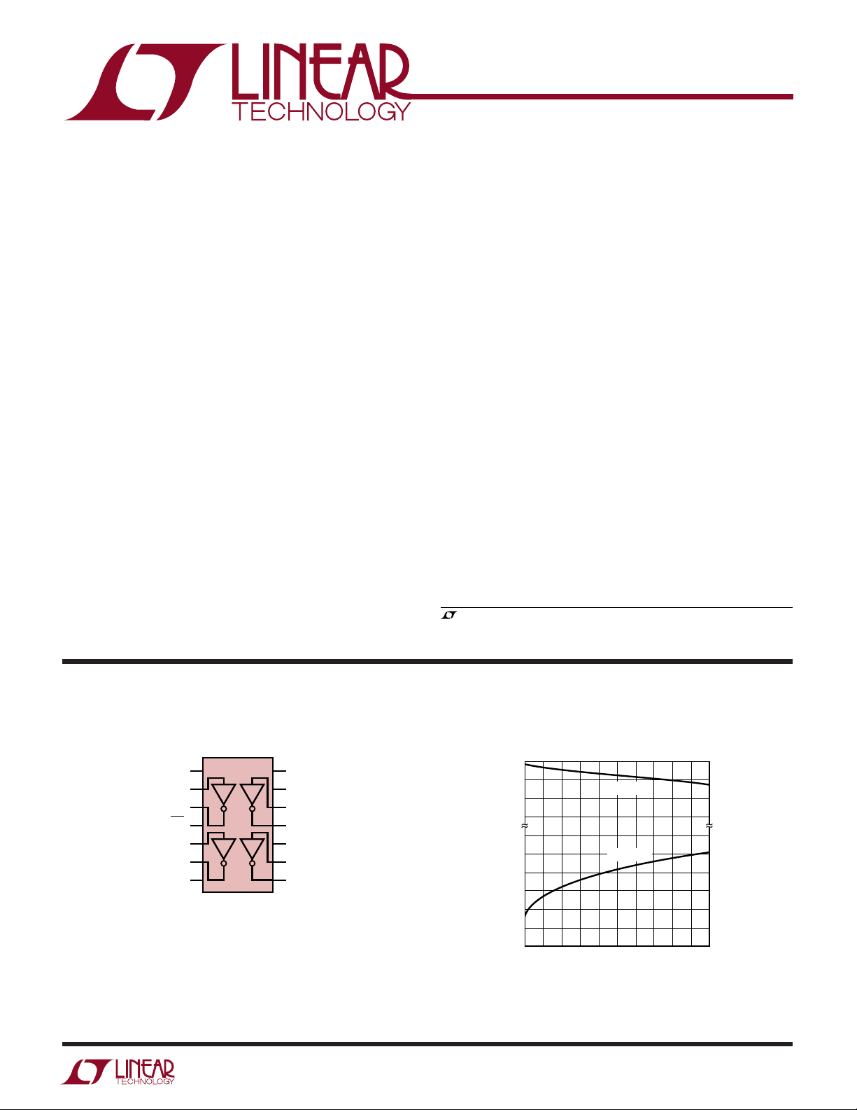
Output Swing vs Output Current
+
V
0.2
0.4
1.0
0.8
0.6
0.4
0.2
–
OUTPUT VOLTAGE REFERRED TO SUPPLIES (V)
V
2
0
V
HIGH
OUT
V
LOW
OUT
6
4
OUTPUT CURRENT (mA)
8
10
LT1032 • TA02
1
Page 2
LT1032
TOP VIEW
SW PACKAGE
16-LEAD PLASTIC SO (WIDE)
1
2
3
4
5
6
7
8
16
15
14
13
12
11
10
9
V
EE
ON/OFF
GND
NC
V
CC
STROBE
NC
RESPONSE
CONTROL
A
W
O
LUTEXI TIS
S
A
WUW
U
(Note 1)
ARB
G
Supply Voltage ..................................................... ±15V
Logic Input Pins ............................................ V– to 25V
ON/OFF Pin ................................................. GND to 15V
Output (Forced) ............................. V– + 30V, V+ – 30V
Response Pin ......................................................... ±6V
Short-Circuit Duration (to ±30V) .................... Indefinite
Storage Temperature Range ................ –65°C to 150°C
WU
/
1
2
3
4
5
6
7
O
RDER I FOR ATIO
TOP VIEW
V
CC
14
(5V TO 15V)
STROBE
13
12
11
RESPONSE
10
CONTROL
9
8
N PACKAGE
14-LEAD PDIP
ORDER PART
NUMBER
LT1032CJ
LT1032CN
LT1032IN
LT1032MJ
PACKAGE
V
EE
(–15V TO – 5V)
ON/OFF
(0V TO 5V)
GND
J PACKAGE
14-LEAD CERDIP
T
= 85°C, θJA = 100°C/W, θJC = 60°C (CJ)
JMAX
= 85°C, θJA = 100°C/W, θJC = 60°C (CN)
T
JMAX
= 150°C, θJA = 100°C/W, θJC = 60°C (MJ)
T
JMAX
Operating Temperature Range
LT1032C............................................... 0°C to 70°C
LT1032I........................................... – 40°C to 85°C
LT1032M....................................... – 55°C to 125°C
C Grade Guaranteed
Functional by Design .............................. –25°C to 85°C
Lead Temperature (Soldering, 10 sec)................. 300°C
U
ORDER PART
NUMBER
LT1032CSW
LT1032ISW
T
= 85°C, θJA = 80°C/W
JMAX
LECTRICAL C CHARA TERIST
E
The ● denotes specifications which apply over the full operating temperature
ICS
range, otherwise specifications are at TA = 25°C. Supply voltage = ±5V to ±15V
PARAMETER CONDITIONS MIN TYP MAX UNITS
Supply Current V
Power Supply Leakage Current V
Output Voltage Swing Load = 2mA Positive V+ – 0.3V V+ – 0.1V V
Output Current (Active) V
Output Current (Shutdown) V
Output Overload Voltage (Forced) Operating or Shutdown ● V+ – 30V V– + 30V V
Input Overload Voltage (Forced) Operating of Shutdown ● V
Logic Input Levels Low Input (V
Logic Input Current VIN > 2.0V 2 20 µA
ON/OFF Pin Current 0 ≤ VIN ≤ 5V ● –10 3 50 µA
Slew Rate I
Change in Slew Rate (Note 3) I
Response Pin Leakage V
Note 1: Absolute Maximum Ratings are those values beyond which the life
of a device may be impaired.
Note 2: 3V applied to the strobe pin will force all outputs low. Strobe pin
input impedance is about 2k to ground. Leave open when not used.
2
≥ 2.4V, I
ON/OFF
≤ 0.4V 1 10 µA
ON/OFF
≤ 0.1V, TA = 125°C ● 10 50 µA
V
ON/OFF
= ±5V to ±15V 10 22 mA
SUPPLY
= 0V, V
SUPPLY
V
= ±15V, V
SUPPLY
High Input (V
V
< 0.8V 10 20 µA
IN
RESPONSE
RESPONSE
I
RESPONSE
V
= 0, RL = 3k 4 15 30 V/µs
= 50µA 50 %
= –50µA–50%
= ±6V, V
SUPPLY
RESPONSE
= ±6V
= 0, All Outputs Low ● 500 1000 µA
OUT
Negative V
= ±30V 2 100 µA
OUT
= ±20V 2 100 µA
OUT
–
= High) ● 1.4 0.8 V
OUT
= Low) ● 2 1.4 V
OUT
≤ 0.4V 1 µA
ON/OFF
Note 3: Response can be changed by connecting a resistor to the supply.
For supplies less than ±6V this current is disconnected when shut down.
Leave open when not used.
–
+ 0.7V V– + 0.9V V
30V V
Page 3
LPER
F
O
R
ATYPICA
UW
CCHARA TERIST
E
C
LT1032
ICS
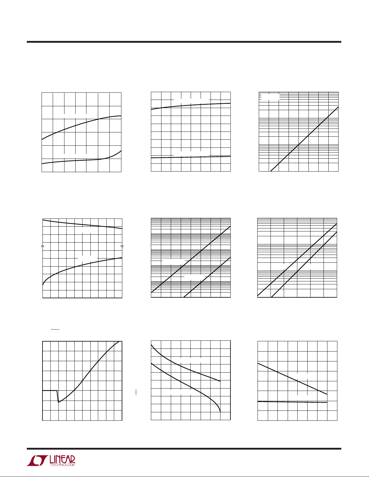
On Supply Current
vs Temperature
3.0
2.5
2.0
1.5
1.0
SUPPLY CURRENT (mA)
0.5
0
–50
ALL OUTPUTS HIGH
ALL OUTPUTS LOW
–25 0
50 100 125
25 75
TEMPERATURE (˚C)
LT1032 • TPC01
Output Swing vs Output Current
+
V
0.2
0.4
1.0
0.8
0.6
0.4
0.2
–
OUTPUT VOLTAGE REFERRED TO SUPPLIES (V)
V
2
0
V
HIGH
OUT
V
LOW
OUT
6
4
OUTPUT CURRENT (mA)
8
LT1032 • TA02
10
Supply Current
vs Supply Voltage
2.0
1.8
1.6
1.4
1.2
1.0
0.8
0.6
SUPPLY CURRENT (mA)
0.4
0.2
0
5
ALL OUTPUTS HIGH
ALL OUTPUTS LOW
7.5
10
SUPPLY VOLTAGE (±V)
Output Leakage vs Temperature
100µA
10µA
1µA
V
= –30V
100nA
OUTPUT CURRENT
10nA
1nA
OUT
V
= 30V
OUT
25 75 100
50
TEMPERATURE (°C)
12.5
LT1032 • TPC02
LT1032 • TPC05
125
Off Supply Current
vs Temperature
1000
VS = ±12V
100
10
SUPPLY CURRENT (nA)
1
15
25
50 100 125
75
TEMPERATURE (°C)
LT1032 • TPC03
Response Pin Leakage
vs Temperature (Device Off)
1000
100
10
RESPONSE PIN LEAKAGE (µA)
1
25
V = 5V V = –5V
50 75 100
TEMPERATURE (°C)
LT1032 • G06
ON/OFF Pin Current vs Voltage
10
8
6
4
2
0
CURRENT (µA)
–2
–4
–6
1
0
INPUT VOLTAGE (V)
3
2
4
LT1032 • TPC07
Shutdown Pin Voltage
vs Temperature
2.0
1.8
1.6
1.4
1.2
1.0
0.8
0.6
ON/OFF PIN VOLTAGE (V)
0.4
0.2
0
–50
5
–25 25
MIN ON VOLTAGE
MAX OFF VOLTAGE
0
50
TEMPERATURE (°C)
125
100
75
150
LT1032 • TPC08
Current Limit vs Temperature
80
70
60
50
40
30
OUTPUT CURRENT (mA)
20
10
0
–25
–55
SINKING
SOURCING
0
50
25
TEMPERATURE (°C)
75
100
125
LT1032 • TPC09
150
3
Page 4

LT1032
LPER
F
O
R
ATYPICA
UW
CCHARA TERIST
E
C
ICS
Output Swing vs Temperature
+
V
200
400
1
800
600
400
200
–
OUTPUT VOLTAGE REFERRED TO SUPPLIES (V)
V
–50
–25 25
0
TEMPERATURE (°C)
ON/OFF Response Time
6V
4V
V
OUT
V
OUT
ON/OFF
INPUT
2V
0
0
–2V
–4V
–6V
5V
0
0 200µs 400µs
VIN = 0V
VIN = 5V
Slew Rate vs Temperature
20
I
= 2mA
OUT
I
= 10mA
OUT
I
= –10mA
OUT
I
= –2mA
OUT
125
50
100
75
150
LT1032 • TPC10
18
16
14
12
10
8
SLEW RATE (V/µs)
6
VS = ±12V
4
R
= 3k
L
= 51pF
C
L
2
0
–50
V
SLEW
–25
= ±8V
25
0
TEMPERATURE (°C)
FALLING
50
75
RISING
100
LT1032 • TPC11
125
ON/OFF Response Time
V
OUT
V
OUT
ON/OFF
INPUT
5V/DIV
10V
5V
0
0
–5V
–10V
5V
0
0 200µs 400µs
RL = 3k
V
= ±12V
S
= 51pF
C
= 0V
V
IN
V
= 5V
IN
600µs
L
1ms
LT1032 • TPC13
OUTPUT HIGH
OUTPUT LOW
600µs
RL = 3k
= ±6V
V
S
C
= 51pF
L
1ms
LT1032 • TPC12
OUTPUT HIGH
OUTPUT LOW
INPUT
= ±12V
V
S
V
OUT
V
OUT
LOGIC
INPUT
V
OUT
LOGIC
INPUT
Output Waveform
50V
0
–5V
10V
0
–10V
5V
0
0
2µs4µs
Output Waveform Driving
Capacitive Load
6V
4V
2V
0
–2V
–4V
–6V
5V
0
0
10µs20µs
6µs
30µs
RL = 3k
C
= 51pF
L
8µs
LT1032 • TPC14
RL = 3.3k
= ±6V
V
S
= 0.01µF
C
L
40µs
LT1032 • TPC16
10µs
50µs
V
LOGIC
INPUT
OUTPUT
STROBE
OUT
INPUT
Output Waveform
4V
2V
0
–2V
–4V
5V
0
4µs8µs
Strobe Pin Response
5V/DIV
0
5V
0
2µs
0
VIN = 0V
4µs
12µs
6µs
RL = 450Ω
= ±5V
V
S
= 51pF
C
L
16µs
LT1032 • TPC15
RL = 3k
= ±12V
V
S
C
= 51pF
L
8µs
LT1032 • TPC17
20µs0
4
Page 5

LT1032
U
PI
V
(J & N: Pins 2, 5, 9, 12/S: Pins 2, 5, 11, 14): Logic
Input. Operates properly on TTL or CMOS levels. Output
valid form (V– + 2V) ≤ VIN ≤ 15V. Connect to ground
when not used.
(J & N: Pins 3, 6, 8, 11/S: Pins 3, 6, 10, 13): Output. Line
drive output.
ON/OFF (J, N & S: Pin 4): Shuts down entire circuit.
Cannot be left open. For “normally on” operation, connect
to V+.
A
Application Hints
The LT1032 is exceptionally easy to use when compared
to older drivers. Operating supply voltage can be as low as
±3V or as high as ±15V. Input levels are referred to ground.
The logic inputs are internally set at TTL levels. Outputs are
valid for input voltages from 1V above V– to 25V. Driving
the logic inputs to V– turns off the output stage. The
ON/OFF control completely turns off all supply current of
the LT1032. The levels required to drive the device on or
off are set by internal emitter-based voltages. Since the
current into the ON/OFF pin is so low, TTL or CMOS drivers
have no problem controlling the device.
The strobe pin is not fully logic compatible. The impedance
of the strobe pin is about 2kΩ to ground. Driving the strobe
pin positive forces the output stages low–even if the device
is shut off. Under worst case conditions, 3V minimum at
2mA are needed driving the strobe pin to insure strobing.
FUUC
(J, N & S: Pin 1): Minus Supply. Operates –2V to –15V.
EE
PPLICATI
TI
O
U
S
U
O
S
I FOR ATIO
WU
U
GND (J, N & S: Pin 7): Ground. Ground must be more
positive than V–.
Response Control (J & N: Pin 10/S: Pin 12): Allows
limited change of slew rate. Leave open when not used.
Strobe (J & N: Pin 13/ S: Pin 15): Forces all outputs low.
Drive with 3V.
VCC (J & N:Pin 14/S: Pin 15): Positive Supply. Operates 5V
to 15V.
The response pin can be used to make some adjustment
in slew rate. A resistor can be connected between the response pin and the power supplies to drive 50µA to 100µA
into the pin. The response pin is a low impedance point
operating at about 0.75V above ground. For supply voltage
up to ±6V, current is turned off when the device is turned
off. For higher supply voltages, a Zener should be connected in series with the resistor to limit the voltage applied
to the response pin to 6V. Also, for temperatures above
100°C, using the response pin is not recommended. The
leakage current into the response pin at high temperatures
is excessive.
Outputs are well protected against shorts or externally
applied voltage. Tested limits are ±30V, but the device can
withstand external voltages up to breakdown of the transistors (typically about 50V). The LT1032 is usually immune
to ESD up to 2500V on the outputs with no damage.
INPUT
PPLICATITYPICAL
1/4 LT1032
U
O
SA
Protecting Against More Than ±30V Output Overload
+
V
100Ω TO
1000Ω
–
V
TO LINE
LT1032 • TA03a
INPUT
1/4 LT1032
TO LINE
30V ZENERS
LT1032 • TA03b
5
Page 6

LT1032
U
O
PPLICATITYPICAL
SA
Slew Rate Adjustment*FET Driver
80k
10V
†
15V
INCREASES
50µA
SLEW RATE
15V
50k
1/4 LT1032INPUT
5V
80k
–15V
TTL/CMOS Compatible Strobe
5V
TTL INPUT
10k
1/4
LT1032CSW
LT1032 PIN 10
LT1032 • TA04
*ABOUT 4V/ms CHANGE
†
ZENERS PREVENT LEAKAGE DURING SHUTDOWN
TO LT1032
STROBE
LT1032 • TA06
TTL INPUT
Phase Shift Oscillator
R
R
35 62 89
C CC
1/4
LT1032CSW
RR
OR OR
120k
–5V
Strobing with CMOS
ANY CMOS
GATE
1/4
LT1032CSW
120k
10V
DECREASES
50µA
SLEW RATE
–15V
†
TO PIN 13
OF LT1032
LT1032 • TA07
f =
LT1032 • TA09
LT1032 • TA05
1
3.3RC
6
CMOS
INPUT
Operating from a Single 5V Supply
1
V
EE
12
7
1N4148
1N4148
1/4 LT1032CN
GND
*LEVEL SHIFTING RESISTORS
NEEDED FOR EACH INPUT
40k*
15k*
V
CC
ON/OFF
LT1032 • TA10
5V
14
4
11
OUTPUT
0.7V TO 4.8V
Page 7

WW
SI PLIFIED SCHE ATIC
+
V
R10
R9
ON/OFF
GND
2k
2k
Q9
Q8
R1
50k
R4
2k
Q1
–
V
600Ω
Q7
Q2
Q3
Q6
R5
Q5
Q4
R6
7.2k
R7
21.5k
Q10
R8
1k
Q13
Q12
Q11
R11
120Ω
Q15
LT1032
LOGIC INPUT
R18
5k
R17
7.5k
OUTPUT
Q37
R14
2k
D4
Q40
R16
3Ω
LT1032 • SS
1 OF 4
DRIVERS
Q32
Q29
Q28
Q30
C1
10pF
Q33
C2
3pF
Q36
D3
Q39
Q34
Q25
Q24 Q26
Q23
Q22
R13
2k
Q27
Q31
2k
STROBE
Q19
R12
30k
Q14
Q18
Q20
Q17
Q16
D1
D2
Q21
RESPONSE
TIME ADJ
PACKAGEDESCRIPTI
0.300 BSC
(0.762 BSC)
0.008 – 0.018
(0.203 – 0.457)
NOTE: LEAD DIMENSIONS APPLY TO SOLDER DIP/PLATE OR TIN PLATE LEADS
0.300 – 0.325
(7.620 – 8.255)
0.009 – 0.015
(0.229 – 0.381)
+0.035
0.325
–0.015
+0.889
8.255
()
–0.381
0° – 15°
0.020
(0.508)
MIN
0.045 – 0.065
(1.143 – 1.651)
0.130 ± 0.005
(3.302 ± 0.127)
0.125
(3.175)
MIN
U
Dimensions in inches (millimeters) unless otherwise noted.
O
J Package
14-Lead CERDIP (Narrow 0.300, Hermetic)
(LTC DWG # 05-08-1110)
0.005
0.200
(0.127)
(5.080)
MIN
0.015 – 0.060
(0.381 – 1.524)
0.100
(2.54)
0.014 – 0.026
(0.360 – 0.660)
BSC
N Package
14-Lead PDIP (Narrow 0.300)
(LTC DWG # 05-08-1510)
0.045 – 0.065
(1.143 – 1.651)
0.005
(0.125)
MIN
0.100
(2.54)
BSC
MAX
(0.635)
RAD TYP
0.125
(3.175)
MIN
0.065
(1.651)
TYP
0.018 ± 0.003
(0.457 ± 0.076)
0.025
14
1
0.255 ± 0.015*
(6.477 ± 0.381)
*THESE DIMENSIONS DO NOT INCLUDE MOLD FLASH OR PROTRUSIONS.
MOLD FLASH OR PROTRUSIONS SHALL NOT EXCEED 0.010 INCH (0.254mm)
0.785
(19.939)
MAX
11 891013
12
234
14
1213
31
2
56
0.770*
(19.558)
MAX
11
5
4
7
6
0.220 – 0.310
(5.588 – 7.874)
J14 1298
8910
7
N14 1098
Information furnished by Linear Technology Corporation is believed to be accurate and reliable.
However, no responsibility is assumed for its use. Linear Technology Corporation makes no representation that the interconnection of its circuits as described herein will not infringe on existing patent rights.
7
Page 8

LT1032
TYPICAL APPLICATION
U
±5V to ±15V Voltage Multiplier
5V
14
LT1032
f
= 1kHz
CLK
5V
0V
12
PACKAGEDESCRIPTI
2
5
9
3
470µF
6
8
+
11
1
–5V
U
Dimensions in inches (millimeters) unless otherwise noted.
O
SW Package
16-Lead Plastic Small Outline (Wide 0.300)
(LTC DWG # 05-08-1620)
470µF
1N4148
1N4148
+
+
1N4148
1N4148
V
13.7V AT NO LOAD
12V AT 10mA
470µF
–V
–13.7V AT NO LOAD
–12V AT 10mA
470µF
+
OUT
OUT
LT1032 • TA08
0.291 – 0.299**
(7.391 – 7.595)
° – 8° TYP
0
0.093 – 0.104
(2.362 – 2.642)
0.050
(1.270)
BSC
0.014 – 0.019
(0.356 – 0.482)
TYP
0.010 – 0.029
(0.254 – 0.737)
0.009 – 0.013
(0.229 – 0.330)
NOTE:
1. PIN 1 IDENT, NOTCH ON TOP AND CAVITIES ON THE BOTTOM OF PACKAGES ARE THE MANUFACTURING OPTIONS.
THE PART MAY BE SUPPLIED WITH OR WITHOUT ANY OF THE OPTIONS
DIMENSION DOES NOT INCLUDE MOLD FLASH. MOLD FLASH SHALL NOT EXCEED 0.006" (0.152mm) PER SIDE
*
DIMENSION DOES NOT INCLUDE INTERLEAD FLASH. INTERLEAD FLASH SHALL NOT EXCEED 0.010" (0.254mm) PER SIDE
**
NOTE 1
× 45°
0.016 – 0.050
(0.406 – 1.270)
0.037 – 0.045
(0.940 – 1.143)
0.004 – 0.012
(0.102 – 0.305)
NOTE 1
0.398 – 0.413*
(10.109 – 10.490)
15 1413121110 9
16
2345
1
6
78
0.394 – 0.419
(10.007 – 10.643)
S16 (WIDE) 1098
RELATED PARTS
PART NUMBER DESCRIPTION COMMENTS
LT1039A Triple RS232 Driver/Receiver with Shutdown ±15kV ESD Protection
LT1130A/LT1140A 5V Supply, Multiple RS232 Driver/Receiver ±15kV 3 Driver/5 Receiver (LT1137A)
LT1780/LT1781A 5V Supply, 2 Driver/2 Receiver RS232 ±15kV Pin Compatible Upgrade to LT1080/LT1081 and LT1180A/LT1181A
1032fd LT/TP 0999 2K REV D • PRINTED IN USA
LINEAR TECHNOLOGY CORPORATION 1994
8
Linear Technology Corporation
1630 McCarthy Blvd., Milpitas, CA 95035-7417
(408) 432-1900 ● FAX: (408) 434-0507
●
www.linear-tech.com
 Loading...