

Page 1
LT1021
Precision Reference
EATU
F
■
Pin Compatible with Most Bandgap Reference
RE
S
Applications, Including Ref 01, Ref 02, LM368,
MC1400 and MC1404 with Greatly Improved
Stability, Noise and Drift
■
Ultralow Drift: 5ppm/°C Max Slope
■
Trimmed Output Voltage
■
Operates in Series or Shunt Mode
■
Output Sinks and Sources in Series Mode
■
Very Low Noise: <1ppm
■
>100dB Ripple Rejection
■
Minimum Input/Output Differential of 1V
■
100% Noise Tested
U
O
PPLICATI
A
■
A/D and D/A Converters
■
Precision Regulators
■
Digital Voltmeters
■
Inertial Navigation Systems
■
Precision Scales
■
Portable Reference Standard
S
(0.1Hz to 10Hz)
P-P
DUESCRIPTIO
The LT®1021 is a precision reference with ultralow drift
and noise, extremely good long term stability and almost
total immunity to input voltage variations. The reference
output will both source and sink up to 10mA. Three
voltages are available: 5V, 7V and 10V. The 7V and 10V
units can be used as shunt regulators (two-terminal zeners)
with the same precision characteristics as the threeterminal connection. Special care has been taken to minimize thermal regulation effects and temperature
induced hysteresis.
The LT1021 references are based on a buried zener diode
structure that eliminates noise and stability problems
associated with surface breakdown devices. Further, a
subsurface zener exhibits better temperature drift and
time stability than even the best bandgap references.
Unique circuit design makes the LT1021 the first IC
reference to offer ultralow drift without the use of high
power on-chip heaters.
The LT1021-7 uses no resistive divider to set output
voltage, and therefore exhibits the best long term stability
and temperature hysteresis. The LT1021-5 and LT102110 are intended for systems requiring a precise 5V or 10V
reference with an initial tolerance as low as ±0.05%.
, LTC and LT are registered trademarks of Linear Technology Corporation.
U
O
A
PPLICATITYPICAL
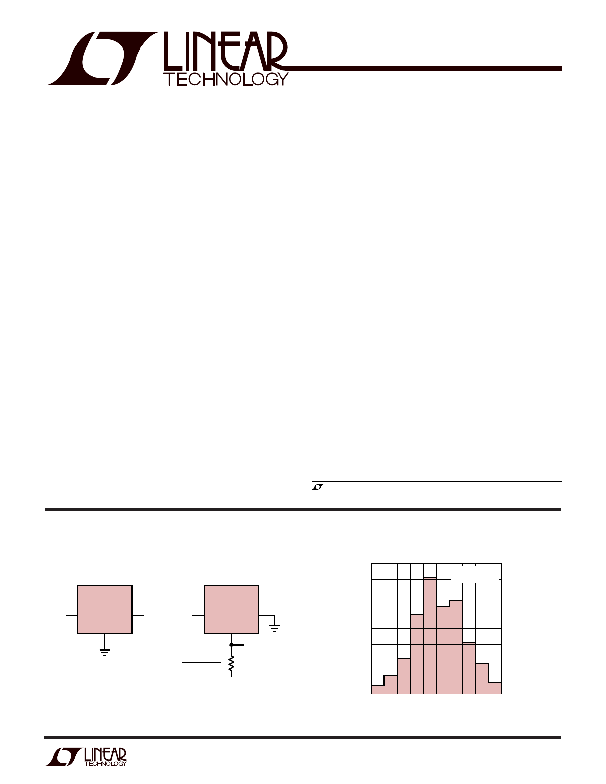
Typical Distribution of Temperature Drift
Basic Positive and Negative Connections
LT1021
IN
V
IN
OUT
GND
V
OUT
R1 =
NC
V
I
LOAD
OUT
LT1021
(7 AND 10 ONLY)
IN
GND
– (V–)
+ 1.5mA
–15V
(V
OUT
–V
OUT
R1
–
)
1021 TA01
24
21
18
15
12
UNITS (%)
9
6
3
– 0
–5
DISTRIBUTION
OF THREE RUNS
–3 –1 1 52–4 –2 0 4
OUTPUT DRIFT (ppm/°C)
3
1021 TA01
1
Page 2
LT1021
A
W
O
LUTEXI T
S
A
WUW
ARB
U
G
I
(Note 1)
S
Input Voltage .......................................................... 40V
Input/Output Voltage Differential ............................ 35V
Output-to-Ground Voltage (Shunt Mode Current Limit)
LT1021-5............................................................. 10V
LT1021-7............................................................. 10V
LT1021-10........................................................... 16V
Trim Pin-to-Ground Voltage
Positive ............................................... Equal to V
OUT
Negative ........................................................... – 20V
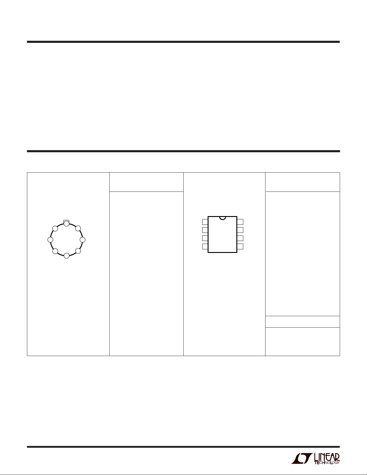
PACKAGE
/
O
RDER I FOR ATIO
WU
U
ORDER PART
NUMBER
LT1021BCH-5
TOP VIEW
NC*
8
1
NC*
2
V
IN
3
NC*
H PACKAGE
8-LEAD TO-5 METAL CAN
CONNECTED INTERNALLY.
*
D0 NOT CONNECT EXTERNAL
CIRCUITRY TO THESE PINS
NO TRIM PIN ON LT1021-7.
**
DO NOT CONNECT EXTERNAL
CIRCUITRY TO PIN 5 ON LT1021-7
T
= 150°C, θJA = 150°C/W,θJC = 45°C/W
JMAX
7
5
4
GND
NC*
6
TRIM
V
OUT
**
LT1021BMH-5
LT1021CCH-5
LT1021CMH-5
LT1021DCH-5
LT1021DMH-5
LT1021BCH-7
LT1021BMH-7
LT1021DCH-7
LT1021DMH-7
LT1021BCH-10
LT1021BMH-10
LT1021CCH-10
LT1021CMH-10
LT1021DCH-10
LT1021DMH-10
Output Short-Circuit Duration
VIN = 35V......................................................... 10 sec
VIN ≤ 20V ................................................... Indefinite
Operating Temperature Range
Commercial ............................................ 0°C to 70°C
Industrial ........................................... –40°C to 85°C
Military ............................................ –55°C to 125°C
Storage Temperature Range ................ –65°C to 150°C
Lead Temperature (Soldering, 10 sec)................ 300°C
ORDER PART
NUMBER
LT1021BCN8-5
TOP VIEW
DNC*
1
V
2
IN
DNC*
3
GND
4
N8 PACKAGE
8-LEAD PDIP
CONNECTED INTERNALLY.
*
D0 NOT CONNECT EXTERNAL
CIRCUITRY TO THESE PINS
NO TRIM PIN ON LT1021-7.
**
DO NOT CONNECT EXTERNAL
CIRCUITRY TO PIN 5 ON LT1021-7
T
= 130°C, θJA = 130°C/W (N)
JMAX
= 130°C, θJA = 150°C/W (S)
T
JMAX
S8 PACKAGE
8-LEAD PLASTIC SO
8
7
6
5
DNC*
DNC*
V
0UT
TRIM**
LT1021CCN8-5
LT1021CIN8-5
LT1021DCN8-5
LT1021DIN8-5
LT1021DCS8-5
LT1021BCN8-7
LT1021DCN8-7
LT1021DCS8-7
LT1021BCN8-10
LT1021CCN8-10
LT1021CIN8-10
LT1021DCN8-10
LT1021DCS8-10
LT1021DIN8-10
S8 PART MARKING
2
021DC5
021DC7
021DC1
Page 3

LT1021
LECTRICAL C CHARA TERIST
E
range, otherwise specifications are TA = 25°C. VIN = 10V, I
PARAMETER CONDITIONS MIN TYP MAX UNITS
Output Voltage (Note 2) LT1021C-5 4.9975 5.000 5.0025 V
Output Voltage Temperature Coefficient (Note 3) T
Line Regulation (Note 4) 7.2V ≤ VIN ≤ 10V 4 12 ppm/V
Load Regulation (Sourcing Current) 0 ≤ I
Load Regulation (Sinking Current) 0 ≤ I
Supply Current 0.8 1.2 mA
Output Voltage Noise (Note 6) 0.1Hz ≤ f ≤ 10Hz 3.0 µV
Long Term Stability of Output Voltage (Note 7) ∆t = 1000Hrs Noncumulative 15 ppm
Temperature Hysteresis of Output ∆T = ±25°C 10 ppm
ICS
LT1021B-5/LT1021D-5 4.9500 5.000 5.0500 V
≤ TJ ≤ T
MIN
LT1021B-5 ● 2 5 ppm/°C
LT1021C-5/LT1021D-5 ● 3 20 ppm/°C
10V ≤ V
OUT
(Note 4)
OUT
(Note 4)
10Hz ≤ f ≤ 1kHz 2.2 3.5 µV
The ● denotes specifications that apply over the full operating temperature
= 0, unless otherwise noted.
OUT
LT1021-5
MAX
● 20 ppm/V
≤ 40V 2 6 ppm/V
IN
≤ 10mA 10 20 ppm/mA
≤ 10mA 60 100 ppm/mA
● 10 ppm/V
● 35 ppm/mA
● 150 ppm/mA
● 1.5 mA
P-P
RMS
The ● denotes specifications that apply over the full operating temperature range, otherwise specifications are TA = 25°C.
VIN = 12V, I
PARAMETER CONDITIONS MIN TYP MAX UNITS
Output Voltage (Note 2) 6.95 7.00 7.05 V
Output Voltage Temperature Coefficient (Note 3) T
Line Regulation (Note 4) 8.5V ≤ VIN ≤ 12V 1.0 4 ppm/V
Load Regulation (Sourcing Current) 0 ≤ I
Load Regulation (Shunt Mode) 1.2mA ≤ I
Supply Current (Series Mode) 0.75 1.2 mA
Minimum Current (Shunt Mode) VIN is Open 0.7 1.0 mA
Output Voltage Noise (Note 6) 0.1Hz ≤ f ≤ 10Hz 4.0 µV
Long Term Stability of Output Voltage (Note 7) ∆t = 1000Hrs Noncumulative 7 ppm
Temperature Hysteresis of Output ∆T = ±25°C 3 ppm
= 0, unless otherwise noted.
OUT
LT1021-7
≤ TJ ≤ T
MIN
LT1021B-7 ● 2 5 ppm/°C
LT1021D-7
12V ≤ V
(Note 4)
(Notes 4, 5)
10Hz ≤ f ≤ 1kHz 2.5 4.0 µV
MAX
● 3 20 ppm/°C
● 2.0 8 ppm/V
≤ 40V 0.5 2 ppm/V
IN
≤ 10mA 12 25 ppm/mA
OUT
≤ 10mA 50 100 ppm/mA
SHUNT
● 1.0 4 ppm/V
● 40 ppm/mA
● 150 ppm/mA
● 1.5 mA
● 1.2 mA
P-P
RMS
3
Page 4

LT1021
LECTRICAL C CHARA TERIST
E
range, otherwise specifications are TA = 25°C. VIN = 15V, I
PARAMETER CONDITIONS MIN TYP MAX UNITS
Output Voltage (Note 2) LT1021C-10 9.995 10.00 10.005 V
Output Voltage Temperature Coefficient (Note 3) T
Line Regulation (Note 4) 11.5V ≤ VIN ≤ 14.5V 1.0 4 ppm/V
Load Regulation (Sourcing Current) 0 ≤ I
Load Regulation (Shunt Mode) 1.7mA ≤ I
Supply Current (Series Mode) 1.2 1.7 mA
Minimum Current (Shunt Mode) VIN is Open 1.1 1.5 mA
Output Voltage Noise (Note 6) 0.1Hz ≤ f ≤ 10Hz 6.0 µV
Long Term Stability of Output Voltage (Note 7) ∆t = 1000Hrs Noncumulative 15 ppm
Temperature Hysteresis of Output ∆T = ±25°C 5 ppm
ICS
LT1021B-10/LT1021D-10 9.950 10.00 10.050 V
≤ TJ ≤ T
MIN
LT1021B-10 ● 2 5 ppm/°C
LT1021C-10/LT1021D-10 ● 5 20 ppm/°C
14.5V ≤ V
OUT
(Note 4)
(Notes 4, 5)
10Hz ≤ f ≤ 1kHz 3.5 6 µV
The ● denotes specifications that apply over the full operating temperature
= 0, unless otherwise noted.
OUT
LT1021-10
MAX
● 6 ppm/V
≤ 40V 0.5 2 ppm/V
IN
≤ 10mA 12 25 ppm/mA
≤ 10mA 50 100 ppm/mA
SHUNT
● 4 ppm/V
● 40 ppm/mA
● 150 ppm/mA
● 2.0 mA
● 1.7 mA
P-P
RMS
Note 1: Absolute Maximum Ratings are those values beyond which the life
of a device may be impaired.
Note 2: Output voltage is measured immediately after turn-on. Changes
due to chip warm-up are typically less than 0.005%.
Note 3: Temperature coefficient is measured by dividing the change in
output voltage over the temperature range by the change in temperature.
Separate tests are done for hot and cold; T
Incremental slope is also measured at 25°C.
Note 4: Line and load regulation are measured on a pulse basis. Output
changes due to die temperature change must be taken into account
separately. Package thermal resistance is 150°C/W for TO-5 (H), 130°C/W
for N and 150°C/W for the SO-8.
to 25°C and 25°C to T
MIN
MAX
.
Note 5: Shunt mode regulation is measured with the input open. With the
input connected, shunt mode current can be reduced to 0mA. Load
regulation will remain the same.
Note 6: RMS noise is measured with a 2-pole highpass filter at 10Hz and a
2-pole lowpass filter at 1kHz. The resulting output is full-wave rectified and
then integrated for a fixed period, making the final reading an average as
opposed to RMS. Correction factors are used to convert from average to
RMS and correct for the non-ideal bandpass of the filters.
Peak-to-peak noise is measured with a single highpass filter at 0.1Hz and a
2-pole lowpass filter at 10Hz. The unit is enclosed in a still-air environment
to eliminate thermocouple effects on the leads. Test time is 10 seconds.
Note 7: Consult factory for units with long term stability data.
4
Page 5

LPER
OUTPUT CURRENT (mA)
0
INPUT/OUTPUT VOLTAGE (V)
1.2
1.6
16
1021 G03
0.8
0.4
0
4
8
12
20
1.0
1.4
0.6
0.2
14
2
6
10
18
TJ = 125 °C
TJ = –55 °C
TJ = 25 °C
FREQUENCY (Hz)
100
NOISE VOLTAGE (nV/√Hz)
200
250
350
400
10 1k 10k
LT1021 G06
0
100
300
150
50
LT1021-10
LT1021-5
LT1021-7
Ripple Rejection
115
f = 150Hz
110
105
100
REJECTION (dB)
95
90
85
0
13
12
11
10
9
8
7
6
OUTPUT VOLTAGE (V)
5
4
3
10 20
515
INPUT VOLTAGE (V)
Start-Up (Series Mode)
VIN = 0V TO 12V
04
2
F
LT1021-10
LT1021-7
LT1021-5
6
TIME (µs)
R
O
LT1021-7
LT1021-10
LT1021-5
25
8
LT1021
UW
ATYPICA
30
10
35
LT1021 G01
12
LT1021 G04
40
14
CCHARA TERIST
E
C
Ripple Rejection
130
VIN = 15V
= 0
C
OUT
120
110
100
90
80
REJECTION (dB)
70
60
50
10
Start-Up (Shunt Mode)
LT1021-7, LT1021-10
11
10
9
8
7
OUTPUT VOLTAGE (V)
6
5
02
ICS
LT1021-7
LT1021-10
LT1021-5
100 1k 10k
FREQUENCY (Hz)
LT1021-10
+ 2V
V
OUT
0V
NC
LT1021-7
61012
48
TIME (µs)
LT1021 G02
1k
V
OUT
OUT
IN
GND
LT1021 G05
Minimum Input/Output Differential
LT1021-7, LT1021-10
Output Voltage Noise Spectrum
Output Voltage Noise
16
C
= 0
OUT
FILTER = 1 POLE
14
= 0.1Hz
f
LOW
12
10
8
6
RMS NOISE (µV)
4
2
0
10
LT1021-10
100 1k 10k
BANDWIDTH (Hz)
LT1021-7
LT1021-5
LT1021 G07
Output Voltage Temperature Drift
LT1021-5
5.006
5.004
5.002
5.000
4.998
OUTPUT VOLTAGE (V)
4.996
4.994
–50
0
–25
TEMPERATURE (°C)
50
25
Load Regulation LT1021-5
5
VIN = 8V
4
3
2
1
0
–1
–2
OUTPUT CHANGE (mV)
–3
–4
100
LT1021 G08
125
75
–5
–6–8 –4 0 4 8
–10
–2
SOURCING SINKING
OUTPUT CURRENT (mA)
2
6
10
LT1021 G09
5
Page 6

LT1021
TIME (MINUTES)
035
LT1021 G15
12
46
OUTPUT VOLTAGE NOISE (5µV/DIV)
5µV (1ppm)
FILTERING = 1 ZERO AT 0.1Hz
2 POLES AT 10Hz
LPER
Quiescent Current LT1021-5
1.8
1.6
1.4
1.2
1.0
0.8
0.6
INPUT CURRENT (mA)
0.4
0.2
= 0
I
OUT
TJ = –55°C
TJ = 25°C
TJ = 125°C
0
5 10152025 40
0
INPUT VOLTAGE (V)
F
O
R
ATYPICA
3530
LT1021 G10
UW
CCHARA TERIST
E
C
Sink Mode* Current Limit
LT1021-5
60
VIN = 8V
50
40
30
20
CURRENT INTO OUTPUT (mA)
10
0
26
4
0
*NOTE THAT AN INPUT VOLTAGE IS REQUIRED
FOR 5V UNITS.
ICS
10 18
12
8
OUTPUT VOLTAGE (V)
14
16
LT1021 G11
Thermal Regulation LT1021-5
VIN = 25V
∆POWER = 200mW
0
–0.5
–1.0
OUTPUT CHANGE (mV)
LOAD
REGULATION
I
LOAD
0
20
= 10mA
40
TIME (ms)
60
THERMAL
REGULATION
80
100
120
LT1021 G12
140
Load Transient Response
LT1021-5, C
I
SOURCE
I
SOURCE
I
SOURCE
OUTPUT CHANGE (50mV/DIV)
∆I
SOURCE
Output Voltage Temperature
Drift LT1021-7
7.003
7.002
7.001
7.000
6.999
OUTPUT VOLTAGE (V)
6.998
6.997
–50
–25
= 0
LOAD
= 0
50mV 50mV
= 0.5mA
= 2-10mA
= 100µA
102413
0
TEMPERATURE (°C)
P-P
3
TIME (µs)
25
I
SINK
I
SINK
∆I
SINK
0
50
= 0
I
SINK
= 2-10mA
= 100µA
75
= 0.2mA
2
LT1021 G13
100
LT1021 G16
P-P
4
125
Load Transient Response
LT1021-5, C
I
SOURCE
I
SOURCE
OUTPUT CHANGE (20mV/DIV)
∆I
SOURCE
LOAD
= 0
20mV 20mV
I
= 0.2mA
SOURCE
= 2-10mA
= 100µA
P-P
501020515
15
TIME (µs)
Load Regulation
LT1021-7, LT1021-10
5
VIN = 12V
4
3
2
1
0
–1
–2
OUTPUT CHANGE (mV)
–3
–4
–5
–6–8 –4 0 4 8
–10
SOURCING SINKING
–2
OUTPUT CURRENT (mA)
= 1000pF
I
= 0
SINK
I
SINK
I
SINK
∆I
SINK
0
2
= 0.2mA
= 2-10mA
= 100µA
10
LT1021 G14
6
LT1021 G17
P-P
Output Noise 0.1Hz to 10Hz
LT1021-5
20
Quiescent Current LT1021-7
1.8
1.6
1.4
1.2
1.0
0.8
0.6
INPUT CURRENT (mA)
0.4
0.2
10
= 0
I
OUT
TJ = –55°C
TJ = 25°C
TJ = 125°C
0
5 10152025 40
0
INPUT VOLTAGE (V)
3530
LT1021 G18
6
Page 7

LPER
TIME (MINUTES)
035
LT1021 G24
12
46
OUTPUT VOLTAGE NOISE (5µV/DIV)
5µV (0.7ppm)
FILTERING = 1 ZERO AT 0.1Hz
2 POLES AT 10Hz
F
O
Shunt Characteristics LT1021-7
1.2
INPUT PIN OPEN
1.0
0.8
0.6
0.4
CURRENT INTO OUTPUT (mA)
0.2
TJ = 25°C
TJ = –55°C
T
= 125°C
J
R
ATYPICA
UW
CCH ARA TERIST
E
C
Shunt Mode Current Limit
LT1021-7 Thermal Regulation LT1021-7
60
INPUT PIN OPEN
50
40
30
20
CURRENT INTO OUTPUT (mA)
10
ICS
VIN = 27V
∆POWER = 200mW
0
–0.5
–1.0
–1.5
OUTPUT CHANGE (mV)
LOAD
REGULATION
I
LOAD
= 10mA
LT1021
THERMAL
REGULATION*
0
13
0
OUTPUT TO GROUND VOLTAGE (V)
Load Transient Response
LT1021-7, C
I
SOURCE
5mV
I
SOURCE
OUTPUT VOLTAGE CHANGE
I
SOURCE
∆I
SOURCE
102413
NOTE VERTICAL SCALE CHANGE
BETWEEN SOURCING AND SINKING
Output Voltage Temperature
Drift LT1021-10
10.006
10.004
10.002
10.000
9.998
OUTPUT VOLTAGE (V)
9.996
9.994
–50
–25
2
LOAD
= 0
= 0.5mA
= 2-10mA
= 100µA
3
TIME (µs)
0
TEMPERATURE (°C)
7
59
6
4
8
1021 G19
= 0
I
= 0.8mA
SINK
I
= 1.2mA
SINK
50mV
I
= 1.4mA
SINK
I
= 2-10mA
SINK
= 100µA
∆I
P-P
SINK
0
50
25
P-P
2
4
LT1021 G22
100
LT1021 G25
125
75
0
26
4
0
8
OUTPUT VOLTAGE (V)
Load Transient Response
LT1021-7, C
I
SOURCE
OUTPUT VOLTAGE CHANGE
∆I
SOURCE
NOTE VERTICAL SCALE CHANGE
BETWEEN SOURCING AND SINKING
LOAD
= 0
5mV
I
= 0.5mA
SOURCE
I
= 2-10mA
SOURCE
= 100µA
P-P
501020515
15
5µs/DIV
Load Regulation
LT1021-7, LT1021-10
5
VIN = 12V
4
3
2
1
0
–1
–2
OUTPUT CHANGE (mV)
–3
–4
–5
–6–8 –4 0 4 8
–10
SOURCING SINKING
–2
OUTPUT CURRENT (mA)
14
10 18
16
12
LT1021 G20
= 1000pF
I
= 0.6mA
SINK
20mV
I
= 0.8mA
SINK
= 1mA
I
SINK
I
= 2-10mA
SINK
∆I
= 100µA
SINK
0
10
LT1021 G23
2
6
P-P
1021 G26
60
TIME (ms)
80
100
0
20
40
*INDEPENDENT OF TEMPERATURE COEFFICIENT
120
LT1021 G21
140
Output Noise 0.1Hz to 10Hz
LT1021-7
20
Input Supply Current LT1021-10
1.8
1.6
1.4
1.2
1.0
0.8
0.6
INPUT CURRENT (mA)
0.4
0.2
10
= 0
I
OUT
0
5 10152025 40
0
TJ = –55°C
TJ = 25°C
TJ = 125°C
INPUT VOLTAGE (V)
3530
1021 G27
7
Page 8

LT1021
LPER
Shunt Characteristics LT1021-10
1.8
INPUT PIN OPEN
1.6
1.4
1.2
1.0
0.8
0.6
0.4
CURRENT INTO OUTPUT (mA)
0.2
0
TJ = –55°C
0
OUTPUT TO GROUND VOLTAGE (V)
F
O
TJ = 125°C
42 6 10 12
8
R
ATYPICA
TJ = 25°C
1021 G28
UW
CCH ARA TERIST
E
C
Shunt Mode Current Limit
LT1021-10 Thermal Regulation LT1021-10
60
INPUT PIN OPEN
50
40
30
20
CURRENT INTO OUTPUT (mA)
10
0
26
4
0
ICS
10 18
12
8
OUTPUT VOLTAGE (V)
VIN = 30V
∆POWER = 200mW
0
–0.5
–1.0
–1.5
OUTPUT CHANGE (mV)
14
16
1021 G29
*INDEPENDENT OF TEMPERATURE COEFFICIENT
REGULATION
I
LOAD
0
20
LOAD
= 10mA
40
TIME (ms)
THERMAL
REGULATION*
60
80
100
120
1021 G30
140
Load Transient Response
LT1021-10, C
I
= 0
SOURCE
10mV
I
= 0.2mA
SOURCE
OUTPUT VOLTAGE CHANGE
I
SOURCE
∆I
= 100µA
SOURCE
102413
NOTE VERTICAL SCALE CHANGE
BETWEEN SOURCING AND SINKING
LOAD
= 2-10mA
P-P
3
TIME (µs)
= 0
I
SINK
I
SINK
∆I
SINK
0
= 0.6mA
50mV
I
SINK
I
= 1mA
SINK
= 2-10mA
= 100µA
= 0.8mA
2
1021 G31
P-P
4
Load Transient Response
LT1021-10, C
I
= 0
SOURCE
5mV
I
= 0.5mA
SOURCE
OUTPUT VOLTAGE CHANGE
I
SOURCE
∆I
= 100µA
SOURCE
102413
NOTE VERTICAL SCALE CHANGE
BETWEEN SOURCING AND SINKING
LOAD
I
SINK
= 2-10mA
P-P
3
TIME (µs)
= 1000pF
I
SINK
= 1.2mA
I
∆I
SINK
0
= 0.8mA
20mV
I
SINK
= 2-10mA
SINK
= 100µA
= 1.4mA
2
1021 G32
P-P
4
Output Noise 0.1Hz to 10Hz
LT1021-10
FILTERING = 1 ZERO AT 0.1Hz
OUTPUT VOLTAGE NOISE (10µV/DIV)
035
2 POLES AT 10Hz
10µV (1ppm)
12
TIME (MINUTES)
46
1021 G33
8
Page 9

LT1021
U
WUU
APPLICATIONS IN FORMA TION
Effect of Reference Drift on System Accuracy
A large portion of the temperature drift error budget in
many systems is the system reference voltage. This graph
indicates the maximum temperature coefficient allowable
if the reference is to contribute no more than 0.5LSB error
to the overall system performance. The example shown is
a 12-bit system designed to operate over a temperature
range from 25°C to 65°C. Assuming the system calibration is performed at 25°C, the temperature span is 40°C.
It can be seen from the graph that the temperature coefficient of the reference must be no worse than 3ppm/°C if
it is to contribute less than 0.5LSB error. For this reason,
the LT1021 family has been optimized for low drift.
Maximum Allowable Reference Drift
100
8-BIT
The LT1021-10 “C” version is pre-trimmed to ±5mV and
therefore can utilize a restricted trim range. A 75k resistor
in series with a 20kΩ potentiometer will give ±10mV trim
range. Effect on the output TC will be only 1ppm/°C for the
±5mV trim needed to set the “C” device to 10.000V.
LT1021-5
The LT1021-5 does have an output voltage trim pin, but
the TC of the nominal 4V open-circuit voltage at this pin is
about –1.7mV/°C. For the voltage trimming not to affect
reference output TC, the external trim voltage must track
the voltage on the trim pin. Input impedance of the trim pin
is about 100kΩ and attenuation to the output is 13:1. The
technique shown below is suggested for trimming the
output of the LT1021-5 while maintaining minimum shift
in output temperature coefficient. The R1/R2 ratio is
chosen to minimize interaction of trimming and TC shifts,
so the exact values shown should be used.
10-BIT
10
0.5LSB ERROR (ppm/°C)
MAXIMUM TEMPERATURE COEFFICIENT FOR
1.0
100
12-BIT
14-BIT
20 100
40
50
30
TEMPERATURE SPAN (°C)
807060
90
LT1021 AI01
Trimming Output Voltage
LT1021-10
The LT1021-10 has a trim pin for adjusting output voltage.
The impedance of the trim pin is about 12kΩ with a
nominal open-circuit voltage of 5V. It is designed to be
driven from a source impedance of 3kΩ or less to minimize changes in the LT1021 TC with output trimming.
Attenuation between the trim pin and the output is 70:1.
This allows ±70mV trim range when the trim pin is tied to
the wiper of a potentiometer connected between the
output and ground. A 10kΩ potentiometer is recommended, preferably a 20 turn cermet type with stable
characteristics over time and temperature.
LT1021-5
IN
GND
OUT
TRIM
R1
27k
1N4148
V
R2
50k
1021 AI02
OUT
LT1021-7
The 7V version of the LT1021 has no trim pin because the
internal architecture does not have a point which could be
driven conveniently from the output. Trimming must
therefore be done externally, as is the case with ordinary
reference diodes. Unlike these diodes, however, the output of the LT1021 can be loaded with a trim potentiometer.
The following trim techniques are suggested; one for
voltage output and one for current output. The voltage
output is trimmed for 6.95V. Current output is 1mA, as
shown, into a summing junction, but all resistors may be
scaled for currents up to 10mA.
Both of these circuits use the trimmers in a true potentiometric mode to reduce the effects of trimmer TC. The
voltage output has a 200Ω impedance, so loading must be
9
Page 10

LT1021
U
WUU
APPLICATIONS IN FORMA TION
minimized. In the current output circuit, R1 determines
output current. It should have a TC commensurate with the
LT1021 or track closely with the feedback resistor around
the op amp.
LT1021-7
IN
LT1021-7
IN
GND
OUT
GND
50k
OUT
R3
R3
10k
TC TRACKING TO 50ppm/°C
R2**
182k
R2*
14k
1%
R1*
7.15k
1.000mA
R1*
200Ω
1%
V
OUT
6.950V
1021 AI03
Kelvin Connections
Although the LT1021 does not have true force/sense
capability at its outputs, significant improvements in ground
loop and line loss problems can be achieved with proper
hook-up. In series mode operation, the ground pin of the
LT1021 carries only ≈1mA and can be used as a sense
line, greatly reducing ground loop and loss problems on
the low side of the reference. The high side supplies load
current so line resistance must be kept low. Twelve feet of
#22 gauge hook-up wire or 1 foot of 0.025 inch printed
circuit trace will create 2mV loss at 10mA output current.
This is equivalent to 1LSB in a 10V, 12-bit system.
The following circuits show proper hook-up to minimize
errors due to ground loops and line losses. Losses in the
output lead can be greatly reduced by adding a PNP boost
transistor if load currents are 5mA or higher. R2 can be
added to further reduce current in the output sense lead.
Standard Series Mode
–
OP AMP
+
1021 AI04
RESISTOR TC DETERMINES I
*
TC ≤ (10 • R1) TC. R2 AND R3 SCALE
**
WITH R1 FOR DIFFERENT OUTPUT CURRENTS
OUT
TC
Capacitive Loading and Transient Response
The LT1021 is stable with all capacitive loads, but for
optimum settling with load transients, output capacitance
should be under 1000pF. The output stage of the reference
is class AB with a fairly low idling current. This makes
transient response worst-case at light load currents. Because of internal current drain on the output, actual worstcase occurs at I
–0.8mA (sinking) on LT1021-7 and I
= 0 on LT1021-5, I
LOAD
LOAD
=
LOAD
= 1.4mA (sinking) on LT1021-10. Significantly better load transient
response is obtained by moving slightly away from these
points. See Load Transient Response curves for details. In
general, best transient response is obtained when the
output is sourcing current. In critical applications, a 10µ F
solid tantalum capacitor with several ohms in series
provides optimum output bypass.
INPUT
GROUND
RETURN
LT1021
IN
GND
KEEP THIS LINE RESISTANCE LOW
OUT
Series Mode with Boost Transistor
INPUT
R1
220Ω
2N3906
IN
LT1021
OUT
GND
GROUND
RETURN
*OPTIONAL—REDUCES CURRENT IN OUTPUT SENSE LEAD
R2 = 2.4k (LT1021-5), 3k (LT1021-7), 5.6k (LT1021-10)
R2*
1021 AI06
+
LOAD
1021 AI05
LOAD
10
Page 11

LT1021
U
WUU
APPLICATIONS IN FORMA TION
Effects of Air Movement on Low Frequency Noise
The LT1021 has very low noise because of the buried zener
used in its design. In the 0.1Hz to 10Hz band, peak-to-peak
noise is about 0.5ppm of the DC output. To achieve this
low noise, however, care must be taken to shield the
reference from ambient air turbulence. Air movement can
create noise because of thermoelectric differences
between IC package leads (especially kovar lead TO-5) and
printed circuit board materials and/or sockets. Power
dissipation in the reference, even though it rarely exceeds
20mW, is enough to cause small temperature gradients in
the package leads. Variations in thermal resistance, caused
by uneven air flow, create differential lead temperatures,
thereby causing thermoelectric voltage noise at the output
of the reference. The following XY plotter trace dramatically illustrates this effect. The first half of the plot was
done with the LT1021 shielded from ambient air with a
small foam cup. The cup was then removed for the second
half of the trace. Ambient in both cases was a lab environment with no excessive air turbulence from air conditioners, opening/closing doors, etc. Removing the foam cup
increases the output noise by almost an order of magnitude in the 0.01Hz to 1Hz band! The kovar leads of the
TO-5 (H) package are the primary culprit. Alloy 42 and
copper lead frames used on dual-in-line packages are not
nearly as sensitive to thermally generated noise because
they are intrinsically matched.
There is nothing magical about foam cups—any enclosure which blocks air flow from the reference will do.
Smaller enclosures are better since they do not allow the
build-up of internally generated air movement. Naturally,
heat generating components external to the reference
itself should not be included inside the enclosure.
Noise Induced By Air Turbulence (TO-5 Package)
LT1021-7 (TO-5 PACKAGE)
f = 0.01Hz TO 10Hz
20µV
OUTPUT VOLTAGE NOISE (20µV/DIV)
0610
24
TIME (MINUTES)
FOAM CUP
REMOVED
812
1021 AI07
U
TYPICAL APPLICATIONS
Restricted Trim Range for Improved
Resolution, 10V, “C” Version Only
LT1021C-10
IN 10.000V
IN
OUT V
GND TRIM
TRIM RANGE ≈ ±10mV
R1
75k
R2
50k
1021 TA11
LT1021-10
V
IN
GND
OUT
TRIM
IN
*CAN BE RAISED TO 20k FOR
LESS CRITICAL APPLICATIONS
R1*
10k
1021 TA03
Negative Series ReferenceLT1021-10 Full Trim Range (±0.7%)
15V
V
OUT
4.7k
–15V
R1
4.7k
R2
Q1
2N2905
D1
15V
LT1021-10
IN
GND
LT1021 TA04
OUT
–10V AT 50mA
11
Page 12

LT1021
LT1021-10
OUT
IN
TRIM
GND
4.32k
V
OUT
= 10.24V
V
IN
5k
V
–
= –15V*
*MUST BE WELL REGULATED
dV
OUT
dV
–
=
15mV
V
1021 TA12
TYPICAL APPLICATIONS
U
Boosted Output Current
with No Current Limit
+
≥ (V
OUT
+ 1.8V)
LT1021
V
2-Pole Lowpass Filtered Reference
LT1021
IN
V
IN
OUT
GND
IN
GND
R1
220Ω
OUT
R1
36k
+
f = 10Hz
2N2905
10V AT
100mA
2µF
SOLID
TANT
1021 TA05
1µF
MYLAR
R2
36k
+
V
–
LT1001
+
0.5µF
MYLAR
Boosted Output Current
with Current Limit
≥ V
+ 2.8V
OUT
*GLOWS IN CURRENT LIMIT,
DO NOT OMIT
V
IN
TOTAL NOISE
≤2µV
RMS
1Hz ≤ f ≤ 10kHz
D1*
LED
V
LT1021
REF
IN
GND
Ultraprecise Current Source
R1
220Ω
OUT
+
8.2Ω
15V
2N2905
10V AT
100mA
2µF
SOLID
TANT
1021 TA06
LT1021-7
IN
OUT
GND
6
Operating 5V Reference from 5V Supply
C1*
5µF
+
1N914
1N914
+
CMOS LOGIC GATE**
≥ 2kHz*
f
IN
FOR HIGHER FREQUENCIES C1 AND C2 MAY BE DECREASED
*
PARALLEL GATES FOR HIGHER REFERENCE CURRENT LOADING
**
TRIM
100Ω
≈8.5V
C2*
5µF
17.4k
1%
15V
7
–
2
LT1001
–15V
3
+
4
I
REGULATION < 1ppm/V
COMPLIANCE = –13V TO 7V
LT1021-5
IN
OUT
GND
OUT
6.98k*
0.1%
*LOW TC
= 1mA
5V LOGIC
SUPPLY
5V
REFERENCE
1021 TA07
1021 TA16
LT1021-10
12
OUT
GND
–15V
TRIM
1.2k
–V
REF
1021 TA13
CMOS DAC with Low Drift Full-Scale Trimming**
4.02K
R1
4.99k
1%
R2
40.2Ω
1%
*
TC LESS THAN 200ppm/°C
**
NO ZERO ADJUST REQUIRED
WITH LT1007 (V
REF
7520, ETC
CMOS
DAC
0S
FB
≤ 60µV)
I
OUT
30pF
–
LT1007C
+
R3
1%
R4*
100Ω
FULL-SCALE
ADJUST
10V
F.S.
LT1236 TA15
Trimming 10V Units to 10.24V
Page 13

U
LT1021-10
OUT
GND
IN
1021 TA08
R
L
30mA
15V
R1*
169Ω
V
OUT
10V
TYPICAL LOAD
CURRENT = 30mA
SELECT R1 TO DELIVER TYPICAL LOAD CURRENT.
LT1021 WILL THEN SOURCE OR SINK AS NECESSARY
TO MAINTAIN PROPER OUTPUT. DO NOT REMOVE LOAD
AS OUTPUT WILL BE DRIVEN UNREGULATED HIGH. LINE
REGULATION IS DEGRADED IN THIS APPLICATION
*
TYPICAL APPLICATIONS
LT1021
Strain Gauge Conditioner for 350Ω Bridge
R1
357Ω
1/2W
LM301A
1
100pF
OF AMPLIFIER
IN
28mA
+
†
–
8
28.5mA
3
2
LT1021-10
15V
THIS RESISTOR PROVIDES POSITIVE FEEDBACK TO
*
THE BRIDGE TO ELIMINATE LOADING EFFECT OF
THE AMPLIFIER. EFFECTIVE Z
STAGE IS ≥1MΩ. IF R2 TO R5 ARE CHANGED,
SET R6 = R3
IN
OUT
GND
6 6
5V
350Ω STRAIN
GAUGE BRIDGE**
R2
20k
R4
20k
R5
2M
–5V
357Ω
1/2W
–15V
BRIDGE IS ULTRALINEAR WHEN ALL LEGS ARE
**
ACTIVE, TWO IN COMPRESSION AND TWO IN TENSION,
OR WHEN ONE SIDE IS ACTIVE WITH ONE COMPRESSED
AND ONE TENSIONED LEG
†
OFFSET AND DRIFT OF LM301A ARE VIRTUALLY
ELIMINATED BY DIFFERENTIAL CONNECTION OF LT1012C
2
3
–
LT1012C
+
R6*
2M
R3
2M
1021 TA09
Negative Shunt Reference Driven
by Current Source
LT1021-10
OUT
GND
V
OUT
×100
LM334
–11V TO –40V
2.5mA
–10V (I
LOAD
27Ω
≤ 1mA)
1021 TA14
Precision DAC Reference with System TC Trim
LT1021-10
15V
IN
OUT
GND
TRIMS 1mA REFERENCE CURRENT
*
TC BY ±40ppm/°C. THIS TRIM SCHEME HAS
VERY LITTLE EFFECT ON ROOM TEMPERATURE
CURRENT TO MINIMIZE ITERATIVE TRIMMING
8.87k
1%
1.24k
1%
D1
1N457
50k
TC TRIM*
10k
1%
10k
1%
D2
1N457
50k
50k
ROOM TEMP
TRIM
200k
1%
10.36k
1%
1mA
Handling Higher Load Currents
8.45k
DAC
1021 TA17
13
Page 14

LT1021
TYPICAL APPLICATIONS
U
Ultralinear Platinum Temperature Sensor*
LT1021-10
IN
OUT
20V
100k
R2*
5k
R1**
253k
R8
R9
10M
–15V
R3**
5k
R7
392k
1%
†
R
S
100Ω AT
0°C
R10
182k
1%
R4
4.75k
1%
GND
R14
5k
R11
6.65M
1%
2
R5
200k
1%
3
R6
†
619k
STANDARD INDUSTRIAL 100Ω PLATINUM 4-WIRE SENSOR,
1%
ROSEMOUNT 78S OR EQUIVALENT. α = 0.00385
TRIM R9 FOR V
TRIM R12 FOR V
TRIM R14 FOR V
USE TRIM SEQUENCE AS SHOWN. TRIMS ARE NONINTERACTIVE
SO THAT ONLY ONE TRIM SEQUENCE IS NORMALLY REQUIRED.
*
FEEDBACK LINEARIZES OUTPUT TO ±0.005°C FROM
–50°C TO 150°C
**
WIREWOUND RESISTORS WITH LOW TC
–
LT1001
+
R
654k
20V
–15V
**
F
7
4
6
= 0V AT 0°C
OUT
= 10V AT 100°C
OUT
= 5V AT 50°C
OUT
R15
10k
R13
24.3k
R12
1k
=100mV/°C
V
OUT
–50°C ≤ T ≤ 150°C
1021 TA10
U
W
EQUIVALE T SCHE ATIC
D4
6.3V
INPUT
Q3
D1
D2
OUTPUT
D3
R1
Q1
+
–
A1
Q2
R2
LT1021 ES
GND
14
Page 15

PACKAGE DESCRIPTION
SEATING
PLANE
0.010 – 0.045*
(0.254 – 1.143)
45°TYP
U
Dimensions in inches (millimeters) unless otherwise noted.
H Package
8-Lead TO-5 Metal Can (0.200 PCD)
(LTC DWG # 05-08-1320)
0.335 – 0.370
(8.509 – 9.398)
DIA
0.305 – 0.335
(7.747 – 8.509)
0.016 – 0.021**
(0.406 – 0.533)
0.050
(1.270)
MAX
0.027 – 0.045
(0.686 – 1.143)
PIN 1
GAUGE
PLANE
0.200
(5.080)
TYP
0.165 – 0.185
(4.191 – 4.699)
0.500 – 0.750
(12.700 – 19.050)
REFERENCE
PLANE
0.028 – 0.034
(0.711 – 0.864)
0.040
(1.016)
MAX
LT1021
0.110 – 0.160
(2.794 – 4.064)
INSULATING
STANDOFF
*
**
N8 Package
8-Lead PDIP (Narrow 0.300)
(LTC DWG # 05-08-1510)
876
0.255 ± 0.015*
(6.477 ± 0.381)
12
0.300 – 0.325
(7.620 – 8.255)
0.065
(1.651)
0.009 – 0.015
(0.229 – 0.381)
+0.035
0.325
–0.015
+0.889
8.255
()
–0.381
*THESE DIMENSIONS DO NOT INCLUDE MOLD FLASH OR PROTRUSIONS.
MOLD FLASH OR PROTRUSIONS SHALL NOT EXCEED 0.010 INCH (0.254mm)
TYP
0.045 – 0.065
(1.143 – 1.651)
0.100
(2.54)
BSC
LEAD DIAMETER IS UNCONTROLLED BETWEEN THE REFERENCE PLANE
AND 0.045" BELOW THE REFERENCE PLANE
FOR SOLDER DIP LEAD FINISH, LEAD DIAMETER IS
0.400*
(10.160)
MAX
5
4
3
0.130 ± 0.005
(3.302 ± 0.127)
0.125
0.020
(3.175)
MIN
(0.508)
0.018 ± 0.003
(0.457 ± 0.076)
MIN
N8 1098
0.016 – 0.024
(0.406 – 0.610)
H8(TO-5) 0.200 PCD 1197
Information furnished by Linear Technology Corporation is believed to be accurate and reliable.
However, no responsibility is assumed for its use. Linear Technology Corporation makes no representation that the interconnection of its circuits as described herein will not infringe on existing patent rights.
15
Page 16

LT1021
PACKAGE DESCRIPTION
U
Dimensions in inches (millimeters) unless otherwise noted.
S8 Package
8-Lead Plastic Small Outline (Narrow 0.150)
(LTC DWG # 05-08-1610)
0.189 – 0.197*
(4.801 – 5.004)
7
8
5
6
0.228 – 0.244
(5.791 – 6.197)
0.010 – 0.020
(0.254 – 0.508)
0.008 – 0.010
(0.203 – 0.254)
*
DIMENSION DOES NOT INCLUDE MOLD FLASH. MOLD FLASH
SHALL NOT EXCEED 0.006" (0.152mm) PER SIDE
**
DIMENSION DOES NOT INCLUDE INTERLEAD FLASH. INTERLEAD
FLASH SHALL NOT EXCEED 0.010" (0.254mm) PER SIDE
× 45°
(1.346 – 1.752)
0°– 8° TYP
0.016 – 0.050
0.406 – 1.270
0.053 – 0.069
0.014 – 0.019
(0.355 – 0.483)
0.150 – 0.157**
(3.810 – 3.988)
1
3
2
4
0.004 – 0.010
(0.101 – 0.254)
0.050
(1.270)
TYP
SO8 0996
RELATED PARTS
PART NUMBER DESCRIPTION COMMENTS
LT1019 Precision Bandgap Reference 0.05%, 5ppm/°C
LT1027 Precision 5V Reference 0.02%, 2ppm/°C
LT1236 Precision Reference SO-8, 5V and 10V, 0.05%, 5ppm/°C
LTC®1258 Micropower Reference 200mV Dropout, MSOP
LT1389 Nanopower Shunt Reference 800nA Operating Current
LT1460 Micropower Reference SOT-23, 2.5V, 5V, 10V
LT1634 Micropower Shunt Reference 0.05%, 10ppm/°C, MSOP
1021fa LT/GP 0399 2K REV A • PRINTED IN USA
LINEAR TECHNOLOGY CORPORATION 1995
16
Linear Technology Corporation
1630 McCarthy Blvd., Milpitas, CA 95035-7417
(408) 432-1900 ● FAX: (408) 434-0507
●
www.linear-tech.com
 Loading...