

Page 1
FEATURES
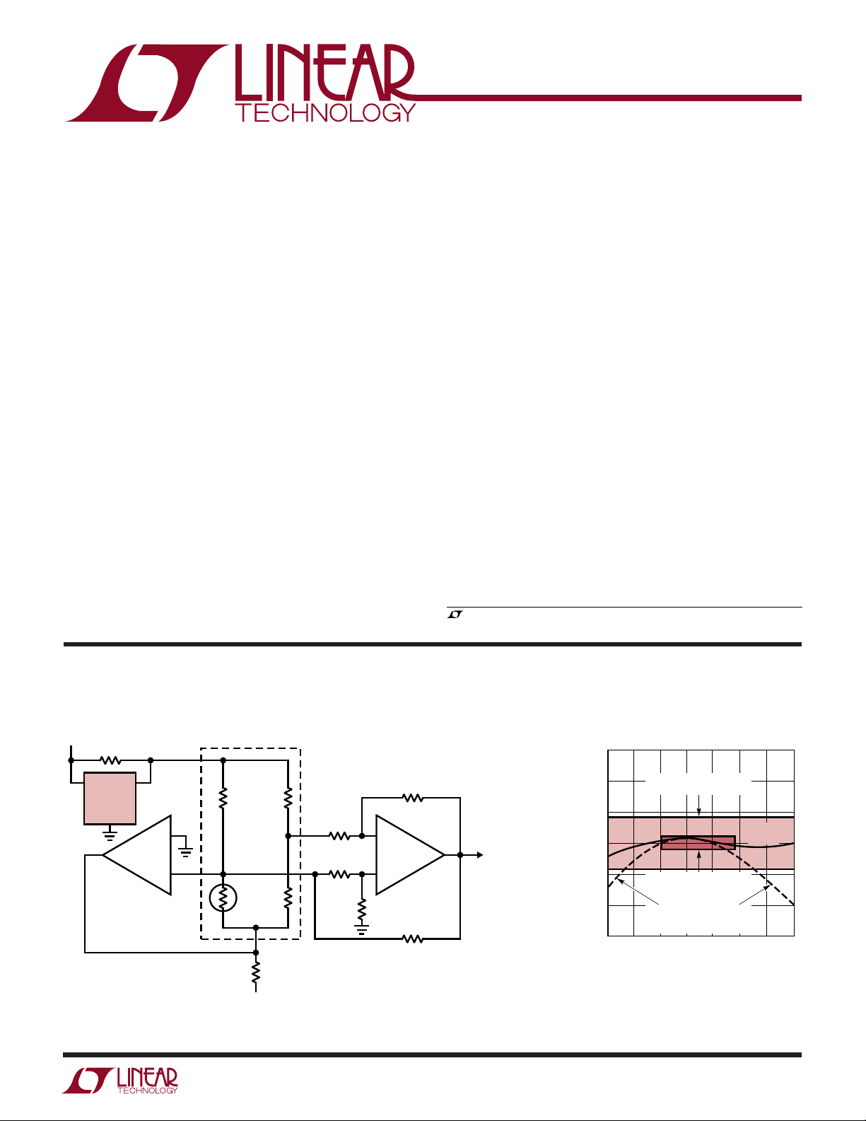
TEMPERATURE (˚C)
–50
OUTPUT VOLTAGE (NORMALIZED) (V)
1.001
1.002
1.003
25 75
1019 TA02
1.000
0.999
–25 0
50 100 125
0.998
0.997
5ppm/°C
0°C TO 70°C “BOX”
LT1019
CURVE
UNCOMPENSATED
“STANDARD” BANDGAP
DRIFT CURVE
10ppm/°C
FULL TEMP RANGE “BOX”
LT1019
Precision Reference
U
DESCRIPTIO
■
Tight Initial Output Voltage: <0.05%
■
Ultralow Drift: 3ppm/°C Typical
■
Series or Shunt Operation
■
Curvature Corrected
■
Ultrahigh Line Rejection: ≈0.5ppm/V
■
Low Output Impedance: ≈0.02Ω
■
Plug-In Replacement for Present References
■
Available at 2.5V, 4.5V, 5V, and 10V
■
100% Noise Tested
■
Temperature Output
■
Industrial Temperature Range in SO-8
U
APPLICATIO S
■
Negative Shunt References
■
A/D and D/A Converters
■
Precision Regulators
■
Constant Current Sources
■
V/F Converters
■
Bridge Excitation
The LT®1019 is a third generation bandgap voltage reference utilizing thin film technology and a greatly improved
curvature correction technique. Wafer level trimming of
both reference and output voltage combines to produce
units with high yields to very low TC and tight initial
tolerance of output voltage.
The LT1019 can both sink and source up to 10mA and can
be used in either the series or shunt mode. This allows the
reference to be used for both positive and negative output
voltages without external components. Minimum input/
output voltage is less than 1V in the series mode, providing
improved tolerance of low line conditions.
The LT1019 is available in four voltages: 2.5V, 4.5V, 5V
and 10V. It is a direct replacement for most bandgap
references presently available including AD580, AD581,
REF-01, REF-02, MC1400, MC1404 and LM168.
, LTC and LT are registered trademarks of Linear Technology Corporation.
TYPICAL APPLICATION
15V
357Ω*
0.5W
IN
LT1019-5
GND
5V
OUT
†
A1
LT1637
Ultralinear Strain Guage
350Ω
BRIDGE
+
–
ACTIVE
ELEMENT
–15V
–5V
357Ω*
0.5W
U
R3
2M
R2
20k
R4
20k
*
REDUCES REFERENCE AND AMPLIFIER
LOADING TO ≈0.
**
IF R6 = R3, BRIDGE IS NOT LOADED BY R2 AND R4.
†
A1 V
ACTS AS A DIFFERENTIAL AMPLIFIER.
–
A2
LT1001
+
R5
2M
R6**
2M
LT1019 • TA01
AND DRIFT ARE NOT CRITICAL BECAUSE A2
OS
Output Voltage Drift
GAIN = 100
1
Page 2
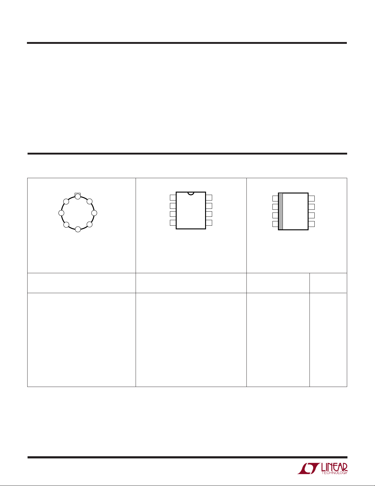
LT1019
TOP VIEW
S8 PACKAGE
8-LEAD PLASTIC SO
1
2
3
4
8
7
6
5
DNC*
INPUT
TEMP
GND
DNC*
DNC*
OUTPUT
TRIM
*INTERNALLY CONNECTED. DO NOT
CONNECT EXTERNALLY.
A
W
O
LUTEXI TIS
S
A
WUW
U
ARB
G
(Note 1)
Input Voltage .......................................................... 40V
Output Voltage (Note 2)
LT1019-5, LT1019-10 ........................................ 16V
LT1019-2.5, LT1019-4.5 ...................................... 7V
Output Short-Circuit Duration (Note 2)
VIN < 20V.................................................... Indefinite
20V ≤ VIN ≤ 35V ............................................. 10 sec
WU
/
PACKAGE
DNC*
INPUT
TEMP
8-LEAD TO-5 METAL CAN
*INTERNALLY CONNECTED. DO NOT
CONNECT EXTERNALLY
T
= 150°C, θ
JMAX
O
RDER I FOR ATIO
TOP VIEW
DNC*
8
1
2
3
4
GND (CASE)
H PACKAGE
= 150°C/ W, θJC = 45°C/W
JA
DNC*
7
DNC*
6
OUTPUT
5
TRIM
1
INPUT
2
TEMP
3
GND
4
*INTERNALLY CONNECTED. DO NOT
CONNECT EXTERNALLY.
T
= 100°C, θ
JMAX
Specified Temperature Range
Commercial .............................................0°C to 70°C
Industrial ............................................ –40°C to 85°C
Military ............................................. –55°C to 125°C
Trim Pin Voltage................................................... ±30V
Temp Pin Voltage ..................................................... 5V
Storage Temperature Range (Note 11) –65°C to 150°C
Lead Temperature (Soldering, 10 sec)................. 300°C
U
TOP VIEW
DNC*
8
DNC*
7
OUTPUT
6
TRIM
5
N8 PACKAGE
8-LEAD PDIP
T
= 130°C/ W
JA
JMAX
= 100°C, θ
= 130°C/ W
JA
LT1019ACH-2.5
LT1019ACH-4.5
LT1019ACH-5
LT1019ACH-10
LT1019AMH-2.5
LT1019AMH-4.5
LT1019AMH-5
LT1019AMH-10
ORDER PART
NUMBER
LT1019CH-2.5
LT1019CH-4.5
LT1019CH-5
LT1019CH-10
LT1019MH-2.5
LT1019MH-4.5
LT1019MH-5
LT1019MH-10
ORDER PART
NUMBER
LT1019ACN8-2.5
LT1019ACN8-4.5
LT1019ACN8-5
LT1019ACN8-10
LT1019CN8-2.5
LT1019CN8-4.5
LT1019CN8-5
LT1019CN8-10
LT1019IN8-2.5
LT1019IN8-4.5
LT1019IN8-5
LT1019IN8-10
ORDER PART
NUMBER
LT1019ACS8-2.5
LT1019ACS8-5
LT1019AIS8-2.5
LT1019AIS8-5
LT1019CS8-2.5
LT1019CS8-4.5
LT1019CS8-5
LT1019CS8-10
LT1019IS8-2.5
LT1019IS8-5
S8 PART
MARKING
19A25
19A05
19AI2
19AI5
1925
1945
1905
1910
19I25
19I05
2
Page 3
U
AVAILABLE OPTIO S
LT1019
OUTPUT TEMPERATURE
VOLTAGE TEMPERATURE ACCURACY COEFFICIENT TO-5 SO-8 PDIP-8
(V) (
2.5 0 to 70 0.05 5 LT1019ACH-2.5 LT1019ACS8-2.5 LT1019ACN8-2.5
4.5 0 to 70 0.05 5 LT1019ACH-4.5 LT1019ACN8-4.5
5 0 to 70 0.05 5 LT1019ACH-5 LT1019ACS8-5 LT1019ACN8-5
10 0 to 70 0.05 5 LT1019ACH-10 LT1019ACN8-10
°
C) (%) (ppm/°C) H8 S8 N8
0.2 20 LT1019CH-2.5 LT1019CS8-2.5 LT1019CN8-2.5
–40 to 85 0.05 10 LT1019AIS8-2.5
0.2 20 LT1019IS8-2.5 LT1019IN8-2.5
–55 to 125 0.05 10 LT1019AMH-2.5
0.2 25 LT1019MH-2.5
0.2 20 LT1019CH-4.5 LT1019CS8-4.5 LT1019CN8-4.5
–40 to 85 0.2 20 LT1019IN8-4.5
–55 to 125 0.05 10 LT1019AMH-4.5
0.2 25 LT1019MH-4.5
0.2 20 LT1019CH-5 LT1019CS8-5 LT1019CN8-5
–40 to 85 0.05 10 LT1019AIS8-5
0.2 20 LT1019IS8-5 LT1019IN8-5
–55 to 125 0.05 10 LT1019AMH-5
0.2 25 LT1019MH-5
0.2 20 LT1019CH-10 LT1019CS8-10 LT1019CN8-10
–40 to 85 0.2 20 LT1019IN8-10
–55 to 125 0.05 10 LT1019AMH-10
0.2 25 LT1019MH-10
PACKAGE TYPE
LECTRICAL C CHARA TERIST
E
The ● denotes specifications which apply over the full operating temperature range, otherwise specifications are TA = 25°C.
VIN = 15V, I
SYMBOL PARAMETER CONDITIONS MIN TYP MAX MIN TYP MAX UNITS
TC Output Voltage LT1019C (0°C to 70°C) ● 3 5 5 20 ppm/°C
∆V
OUT
∆V
IN
RR Ripple Rejection 50Hz ≤ f ≤ 400Hz 90 110 90 110 dB
= 0 unless otherwise noted.
OUT
Output Voltage Tolerance 0.02 0.05 0.02 0.2 %
Temperature Coefficient LT1019I (–40°C to 85°C)
(Note 3) LT1019M (–55°C to 125°C)
Line Regulation (Note 4) (V
OUT
ICS
LT1019A LT1019
● 3 10 5 20 ppm/°C
● 5 10 8 25 ppm/°C
+ 1.5V) ≤ VIN ≤ 40V 0.5 3 0.5 3 ppm/V
● 1.0 5 1.0 5 ppm/V
● 84 84 dB
3
Page 4
LT1019
LECTRICAL C CHARA TERIST
E
The ● denotes specifications which apply over the full operating temperature range, otherwise specifications are TA = 25°C.
VIN = 15V, I
SYMBOL PARAMETER CONDITIONS MIN TYP MAX MIN TYP MAX UNITS
∆V
OUT
∆I
OUT
I
Q
I
SC
e
n
= 0 unless otherwise noted.
OUT
Load Regulation Series 0 ≤ I
Mode (Notes 4, 5) ● 0.08 0.08 mV/mA (Ω)
Load Regulation, 1mA ≤ I
Shunt Mode 2.5V, 4.5V, 5V
Thermal Regulation (Note 7) ∆P = 200mW, t = 50ms 0.1 0.5 0.1 0.5 ppm/mW
Quiescent Current 0.65 1.0 0.65 1.2 mA
Series Mode
Minimum Shunt Current (Note 8) ● 0.5 0.8 0.5 0.8 mA
Minimum Input/Output I
Voltage Differential I
Trim Range LT1019-2.5 ±3.5 ±6 ±3.5 ±6%
Short-Circuit Current 2V ≤ VIN ≤ 35V 15 25 50 15 25 50 mA
Output Connected to GND
Output Voltage Noise 10Hz ≤ f ≤ 1kHz 2.5 4 2.5 4 ppm (RMS)
(Note 10) 0.1Hz ≤ f ≤ 10Hz 2.5 2.5 ppm (P-P)
OUT
10V
≤ 1mA ● 0.9 1.1 0.9 1.1 V
OUT
= 10mA ● 1.3 1.3 V
OUT
LT1019-5 ±3.5 5, –13 ±3.5 5, –13 %
LT1019-10 ±3.5 5, –27 ±3.5 5, –27 %
ICS
LTC1019A LTC1019
≤ 10mA (Note 5) 0.02 0.05 0.02 0.05 mV/mA (Ω)
≤ 10mA (Notes 5, 6)
SHUNT
● 0.1 0.4 0.1 0.4 mV/mA (Ω)
● 0.8 0.8 mV/mA (Ω)
● 1.3 1.5 mA
● 10 10 mA
Note 1: Absolute Maximum Ratings are those values beyond which the life
of a device may be impaired.
Note 2: These are high power conditions and are therefore guaranteed
only at temperatures equal to or below 70°C. Input is either floating, tied to
output or held higher than output.
Note 3: Output voltage drift is measured using the box method. Output
voltage is recorded at T
readings is subtracted from the highest and the resultant difference is
divided by (T
Note 4: Line regulation and load regulation are measured on a pulse basis
with low duty cycle. Effects due to die heating must be taken into account
separately. See thermal regulation and application section.
Note 5: Load regulation is measured at a point 1/8" below the base of the
package with Kelvin contacts.
Note 6: Shunt regulation is measured with the input floating. This
parameter is also guaranteed with the input connected (V
0mA ≤ I
– T
MAX
≤ 10mA. Shunt and sink current flow into the output.
SINK
MIN
MIN
).
, 25°C and T
. The lowest of these three
MAX
– V
IN
OUT
) > 1V,
Note 7: Thermal regulation is caused by die temperature gradients created
by load current or input voltage changes. This effect must be added to
normal line or load regulation.
Note 8: Minimum shunt current is measured with shunt voltage held
20mV below the value measured at 1mA shunt current.
Note 9: Minimum input/output voltage is measured by holding input
voltage 0.5V above the nominal output voltage, while measuring
– V
OUT
.
V
IN
Note 10: RMS noise is measured with a single pole highpass filter at 10Hz
and a 2-pole lowpass filter at 1kHz. The resulting output is full-wave
rectified and then integrated for a fixed period, making the final reading an
average as opposed to RMS. A correction factor of 1.1 is used to convert
from average to RMS, and a second correction of 0.88 is used to correct
the nonideal bandpass of the filters.
Note 11: If the part is stored outside of the specified temperature range,
the output may shift due to hysteresis.
4
Page 5

LPER
INPUT VOLTAGE (V)
0
CURRENT (mA)
0.8
1.0
1.2
40
LT1019 • TPC03
0.6
0.4
0
10
20
30
0.2
1.6
1.4
35
5
15
25
45
125°C
25°C
–55°C
F
O
Quiescent Current (LT1019-2.5)
1.6
1.4
1.2
1.0
0.8
0.6
CURRENT (mA)
0.4
0.2
0
0
5
10
15
20
25
INPUT VOLTAGE (V)
Minimum Input/Output Voltage
Differential
10
7.5
5.0
OUTPUT CURRENT (mA)
2.5
0
0.2 0.6
0.4
0
INPUT/OUTPUT VOLTAGE (V)
TJ = –55°CTJ = 125°C
1.0 1.8
1.2
0.8
R
125°C
25°C
–55°C
35
30
LT1019 • TPC01
TJ = 25°C
1.4
LT1019 • TPC04
ATYPICA
40
1.6
UW
CCHARA TERIST
E
C
Quiescent Current
(LT1019-4.5/LT1019-5)
1.6
1.4
1.2
1.0
0.8
0.6
CURRENT (mA)
0.4
0.2
45
0
0
5
Load Regulation
2.0
TJ = 25°C
1.5
1.0
0.5
LT1019-2.5
0
–0.5
OUTPUT CHANGE (mV)
–1.0
–1.5
–2.0
–8
–10
ICS
125°C
25°C
–55°C
15
20
10
INPUT VOLTAGE (V)
LT1019-10
LT1019-4.5/LT1019-5
–6
SINKING SOURCING
OUTPUT CURENT (mA)
–4
–2
0
35
25
30
LT1019 • TPC02
2
6
4
LT1019 • TPC05
LT1019
Quiescent Current (LT1019-10)
45
40
Ripple Rejection
120
110
100
90
80
70
60
50
INPUT VOLTAGE/OUTPUT VOLTAGE (dB)
10
8
40
10 1k 10k 1M
LT1019-2.5
100
LT1019-10
FREQUENCY (Hz)
TJ = 25°C
LT1019-4.5
LT1019-5
100k
LT1019 • TPC06
Shunt Mode Characteristics
(LT1019-2.5)
1.0
INPUT OPEN
0.9
0.8
0.7
0.6
0.5
0.4
CURRENT (mA)
0.3
TJ = 125°C
0.2
0.1
0
0
0.5 1.5
1.0
OUTPUT-TO-GROUND VOLTAGE (V)
TJ = 25°C
TJ = –55°C
2.0
2.5
3.0
3.5
LT1019 • TPC07
4.0
Shunt Mode Characteristics
(LT1019-5)
1.0
INPUT OPEN
0.9
0.8
0.7
0.6
0.5
0.4
CURRENT (mA)
0.3
TJ = 125°C
0.2
0.1
0
0
TJ = 25°C
TJ = –55°C
13
2
OUTPUT-TO-GROUND VOLTAGE (V)
4
Shunt Mode Characteristics
(LT1019-10)
1.0
INPUT OPEN
0.9
0.8
0.7
0.6
0.5
0.4
CURRENT (mA)
TJ = 125°C
0.3
0.2
0.1
7
6
5
8
LT1019 • TPC08
0
TJ = 25°C
TJ = –55°C
0
26
4
OUTPUT-TO-GROUND VOLTAGE (V)
8
14
12
10
16
LT1019 • TPC09
5
Page 6

LT1019
Temp Pin Voltage
0.90
0.85
0.80
0.75
0.70
0.65
0.60
VOLTAGE (V)
0.55
0.50
0.45
0.40
–50
–25
LPER
25
0
JUNCTION TEMPERATURE (°C)
R
F
O
50
75
ATYPICA
100
LT1019 • TPC10
UW
E
C
125
CCHARA TERIST
Line Regulation
140
I
OUT
120
TJ = 25°C
100
80
60
40
20
LT1019-2.5
0
–10
OUTPUT VOLTAGE CHANGE (µV)
–20
–30
0
515
10
20
INPUT VOLTAGE (V)
ICS
LT1019-10
LT1019-5
30
25
35
LT1019 • TPC11
LT1019-2.5* Stability with
Output Capacitance
10
1
REGION OF POSSIBLE
0.1
0.01
OUTPUT CAPACITOR (µF)
0.001
40
0.0001
20 0 10
*LT1019-4.5/LT1019-5/LT1019-10 ARE STABLE
10
15 5 5 15
SINK CURRENT SOURCE CURRENT
OUTPUT CURRENT (mA)
WITH ALL LOAD CAPACITANCE.
INSTABILITY
20
1019 G12
W
BLOCK DIAGRA
LT1019-2.5 = 11k
LT1019-4.5 = 13.9k
LT1019-5 = 16k
LT1019-10 = 37.1k
R3
80k
TRIM
LT1019-4.5, LT1019-5,
LT1019-10 = 5k
LT1019-2.5 = 10k
R2
1.188V
UU W U
APPLICATIO S I FOR ATIO
Line and Load Regulation
Line regulation on the LT1019 is nearly perfect. A 10V
change in input voltage causes a typical output shift of less
than 5ppm. Load regulation (sourcing current) is nearly as
good. A 5mA change in load current shifts output voltage
by only 100µV. These are
low duty cycle pulses to eliminate heating effects. In real
world applications, the
changes must be considered.
electrical
thermal
effects, measured with
effects of load and line
R1
V
IN
–
V
+
OUT
GND
LT1019 • BD
Two separate thermal effects are evident in monolithic
circuits. One is a gradient effect, where power dissipation
on the die creates temperature gradients. These gradients
can cause output voltage shifts
ture coefficient of the reference is zero
even if the overall tempera-
. The LT1019, unlike
previous references, specifies thermal regulation caused
by die temperature gradients.The specification is
0.5ppm/mW. To calculate the effect on output voltage,
simply multiply the
change
in device power dissipation by
6
Page 7

UU W U
APPLICATIO S I FOR ATIO
LT1019
the thermal regulation specification. Example: a 10V
device with a nominal input voltage of 15V and load
current of 5mA. Find the effect of an input voltage change
of 1V and a load current change of 2mA.
∆P (line change) = (∆VIN)(I
∆V
∆P (load change)= (∆I
∆V
Even though these effects are small, they should be taken
into account in critical applications, especially where input
voltage or load current is high.
The second thermal effect is overall die temperature
change. The magnitude of this change is the product of
change in power dissipation times the thermal resistance
(θJA) of the IC package ≅ (100°C/ W to 150°C/ W). The
effect on the reference output is calculated by multiplying
die temperature change by the temperature drift specification of the reference. Example: same conditions as above
with θJA = 150°C/W and an LT1019 with 20ppm/°C drift
specification.
∆P (line change) = 5mW
∆V
∆P (load change)= 10mW
∆V
These calculations show that thermally induced output
voltage variations can easily exceed the electrical effects.
In critical applications where shifts in power dissipation
are expected, a small clip-on heat sink can significantly
improve these effects by reducing overall die temperature
change. Alternately, an LT1019A can be used with four
times lower TC. If warm-up drift is of concern, these
measures will also help. With warm-up drift,
power dissipation must be considered. In the example
given, warm-up drift (worst case) is equal to:
= (0.5ppm/mW)(5mW) = 2.5ppm
OUT
LOAD
= (2mA)(5V) = 10mW
= (0.5ppm/mW)(10mW) = 5ppm
OUT
= (5mW)(150°C/W)(20ppm/°C)
OUT
= 15ppm
= (10mW)(150°C/W)(20ppm/°C)
OUT
= 30ppm
) = (1V)(5mA) = 5mW
LOAD
)(VIN – V
OUT
)
total
device
Warm-up drift = [(VIN)(IQ) + (VIN – V
[(θJA)(TC)]
with IQ (quiescent current) = 0.6mA,
Warm-up drift = [(15V)(0.6mA) + (5V)(5mA)]
[(150°C/W)(25ppm/°C)]
= 127.5ppm
Note that 74% of the warm-up drift is due to load current
times input/output differential. This emphasizes the
importance of keeping both these numbers low in critical
applications.
Note that line regulation is now affected by reference
output impedance. R1 should have a wattage rating high
enough to withstand full input voltage if output shorts
must be tolerated. Even with load currents below 10mA,
R1 can be used to reduce power dissipation in the LT1019
for lower warm-up drift, etc.
Output Trimming
Output voltage trimming on the LT1019 is nominally
accomplished with a potentiometer connected from output to ground with the wiper tied to the trim pin. The
LT1019 was made compatible with existing references, so
the trim range is large: + 6%, –6% for the LT1019-2.5,
+5%, –13% for the LT1019-5, and +5%, –27% for the
LT1019-10. This large trim range makes precision trimming rather difficult. One solution is to insert resistors in
series with both ends of the potentiometer. This has the
disadvantage of potentially poor tracking between the
fixed resistors and the potentiometer. A second method of
reducing trim range is to insert a resistor in series with the
wiper of the potentiometer. This works well only for very
small trim range because of the mismatch in TCs between
the series resistor and the internal thin film resistors.
These film resistors can have a TC as high as 500ppm/°C.
That same TC is then transferred to the change in output
voltage: a 1% shift in output voltage causes a
(500ppm)(1%) = 5ppm/°C change in output voltage drift.
OUT
)(I
LOAD
)]
7
Page 8

LT1019
UU W U
APPLICATIO S I FOR ATIO
The worst-case error in initial output voltage for the
LT1019 is 0.2%, so a series resistor is satisfactory if the
output is simply trimmed to nominal value. The maximum
TC shift expected would be 1ppm/°C.
Using the Temp Pin
The LT1019 has a TEMP pin like several other bandgap
references. The voltage on this pin is directly proportional to absolute temperature (PTAT) with a slope of
approximately 2.1mV/°C. Room temperature voltage is
therefore approximately (295°K)(2.1mV/°C) = 620mV.
This voltage varies with process parameters and should
not be used to measure absolute temperature, but
rather relative temperature changes. Previous bandgap
references have been very sensitive to any loading on
the TEMP pin because it is an integral part of the
reference “core” itself. The LT1019 “taps” the core at a
special point which has much less effect on the reference. The relationship between TEMP pin loading and
a change in reference output voltage is less than
0.05%/µA, about ten times improvement over previous
references.
capacitance and load. The 2.5V device can oscillate when
sinking currents between 1mA and 6mA for load capacitance between 400pF and 2µF (see Figure 1).
If output bypassing is desired to reduce high frequency
output impedance, keep in mind that loop phase margin is
significantly reduced for output capacitors between 500pF
and 1µF if the capacitor has low ESR (Effective Series
Resistance). This can make the output “ring” with tran-
V
IN
LT1019
2Ω TO 5Ω
+
2µF
TANTALUM
(a) (b)
Figure 1. Output Bypassing
V
IN
LT1019
2Ω TO 5Ω
+
2µF TO 10µF
TANTALUM
1019 F01
sient loads. The best transient load response is obtained
by deliberately adding a resistor to increase ESR as shown
in Figure 1.
Output Bypassing
The LT1019 is designed to be stable with a wide range of
load currents and output capacitors. The 4.5V, 5V, and
10V devices do not oscillate under any combination of
U
TYPICAL APPLICATIO S
Wide Range Trim ≥ ±5%
R1
25k
V
OUT
1019 TA03
OUT
IN
V
IN
LT1019
TRIM
GND
Use configuration (a) if DC voltage error cannot be compromised as load current changes. Use (b) if absolute
minimum peak perturbation at the load is needed. For best
transient response, the output can be loaded with ≥1mA
DC current.
Narrow Trim Range (±0.2%)
R1
100k
1019 TA05
V
OUT
OUT
V
IN
IN
LT1019
TRIM
GND
*INCREASE TO 4.7M FOR LT1019A (±0.05%)
R2*
1.5M
8
Page 9

U
TYPICAL APPLICATIO S
LT1019
Trimming LT1019-5 Output to 5.120V
OUT
IN
V
IN
LT1019-5
TRIM
GND
*LOW TC CERMET
Precision 1µA Current Source
15V
11.5k
1%
5k*
8.25k
1%
OUT
IN
LT1019-2.5
TRIM
GND
V
OUT
41.2k
1%
5k*
±1% TRIM
4.02k
1%
1019 TA04
Trimming LT1019-10 Output to 10.240V
V
OUT
V
IN
OUT
IN
LT1019-10
TRIM
GND
*LOW TC CERMET
90.9k
1%
5k*
±1% TRIM
4.02k
1%
1019 TA06
Negative Series Reference
+
V
LT1019
R1*
IN
OUT
D1*
R2*
GND
I
Z
OUT
= 1µA
OUT
≥ 1011Ω
2.49M
1%
–
LT1012
+
*LOW TC CERMET, TRIM RANGE = ±1.5%
Output Current Boost with Current Limit
V+ ≥ (V
OUT
+ 2.8V)
LED
V
OUT
±11V COMPLIANCE
1019 TA07
GLOWS IN
CURRENT LIMIT
(DO NOT OMIT)
IN
LT1019
GND
R1
220Ω
OUT
IN
V
*R1 =
8.2Ω
2N2905
≤ 100mA
I
LOAD
2µF SOLID TANTALUM
2N2905
+
– 5V
2mA
Q1
, R2 =
1019 TA08
AT 50mA–V
–V
REF
–
– V
V
REF
1mA
, D1 = V
REF
+ 5V
1019 TA10
9
Page 10

LT1019
WW
SCHE ATIC DIAGRA
IN
V
R21
20Ω
R32
Q32
Q31
Q33
R20
500Ω
750Ω
R23
Q27
100Ω
Q28
Q29
Q26
Q20
Q30
R33
R24
Q25
850Ω
OUT
V
1k
R17
R34
R27
R28
R26
R13
GND
24.5k
R19
15Ω
R31
22k
Q34
Q35
R16
3k
500Ω
4k
R15
3k
9k
9k
3k
Q23
Q19
Q18
Q6B
Q5 Q6A
Q24
Q21
C4
R35
C3
27k
Q16
Q15
Q17
Q14
Q22
Q13
Q11 Q12
2k
R18
Q10
1k
Q9
Q8
R12
R42
7.2k
4k
10
R25
Q7
Q37
R39
Q36
R36
82k
Q38
2.5
R5
R4
R14
R2
72k
R6
R29
Q2
780Ω
Q1
80k
TRIM
1k
R1
Q4
SHORT
FOR
Q3
R9
3k
1.6k
R8
2.5k
R7
R11A
R38
1.9k
3.75k
R11B
R37
5k
R3
1k
2k
Page 11
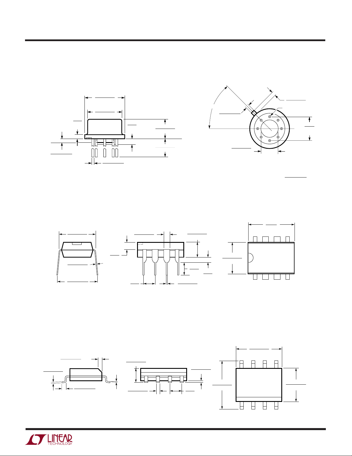
PACKAGE DESCRIPTIO
LT1019
U
Dimensions in inches (millimeters) unless otherwise noted.
H Package
8-Lead TO-5 Metal Can (0.200 PCD)
(LTC DWG # 05-08-1320)
SEATING
PLANE
0.335 – 0.370
(8.509 – 9.398)
DIA
0.305 – 0.335
(7.747 – 8.509)
0.016 – 0.021**
(0.406 – 0.533)
0.050
(1.270)
MAX
GAUGE
PLANE
(12.700 – 19.050)
0.010 – 0.045*
(0.254 – 1.143)
0.040
(1.016)
MAX
8-Lead PDIP (Narrow 0.300)
(LTC DWG # 05-08-1510)
0.300 – 0.325
(7.620 – 8.255)
0.065
(1.651)
0.009 – 0.015
(0.229 – 0.381)
+0.035
0.325
–0.015
+0.889
8.255
()
–0.381
*THESE DIMENSIONS DO NOT INCLUDE MOLD FLASH OR PROTRUSIONS.
MOLD FLASH OR PROTRUSIONS SHALL NOT EXCEED 0.010 INCH (0.254mm)
TYP
0.045 – 0.065
(1.143 – 1.651)
0.100
(2.54)
BSC
0.165 – 0.185
(4.191 – 4.699)
0.500 – 0.750
N8 Package
REFERENCE
PLANE
0.130 ± 0.005
(3.302 ± 0.127)
0.125
(3.175)
MIN
0.018 ± 0.003
(0.457 ± 0.076)
0.027 – 0.045
MAX
(0.686 – 1.143)
PIN 1
(0.406 – 0.610)
3
0.016 – 0.024
H8(TO-5) 0.200 PCD 1197
5
4
N8 1098
°TYP
45
0.028 – 0.034
(0.711 – 0.864)
0.110 – 0.160
(2.794 – 4.064)
INSULATING
STANDOFF
*
LEAD DIAMETER IS UNCONTROLLED BETWEEN THE REFERENCE PLANE
AND 0.045" BELOW THE REFERENCE PLANE
**
FOR SOLDER DIP LEAD FINISH, LEAD DIAMETER IS
0.400*
(10.160)
876
0.255 ± 0.015*
(6.477 ± 0.381)
0.020
(0.508)
MIN
12
0.200
(5.080)
TYP
8-Lead Plastic Small Outline (Narrow 0.150)
0.010 – 0.020
(0.254 – 0.508)
0.008 – 0.010
(0.203 – 0.254)
*
DIMENSION DOES NOT INCLUDE MOLD FLASH. MOLD FLASH
SHALL NOT EXCEED 0.006" (0.152mm) PER SIDE
**
DIMENSION DOES NOT INCLUDE INTERLEAD FLASH. INTERLEAD
FLASH SHALL NOT EXCEED 0.010" (0.254mm) PER SIDE
× 45°
0.016 – 0.050
(0.406 – 1.270)
0.053 – 0.069
(1.346 – 1.752)
0°– 8° TYP
0.014 – 0.019
(0.355 – 0.483)
I
nformation furnished by Linear Technology Corporation is believed to be accurate and reliable.
However, no responsibility is assumed for its use. Linear Technology Corporation makes no representation that the interconnection of its circuits as described herein will not infringe on existing patent rights.
S8 Package
(LTC DWG # 05-08-1610)
TYP
0.004 – 0.010
(0.101 – 0.254)
0.050
(1.270)
BSC
0.228 – 0.244
(5.791 – 6.197)
0.189 – 0.197*
(4.801 – 5.004)
7
8
1
2
5
6
0.150 – 0.157**
(3.810 – 3.988)
3
4
SO8 1298
11
Page 12

LT1019
TYPICAL APPLICATION
U
Negative 10V Reference for CMOS DAC
OUT
LT1019-10
TRIM
GND
1.2k
–15V
59k
1%
5k*
5.76k
1%
*LOW TC CERMET, TRIM RANGE = ±1.5%
LTC1595
REF
FB
I
OUT
30pF
–
LT1007
+
V
1019 TA09
OUT
RELATED PARTS
PART NUMBER DESCRIPTION COMMENTS
LT1027 Precision 5V Reference Lowest TC, High Accuracy, Low Noise, Zener Based
LT1236 Precision Reference 5V and 10V Zener Based, 5ppm/°C, SO-8 Package
LT1460 Micropower Precision Series Reference Bandgap, 130µA Supply Current, 10ppm/°C, Available in SOT-23 Package
LT1634 Micropower Precision Shunt Reference Bandgap 0.05%, 10ppm/°C, 10µA Supply Current
LTC1798 Micropower Low Dropout Reference 0.15% Max, 6.5µA Supply Current
LT1461 Micropower Low Dropout Reference 3ppm/°C, 0.04%, 50µA Supply Current
1019fc LT/TP 1299 2K REV C • PRINTED IN USA
LINEAR TECHNOLOGY CORPORATION 1993
12
Linear Technology Corporation
1630 McCarthy Blvd., Milpitas, CA 95035-7417
(408) 432-1900 ● FAX: (408) 434-0507
●
www.linear-tech.com
 Loading...