

Page 1
Linear Integrated Systems
• 4042 Clipper Court • Fremont, CA 94538 • Tel: 510 490-9160 • Fax: 510 353-0261
Doc 201151 05/14/2014 Rev#A30 ECN# LSK489
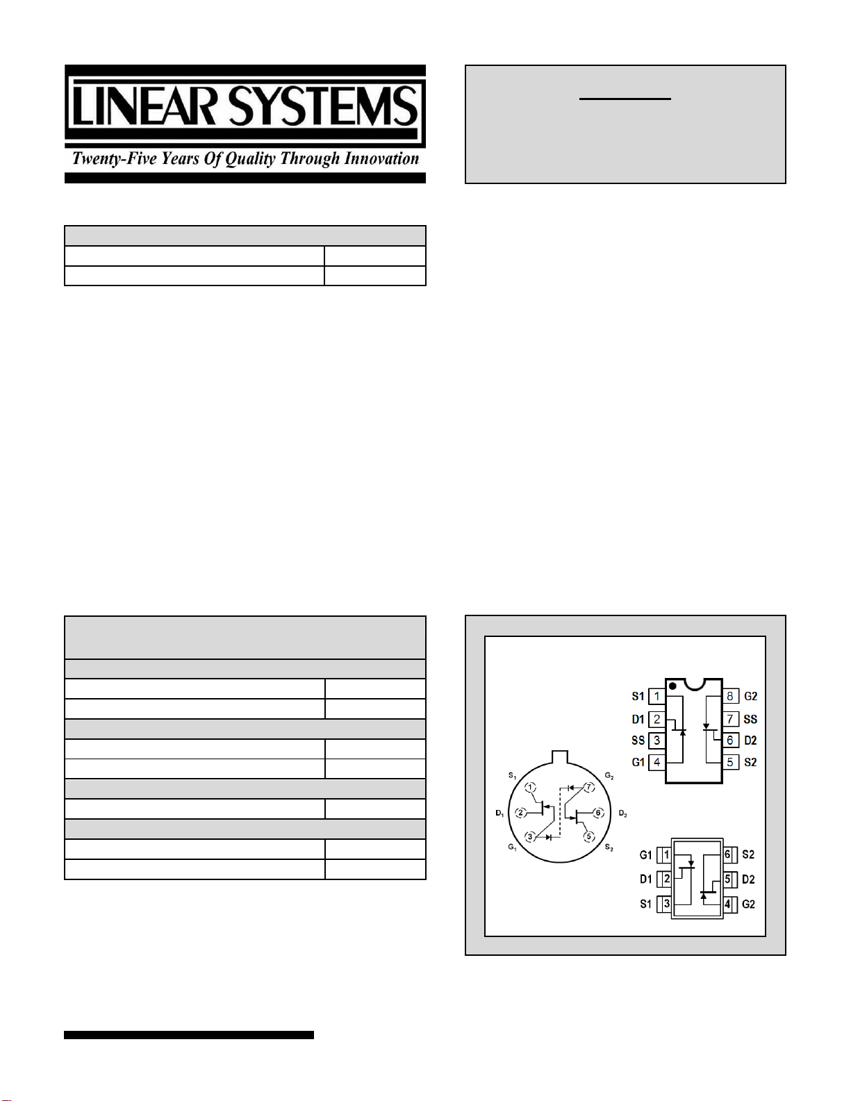
FEATURES
ULTRA LOW NOISE
en = 1.8nV/√Hz
LOW INPUT CAPACITANCE
Ciss = 4pF
ABSOLUTE MAXIMUM RATINGS1
@ 25 °C (unless otherwise stated)
Maximum Temperatures
Storage Temperature
-55 to +150°C
Junction Operating Temperature
-55 to +150°C
Maximum Power Dissipation, TA = 25°C
Continuous Power Dissipation, per side 4
300mW
Power Dissipation, total 5
500mW
Maximum Currents
Gate Forward Current
I
G(F)
= 10mA
Maximum Voltages
Gate to Source
V
GSO
= 60V
Gate to Drain
V
GDO
= 60V
Features
Reduced Noise due
to process improvement
Monolithic Design
High slew rate
Low offset/drift voltage
Low gate leakage lgss & lg
High CMRR 102 dB
Benefits
Tight differential voltage match vs.
current
Improved op amp speed settling time
accuracy
Minimum Input Error trimming error
voltage
Lower intermodulation distortion
Applications
Wide band differential Amps
High speed temperature
compensated single ended input
amplifier amps
High speed comparators
Impedance Converters
Description
The LSK 489 series of high performance monolithic dual JFETs features extremely low noise, tight offset voltage and low drift
over temperature specifications, and is targeted for use in a wide range or precision instrumentation applications. This series has
a wide selection of offset and drift specifications. The SST series SO-8 package provided ease of manufacturing and the
symmetrical pinout prevents improper orientation. The SO-8 package is available with tape and reel options for compatibility with
automatic assembly methods. (See packaging data)
LSK489
LOW NOISE LOW CAPACITANCE
MONOLITHIC DUAL
N-CHANNEL JFET AMPLIFIER
TO-71
TOP VIEW
SOIC-A
SOT-23
TOP VIEW
* For equivalent single version, see LSK189
•
Page 2
Linear Integrated Systems
• 4042 Clipper Court • Fremont, CA 94538 • Tel: 510 490-9160 • Fax: 510 353-0261
Doc 201151 05/14/2014 Rev#A30 ECN# LSK489
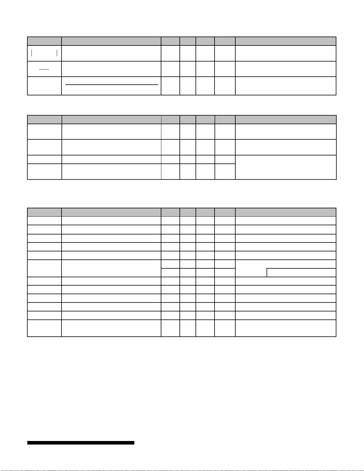
MATCHING CHARACTERISTICS @ 25°C (unless otherwise stated)
SYMBOL
CHARACTERISTIC
MIN
TYP
MAX
UNITS
CONDITIONS
GS2GS1 VV
Differential Gate to Source Cutoff
Voltage
20 mV
VDS = 10V, ID = 1mA
DSS2
DSS1
I
I
Gate to Source Saturation Current Ratio
0.9 1.0 VDS = 10V, V
GS
= 0V
CMRR
COMMON MODE REJECTION RATIO
-20 log│∆V
GS1-2
/∆VDS│
95
102 dB
VDS = 10V to 20V, ID = 200µA
SYMBOL
CHARACTERISTIC
MIN
TYP
MAX
UNITS
CONDITIONS
en
Noise Voltage
1.8
2.0
nV/√Hz
VDS = 15V, ID = 2.0mA, f = 1kHz,
NBW = 1Hz
en
Noise Voltage
2.8
3.5
nV/√Hz
VDS = 15V, ID = 2.0mA, f = 10Hz,
NBW = 1Hz
C
ISS
Common Source Input Capacitance
4 8
pF
VDS = 15V, ID = 500µA, f = 1MHz
C
RSS
Common Source Reverse Transfer
Capacitance
3
pF
ELECTRICAL CHARACTERISTICS @ 25°C (unless otherwise stated)
SYMBOL
CHARACTERISTIC
MIN
TYP
MAX
UNITS
CONDITIONS
BV
GSS
Gate to Source Breakdown Voltage
-60 V VDS = 0, ID = -1nA
V
(BR)G1 - G2
Gate to Gate Breakdown Voltage
±30
±45 V
IG= ±1µA, ID=IS=0 A (Open Circuit)
V
GS(OFF)
Gate to Source Pinch-off Voltage
-1.5 -3.5 V VDS = 15V, ID = 1nA
VGS
Gate to Source Operating Voltage
-0.5 -3.5 V VDS = 15V, ID = 500µA
I
DSS
2
Drain to Source Saturation Current
2.5 5 15
mA
VDG = 15V, V
GS
= 0
IG
Gate Operating Current
-2
-25
pA
VDG = 15V, ID = 200µA
-0.8
-10
nA TA = 125°C
I
GSS
Gate to Source Leakage Current
-100
pA
VDG = -15V, V
DS
= 0
Gfs
Full Conductance Transconductance
1500
µS
VDG = 15V, V
GS
= 0, f = 1kHz
Gfs
Transconductance
1000
1500 µS
VDG = 15V, ID = 500µA
GOS
Full Output Conductance
40
µS
VDG = 15V, V
GS
= 0
GOS
Output Conductance
1.8
2.7
µS
VDG = 15V, ID = 200µA
NF
Noise Figure
0.5
dB
VDS = 15V, V
GS
= 0, RG = 10MΩ,
f = 100Hz, NBW = 6Hz
Page 3
Linear Integrated Systems
• 4042 Clipper Court • Fremont, CA 94538 • Tel: 510 490-9160 • Fax: 510 353-0261
Doc 201151 05/14/2014 Rev#A30 ECN# LSK489
NOTES
1. Absolute maximum ratings are limiting values above which serviceability may be impaired.
2. Pulse width ≤2ms.
3. All MIN/TYP/MAX Limits are absolute values. Negative signs indicate electrical polarity only.
4. Derate 2.4 mW/°C above 25°C.
5. Derate 4 mW/°C above 25°C.
Information furnished by Linear Integrated Systems is believed to be accurate and reliable. However, no responsibility is assumed for its
use; nor for any infringement of patents or other rights of third parties which may result from its use. No license is granted by implication or
otherwise under any patent or patent rights of Linear Integrated Systems.
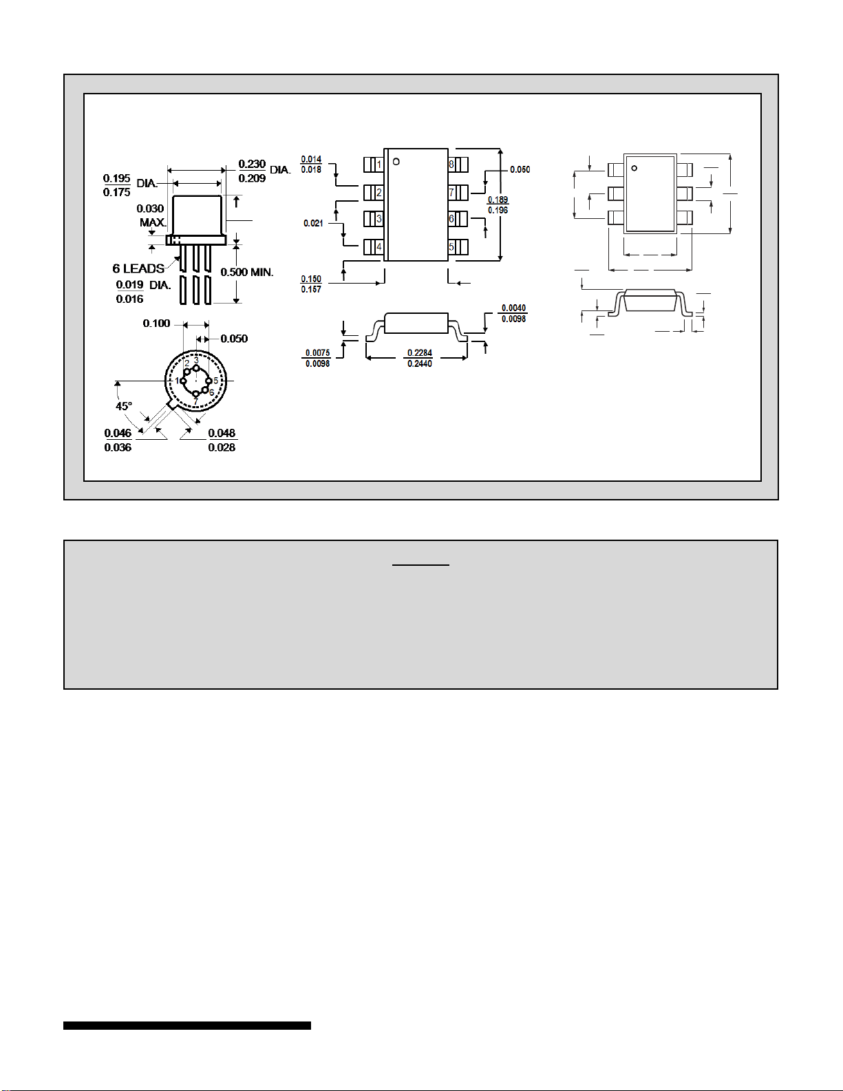
PACKAGE DIMENSIONS
DIMENSIONS IN INCHES
1
3
5
SOT-23
DIMENSIONS IN
MILLIMETERS
2
4
6
0.95
1.90
1.50
1.75
2.60
3.00
0.35
0.50
2.80
3.00
0.90
1.30
0.00
0.15
0.09
0.20
0.10
0.60
Six Lead
0.210
0.170
DIMENSIONS IN INCHES
DIMENSIONS IN MILLIMETERS
TO-71
SIX LEAD
SOIC-A
SOT-23
SIX LEAD
Page 4
Linear Integrated Systems
• 4042 Clipper Court • Fremont, CA 94538 • Tel: 510 490-9160 • Fax: 510 353-0261
Doc 201151 05/14/2014 Rev#A30 ECN# LSK489
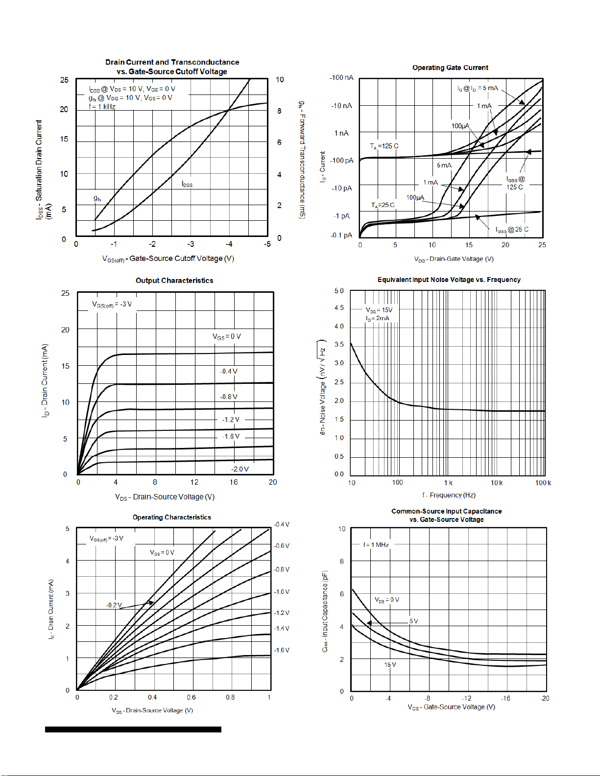
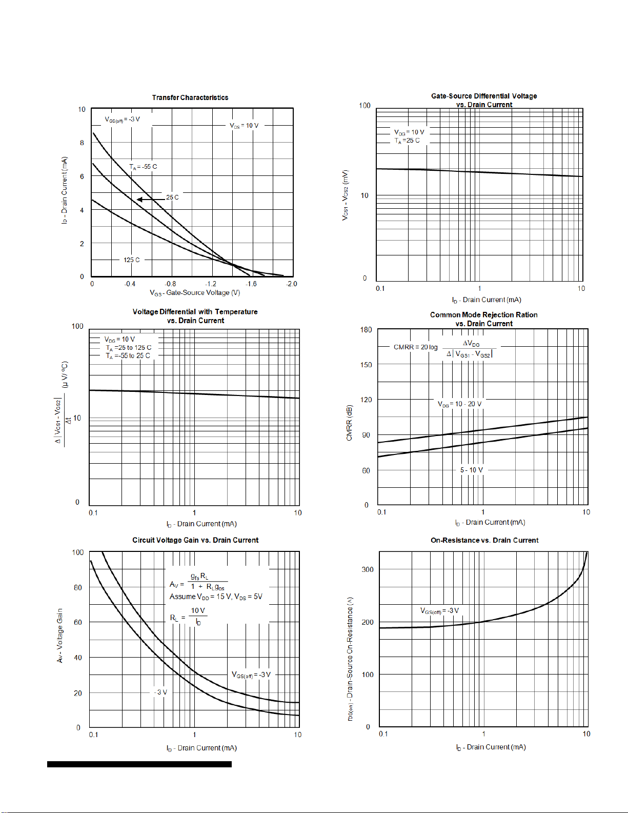
Typical Characteristics
Page 5
Linear Integrated Systems
• 4042 Clipper Court • Fremont, CA 94538 • Tel: 510 490-9160 • Fax: 510 353-0261
Doc 201151 05/14/2014 Rev#A30 ECN# LSK489
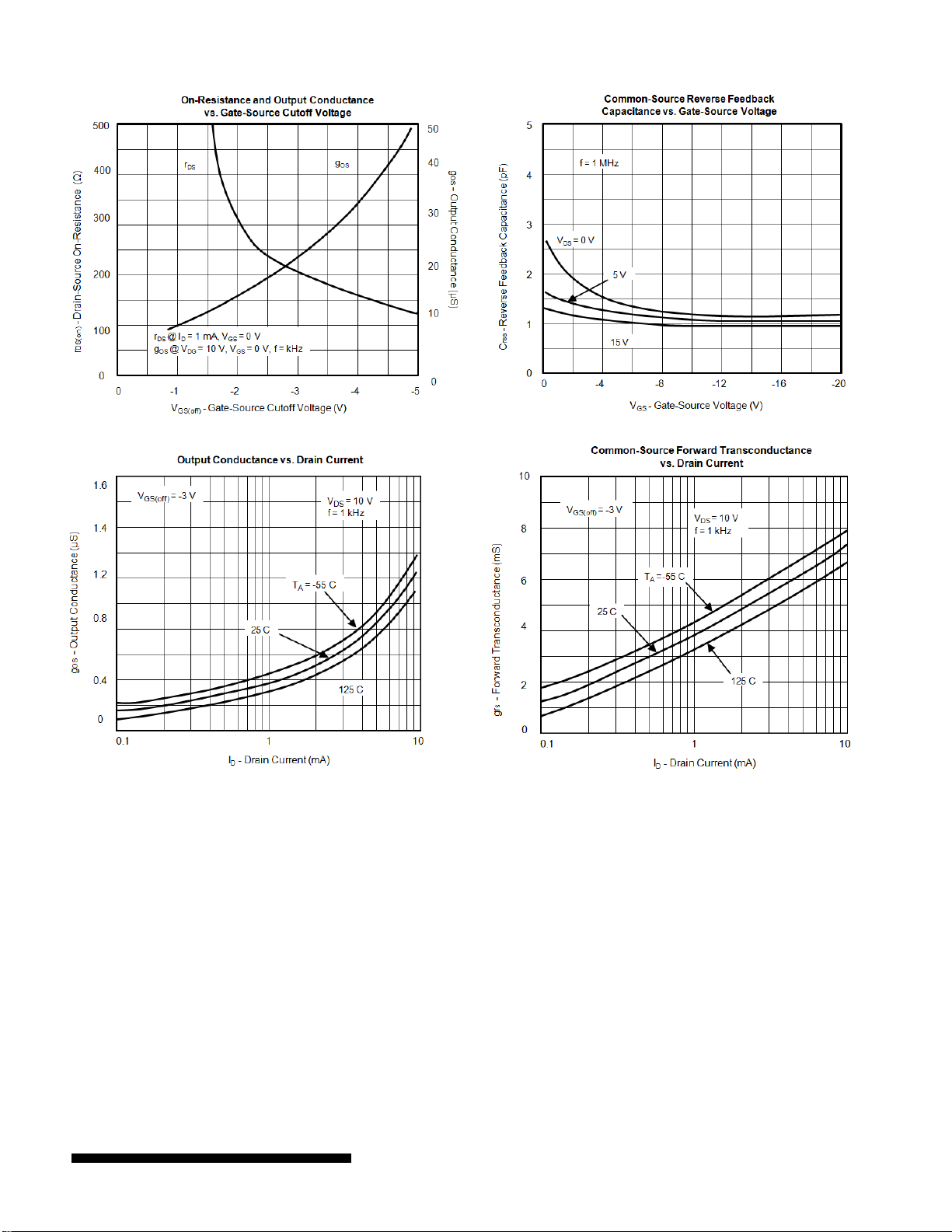
Typical Characteristics (Cont’d)
Page 6
Linear Integrated Systems
• 4042 Clipper Court • Fremont, CA 94538 • Tel: 510 490-9160 • Fax: 510 353-0261
Doc 201151 05/14/2014 Rev#A30 ECN# LSK489
Typical Characteristics (Cont’d)
Linear Integrated Systems (LIS) is a 25-year-old, third-generation precision semiconductor company providing high-quality
discrete components. Expertise brought to LIS is based on processes and products developed at Amelco, Union Carbide, Intersil
and Micro Power Systems by company President John H. Hall. Hall, a protégé of Silicon Valley legend Dr. Jean Hoerni, was the
director of IC Development at Union Carbide, Co-Founder and Vice President of R&D at Intersil, and Founder/President of Micro
Power Systems.
 Loading...