

Page 1
BRUSHLESS DC MOTOR CONTROLLER
GENERAL DESCRIPTION
The LS7560/LS7561 are CMOS integrated circuits designed to
control three or four phase brushless DC motors in a closed or
open loop configuration. The IC consists of a decoder which
provides proper commutation sequencing, a frequency-topulse width converter and error amplifier for closed loop motor
speed control, a PWM comparator and sawtooth oscillator for
external driver power control and a 5.5V reference generator
for supplying power to motor sensors. Also included is Fault
detection and indication, overcurrent sensing, dynamic motor
braking, forward/reverse input, sensor spacing selections and
an enable input control. The overcurrent sense condition will
disable all output drivers when using the LS7560 and only the
bottom drivers when using the LS7561.
The IC operates from 10V to 18V and provides CMOS compatible outputs for interfacing with external power devices.
Operating below 10V will activate a Fault Indication Output
and disable all Output Drivers.
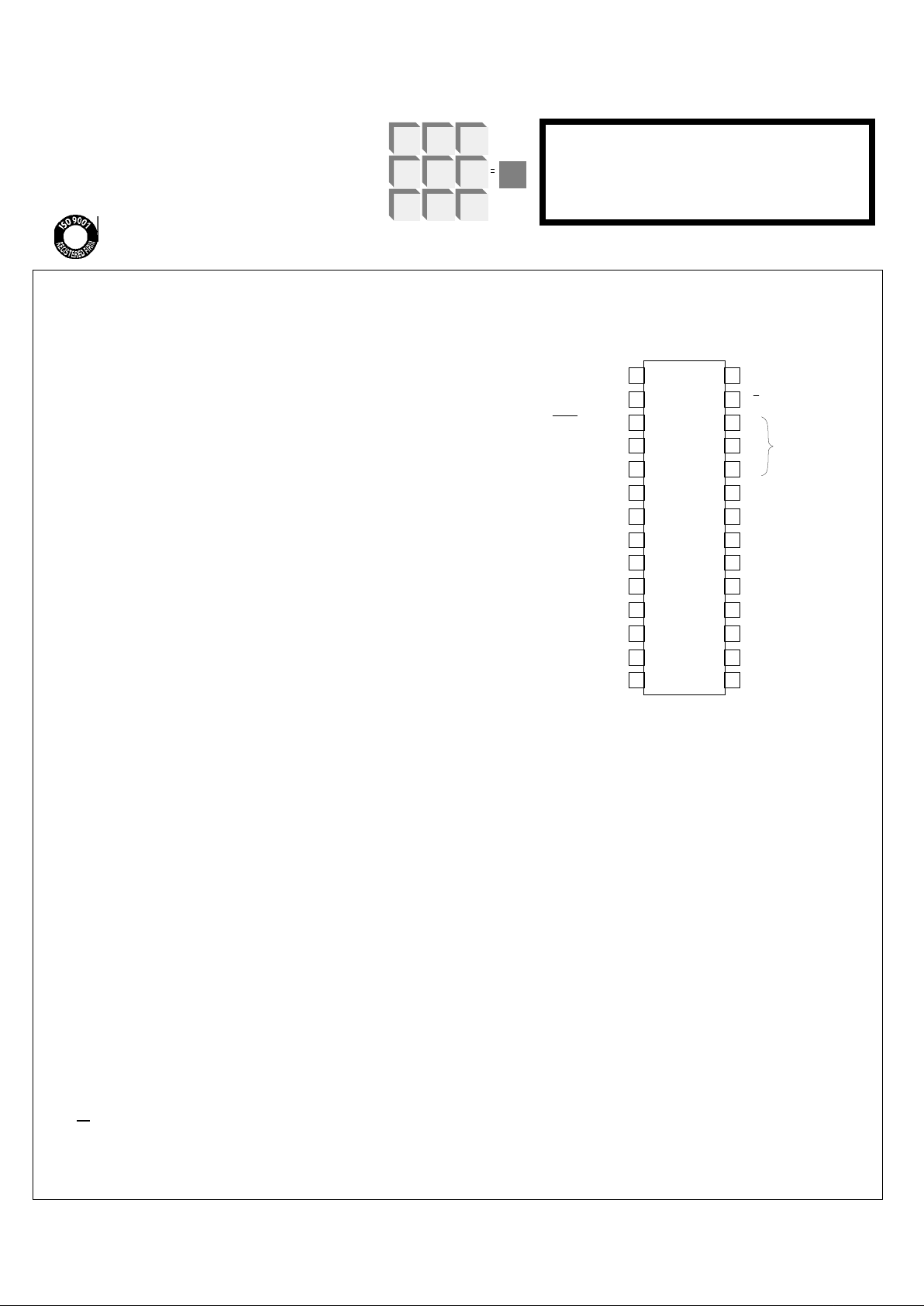
INPUT/OUTPUT DESCRIPTION: (See Figure 2)
SEQUENCE SELECT Input (Pin 1 )
A High on this input selects 60°/300° and a Low selects 120°/
240° electrical sensor separation. Use of a 300° or 240° motor
will cause opposite direction rotation as compared to a 60° or
120° motor.
F/R Input (Pin 27)
A High on this input selects Forward direction and a Low selects Reverse direction. The motor drive outputs are disabled
for 2 clock cycles at the onset of a direction change.
July 2002
7560-030599-1
1
2
3
4
5
6
7
8
9
10
11
12
13
14 15
16
17
18
19
20
21
22
23
24
25
26
27
28
FIGURE 1. PIN CONNECTION DIAGRAM
LS7560
SEQUENCE SELECT
ENABLE
FAULT INDICATOR
RC
TACHOMETER OUT
ERROR AMP (+)
ERROR AMP (-)
OSCILLATOR
ERROR AMP OUT
CURRENT SENSE (+)
CURRENT SENSE (-)
OUT 6
OUT 5
OUT 4
OUT 3
OUT 2
OUT 1
VSS (-V)
VR
TOP DRIVER POLARITY SELECT
PWM CONTROL
BRAKE SELECT
BRAKE
S1
S2
S3
F/R
VDD (+V)
HALL
SENSORS
TOP VIEW
S1, S2, S3 Inputs (Pins 24, 25, 26)
Hall Sensor inputs which are decoded to determine the Motor
Commutation Sequence. An invalid input code disables all motor
outputs. Inputs have Schmitt Trigger buffers for noise immunity.
BRAKE Input (Pin 23)
With the BRAKE SELECT input Low, a High on the BRAKE input
forces the Top Drivers to an OFF condition and the Bottom Drivers
to a PWM ON condition. If the Motor is under Closed Loop control,
the Loop is automatically opened and the error amplifier output is
connected to the Error Amp (-) input. By controlling the voltage at
teh Error Amp (+) input, the PWM duty cycle is controlled during
braking. This manner of braking prevents the Bottom Motor Drivers
from drawing excessive current, a condition which can occur during
normal braking, when the Bottom Drivers are turned ON unconditionally. With the BRAKE SELECT input High, a High on the
BRAKE input unconditionally causes the Top Drivers to turn OFF
and the Bottom Drivers to turn ON. The BRAKE function has priority over all other functions.
BRAKE SELECT Input (Pin 22)
A Low on this input selects PWM control of braking and a High selects unconditional braking.
ENABLE Input (Pin 2)
When the ENABLE input is above VR/2, all Output Drivers are enabled and when it is below VR/2.2, all Output Drivers are disabled.
This input has a nominal hysteresis of .05VR, where VR is the internally generated Reference Voltage available on Pin 19. Because
the ENABLE input is level sensitive, it can easily be used to control
operation of the IC based on an Analog Fault Condition.
LSI/CSI
LSI Computer Systems, Inc. 1235 Walt Whitman Road, Melville, NY 11747 (631) 271-0400 FAX (631) 271-0405
U
L
®
A3800
FEATURES
• Open loop motor control
• Tachometer output for closed loop motor control
• Error Amplifier and PWM Speed Comparator with full accessibility
• High noise immunity Schmitt Triggers on Sensor inputs
• 5.5V Reference Supply for external sensors
• Cycle-by-cycle current sensing
• Static, or current limited dynamic, motor braking
• Output enable delay on speed direction reversal
• Enable input with fault sensing capability
• Fault Indicator output
• 60°/300° or 120°/240° electrical sensor spacing selection
• Selectable PWM of top and bottom drivers or bottom drivers only
• CMOS compatible motor outputs with drive capability
• Selectable top driver polarity
• Low power dissipation
• +10V to +18V operation (VDD-Vss)
• LS7560, LS7561 (DIP); LS7560-SD, LS7561-SD (Skinny DIP);
LS7560-S, LS7561-S (SOIC); LS7560-TS, LS7561-TS (TSSOP)
See Figure 1
LS7560
LS7561
Page 2

ERROR AMPLIFIER Inputs (Pins 6, 7 ) Output (Pin 8)
For closed loop control, the TACHOMETER Output is applied
through a resistor to the negative input of the Error Amplifier on
Pin 7. A speed control potentiometer is connected to the positive
input of the Error Amplifier on Pin 6. A parallel RC Network is connected between the Output of the Error Amplifier on Pin 8 and Pin
7. The Amplifier, configured this way, enables the variable pulse
width to be converted to a DC voltage which is used to control the
motor speed. The potentiometer is used to set the desired motor
speed. For open loop control, configure the Error Amplifier as a
voltage follower by connecting Pin 7 directly to Pin 8 and do not
connect the TACHOMETER Output signal to the Error Amplifier.
TOP DRIVER POLARITY SELECT Input (Pin 20)
A High on this input selects a High Polarity for the Top Output
Drivers Motor ON condition and a Low selects a Low Polarity.
OUTPUT DRIVERS (Pins 12, 13, 14, 15, 16, 17)
Each Driver Output provides a CMOS compatible signal for driving Buffers/Power Transistors. The Outputs are capable of sinking/sourcing 25mA with a 1.5V drop across the IC, at VDD = 12V.
FAULT INDICATOR Output (Pin 3)
Open drain output to provide sinking current for driving an external device such as an LED to indicate a malfunction condition.
The output occurs under any of the following conditions:
1) Overcurrent Sense condition
2) ENABLE Input below VR/2.2
3) Invalid Sensor code
4) Chip power supply less than 9V
5) VR Output less than 4.1V
VR Output (Pin 19)
5.5V Reference Voltage Output that can supply 20mA of current
at VDD =12V for powering input Sensors.
VDD (Pin 28)
VDD is Supply Voltage positive terminal.
OSCILLATOR (Pin 9)
An external RC network is connected to this input to set the frequency of the Sawtooth Schmitt Trigger Oscillator. The Sawtooth
is applied to the PWM Comparator along with the output of the Error Amplifier. The output of the PWM Comparator is a Pulse
Width Modulated Signal which is used to vary the effective drive
to the motor and, hence, the motor speed.
OVERCURRENT SENSE (Pins 10, 11)
The input to Pin 10 comes from the high side of a fractional ohm
current sensing resistor. The voltage at this input is compared to
an internal 100mV Reference. When the voltage exceeds the
100mV Reference, an Overcurrent Condition exists and the Output Drivers are switched OFF until the end of the sawtooth oscillator ramp-up. When the sawtooth switches low, the Overcurrent Condition is sampled, and if it no longer exists, the Output
Drivers are switched ON again. Otherwise, the Output Drivers remain OFF until the end of the next sawtooth. The input to Pin 11
comes from the low side (Gnd) of the current sensing resistor and
connects to the low side of the internal 100mV Reference.
PWM CONTROL Input (Pin 21)
A High on this input causes only the Bottom Drivers to be Pulse
Width Modulated. A Low on this input causes both Top and Bottom Drivers to have PWM.
TACHOMETER Output (Pin 5)
The output of the Frequency To Pulse Width Converter is tied to
this pin. The Converter uses the three SENSOR Inputs and external RC Network to generate a variable frequency output with a
fixed positive pulse width.
RC Input (Pin 4)
The external RC network connected to this input programs the
positive pulse width of the Frequency to Pulse Width Converter.
VSS (Pin 18)
VSS is Supply Voltage negative terminal.
7560-040198-2
MAXIMUM RATINGS (Voltages referenced to Vss)
SYMBOL VALUE UNIT
Power Supply Voltage VDD 20 V
Voltage at any input VIN Vss - 0.3 to VR V
Operating Temperature TA -25 to +85 °C
Storage Temperature TSTG -65 to +150 °C
Output Drive Sink/Source Current Io 75 mA
VR Output Source Current IR 30 mA
ELECTRICAL CHARACTERISTICS
VDD = 12V, RT = 47kΩ, CT = 0.001µF, RS = 10kΩ, CS= 0.01µF (See Figure 3) TA = 25°C, unless otherwise specified
PARAMETER SYMBOL MIN TYP MAX UNIT
Reference Voltage VR 4.75 5.5 6.25 V
Line Regulation ∆VR - 100 200 mV
VDD = 10V to 18V, IREF =1.0mA
Temperature Stability
TA = 0°C to 70°C ∆VR - +/- 1.0 - %
TA = 0°C to 85°C ∆VR - +/- 1.3 - %
Error Amplifier:
Input Offset Voltage VIO - 5 15 mV
Input Current IIN - 0 10 nA
Input Common Mode Voltage Range VICR (0 to VR) V
Open Loop Voltage Gain (RL=15KΩ) AVOL 70 80 - dB
Common Mode Rejection Ratio CMRR 60 - - dB
Power Supply Rejection Ratio PSRR 60 - - dB
Page 3

PARAMETER SYMBOL MIN TYP MAX UNIT
Output High State (RL=15kΩ to Ground) VOH VR - - V
Output Low State (RL = 15kΩ to VR) VOL - - 1.0 V
Output Source or Sink Current Io - - 1.0 mA
Oscillator:
Oscillator Frequency FOSC 21 24 27 kHz
Percentage Frequency Change per Volt ∆F OSC ∆V - 0.4 1.0 %/V
(VDD = 10V to 18V) F
Sawtooth High Voltage VOSCP - 3.8 4.5 V
Sawtooth Low Voltage VOSCV 0.7 1.0 - V
Capacitor Discharge Current ID 0.6 1.0 2.5 mA
Logic Inputs:
Input Threshold Voltage VIH 3.0 2.3 - V
(Pins 1, 20, 21, 22, 23, 24, 25, 26, 27) VIL - 1.8 1.4 V
Brake and Sensor (Pins 23, 24, 25, 26)
High State Input Current (VIN = 4V) IIH -36 -27 -20 µA
Low State Input Current (VIL = 0V) IIL -50 -40 -30 µA
Sequence Select, Top Driver Polarity
Select, PWM Control, Brake Select,
and F/R Select (Pins 1, 20, 21, 22, 27)
High State Input Current (VIN = 4V) IIH -16 -12 -8 µA
Low State Input Current (VIL = 0V) IIL -25 -17 -10 µA
ENABLE Input Threshold Voltage (Pin 2) VIH 2.1 2.8 3.2 V
Hysteresis VH 0.2 0.3 0.4 V
ENABLE Input Current IIN - - 10 nA
Overcurrent Sense Comparator:
Input Threshold Voltage VIH 85 100 115 mV
Input Current IIN - - 10 nA
Outputs:
Closed Loop Control Section:
Tachometer Out
Output High Voltage (Isource = 1.5mA) VOH VR - 0.8 VR - 0.5 VR-.3 V
Output Low Voltage (ISINK = 5mA) VOL 0.18 0.27 0.40 V
Pulse Width TW 95 105 115 µs
Capacitor Discharge Current (RC Terminal) ID 1.8 3 7.5 mA
Output Drivers (Pins 12, 13, 14, 15, 16, 17)
Sourcing 25mA VOH 9.5 10.5 11 V
Sourcing 50mA VOH 8 8.8 9.5 V
Sinking 25mA VOL 1.0 1.30 2.0 V
Sinking 50mA VOL 2.75 3.40 4.2 V
Switching Times TR 30 45 60 ns
(CL = 250pF) TF 35 50 65 ns
Switching Times TR 100 150 200 ns
(CL = 1000pF) TF 130 180 230 ns
FAULT Output Voltage (ISINK = 16mA) VFO 47 - - kΩ
FAULT Off-State Leakage IF - 10 - nA
Under Voltage Lockout:
For VDD VUV 7.0 8.5 10 V
Hysteresis VH 0.45 0.65 0.85 V
For VR VUVR 3.5 4.1 4.8 V
Hysteresis VH 0.16 0.3 0.4 V
Power Supply Current
VDD = 10V IDD - 2.0 2.5 mA
VDD = 12V IDD - 3.0 4.0 mA
VDD = 18V IDD - 7.0 11.0 mA
7560-040298-3
Page 4

S
Q
S
R
Q
OSC.
SENSOR
Inputs
F/R
ENABLE
In
RC In
TACHOMETER
Out
VR
_
ERROR
AMP
_
PWM
GEN.
VR/2
FREQUENCY
TO
PULSE WIDTH
CONVERTER
DECODER
SEQUENCE
SELECT In
REFERENCE
GENERATOR
EDGE TRIGGERED
DELAY
FAULT INDICATOR Out
PWM CONTROL
In
BRAKE In
O1
O2
O3
O6
O5
O4
TOP DRIVER
POLARITY SELECT In
TOP
DRIVER
Outputs
BOTTOM
DRIVER
Outputs
+
_
+
+
+
_
BRAKE SELECT
FIGURE 2. LS7560/LS7561 MOTOR CONTROLLER BLOCK DIAGRAM
OVERCURRENT
SENSE In
17
16
15
14
13
12
22
23
8
6
7
5
4
2
27
VR
26
24
19
25
10
11
9
NC FOR LS7560
VDD FOR LS7561
20
21
3
1
7560/61-030599-4
R
VDD
VSS
28
18
INTERNAL BOND PAD
+
100mV
-
VR VR
VR
VR
VR
VR
VR
LOW VDD
DETECT
VDD
SWITCH
VDD
SWITCH
VDD
VR
CONTROL
CONTROL
VDD
VDD
VDD
VDD
VDD
VDD
LOW VR DETECT
ERROR AMP (-)
ERROR AMP (+)
ERROR AMP Out
OSCILLATOR
+V
-V
SWITCH
Page 5

7560-120497-5
7
8
6
19
9
VR
OSC
ERROR AMP(-)
ERROR AMP
OUT
ERROR AMP(+)
RT
CT
FIGURE 5. OPEN LOOP CONTROLLER
FIGURE 5. In this configuration, the PWM output
duty cycle to the motor drivers is directly proportional to the DC voltage applied to Pin 6, since
Pins 7 and 8 are tied together.
OUT6
OUT5
OUT4
12
13
14
10
11
VM
ENABLE
BRAKE
23
2
R
C
VR
FIGURE 4. THREE PHASE HALF WAVE MOTOR CONTROLLER
19
(+)
(-)
OVERCURRENT
SENSE
VR
24
25
26
27
21
20
22
15
16
17
14
13
12
10
11
5
7
8
6
9
4
3
28
18
19
2
1
23
ROTOR
OUT1
OUT2
OUT3
OUT4
OUT5
OUT6
S1
S2
S3
F/R
PWM CNTRL
TOP DRV
POL SEL
BRAKE SEL
BRAKE
OVERCURRENT
SENSE
SEQ SEL
TACH OUT
ENABLE
ERROR
AMP
OSC
RC
VR
VSS
VDD
FAULT
VM
VM
FIGURE 3. THREE PHASE CLOSED LOOP FULL WAVE MOTOR CONTROLLER
CS
VR
CT
RT
10K
R2
100K
C1
0.1µF
*
*
*
R1
TYPICAL
VALUES
*
1.0M
*
VR
S1
S2
S3
(-)
OUT
(+)
S1
S2
S3
Rs
(+)
(-)
R3
**
FIGURE 3. The closed loop mo-
tor control operation is achieved
by applying the Tachometer
Output at Pin 5 into the negative
terminal of the Error Amplifier
(Pin 7) through an R1-C1-R2 integrating network. The R1-C1
network is configured as a feedback circuit around the amplifier.
Since the Tachometer Output
has a fixed positive pulse width,
the average value of the pulse
train is directly proportional to
the motor speed. The desired
speed is selected by applying a
voltage at the positive input
(Pin 6) of the Error Amplifier.
The resultant output voltage of
the Error Amplifier is applied to
an internal Comparator along
with a ramp waveform generated by the RC Network at Pin
9. The PWM signal at the Comparator output is used to drive
outputs 1 thru 6 and complete
the closed loop. For this configuration, Pin 20, the Top Driver
Polarity Select must be tied to
Ground.
FIGURE 4. This three phase half wave motor controller has no top power transistor to disconnect the windings from the power supply when the BRAKE is applied. Instead, a switching transistor is used which will permit braking for a time
determined by the RC time constant. When the capacitor discharges past the
ENABLE input switching point, the outputs will be turned off.
Page 6

7560-082197-6
17
15
14
12
10
11
ROTOR
3
1
2
4
24
25
26
S1
S2
S3
20
VM
OUT1
OUT3
OUT4
OUT6
FIGURE 6. FOUR PHASE FULL WAVE MOTOR CONTROLLER
23
BRAKE
TOP
DRIVER
POLARITY
SELECT
VM
S1
S2,S3
OVERCURRENT
SENSE
(+)
(+)
VM
S1
S2,S3
FIGURE 6. Four phase motor control requires only two Hall Sensor inputs spaced 90 electrical
degrees apart. S1 is connected to one sensor and S2 and S3 are tied together and connected to
the other sensor (Refer to Table 1). The BRAKE input (Pin 23) is used to control the Top Driver
Select (Pin 20) and the Top Motor Drivers. When the BRAKE input is applied, the Top Motor drivers are turned off and the Top Driver Polarity Select is forced low turning on the Outputs 1 and 3.
Since Outputs 4 and 6 are also turned on, the motor windings become shorted together.
The information included herein is believed to be
accurate and reliable. However, LSI Computer Systems,
Inc. assumes no responsibilities for inaccuracies, nor for
any infringements of patent rights of others which may
result from its use.
Page 7

11
14
10
17
15
12
VM
OUT1
OUT3
OUT4
OUT6
VR
FIGURE 7. FOUR PHASE HALFWAVE MOTOR CONTROLLER
19
2
20
23
ENABLE
TOP DRIVER
POLARITY
SELECT
BRAKE
(+)
(-)
OVERCURRENT
SENSE
22
23
5
7
6
8
BRAKE
SELECT
BRAKE
TACH OUT
OUT
VR
VR
(-)
(+)
ERROR
AMP
1M
100K
SPEED
CONTROL
PWM RATE
CONTROL
FIGURE 8. PWM BRAKING
0.1µF
VR
BRAKE
BRAKE
BRAKEBRAKE
BRAKEBRAKE
BRAKE
BRAKE
BRAKE
BRAKE
TYPICAL
VALUES
*
*
*
*
R2
R1
C1
FIGURE 7. This four phase half wave motor controller uses the same BRAKE circuit as in Figure 4 and switches
the Top Driver Select from a high to a low as in Figure 6.
FIGURE 8. Using an analog switch (such as the CD4066) PWM braking can be employed when the brake is
applied. At that time, the error amplifier is configured as a voltage follower and its input is switched from the
speed adjustment control to the PWM rate control. By adjusting the PWM rate control, the average motor
current during braking can be controlled.
7560-040198-7
Page 8

TABLE 1. OUTPUT COMMUTATION SEQUENCE FOR THREE PHASE OPERATION
LS7560
SENSOR ELECTRICAL
SEPARATION TOP BOTTOM
60° 120° DRIVERS DRIVERS
S1, S2, S3 S1, S2, S3 F/R EN BRK OCS O1, O2, O3 O4, O5, O6 FAULT
0 0 0 0 0 1 1 1 0 0 0 1 1 0 1 0 1
1 0 0 1 0 1 1 1 0 0 1 1 0 0 1 0 1
1 1 0 1 0 0 1 1 0 0 1 1 0 1 0 0 1
1 1 1 1 1 0 1 1 0 0 1 0 1 1 0 0 1
0 1 1 0 1 0 1 1 0 0 1 0 1 0 0 1 1
0 0 1 0 1 1 1 1 0 0 0 1 1 0 0 1 1
0 1 0 0 0 0 X X 0 X 1 1 1 0 0 0 0
1 0 1 1 1 1 X X 0 X 1 1 1 0 0 0 0
0 0 0 0 0 1 0 1 0 0 1 0 1 1 0 0 1
1 0 0 1 0 1 0 1 0 0 1 0 1 0 0 1 1
1 1 0 1 0 0 0 1 0 0 0 1 1 0 0 1 1
1 1 1 1 1 0 0 1 0 0 0 1 1 0 1 0 1
0 1 1 0 1 0 0 1 0 0 1 1 0 0 1 0 1
0 0 1 0 1 1 0 1 0 0 1 1 0 1 0 0 1
0 1 0 0 0 0 X X 0 X 1 1 1 0 0 0 0
1 0 1 1 1 1 X X 0 X 1 1 1 0 0 0 0
X X X X X X X X 1 X 1 1 1 1 1 1 1
X X X X X X X X 0 1 1 1 1 0 0 0 0
X X X X X X X 0 0 X 1 1 1 0 0 0 0
NOTE 1: This Table assumes the TOP DRIVER POLARITY SELECT (Pin 20) = Logic 0. For Pin 20 = Logic 1,
invert the polarity of the top drivers.
NOTE 2: For the LS7561, the OVERCURRENT SENSE = Logic 1 only forces the bottom drivers to a Logic 0.
It has no effect on the top driver outputs which are determined by the other inputs as shown in the table.
EN = ENABLE
BRK = BRAKE
OCS = OVER
CURRENT
SENSE
TABLE 2. OUTPUT COMMUTATION SEQUENCE FOR FOUR PHASE OPERATION
LS7560
SENSOR ELECTRICAL
SEPARATION = 90° TOP BOTTOM
DRIVERS DRIVERS
S1 S2, S3 F/R EN BRK OCS O1, O3 O4, O6 FAULT
0 0 1 1 0 0 1 0 0 0 1
1 0 1 1 0 0 0 1 0 0 1
1 1 1 1 0 0 0 0 1 0 1
0 1 1 1 0 0 0 0 0 1 1
0 0 0 1 0 0 0 0 1 0 1
1 0 0 1 0 0 0 0 0 1 1
1 1 0 1 0 0 1 0 0 0 1
0 1 0 1 0 0 0 1 0 0 1
X X X X 1 X 0 0 1 1 1
X X X X 0 1 0 0 0 0 0
X X X 0 0 X 0 0 0 0 0
NOTE 1: SEQUENCE Input (Pin 1) set at a Logic 1.
NOTE 2: This Table assumes theTOP DRIVER POLARITY SELECT (Pin 20) = Logic 1. For Pin 20 = Logic 0, invert the
polarity of the top drivers.
NOTE 3: For the LS7561, the OVERCURRENT SENSE = Logic 1 only forces the bottom drivers to a Logic 0. It has no
effect on the Top Driver Outputs which are determined by the other inputs as shown on the table.
EN = ENABLE
BRK = BRAKE
OCS = OVER
CURRENT
SENSE
7560-102597-8
 Loading...