

Page 1
DELAYED-OFF LIGHT SWITCH
WITH PROGRAMMABLE ON-TIMER
FEATURES:
• Phase-Lock Loop Synchronization allows use in
Wall Switch Applications.
• Operation automatically sequences from Timed-On to
Delayed-Off to Off.
• On-Timer programmable with external R-C.
• Transition from Timed-On to Delayed Off indicated by
31% drop in Delivered Power.
• Delayed-Off period denoted by Dim-to-Off operation.
(See Note 1)
• Control input initiates Operating Sequence and can override
Automatic Sequencing.
• 50/60Hz Line Frequency.
• +12V to +18V Operation (VSS - VDD).
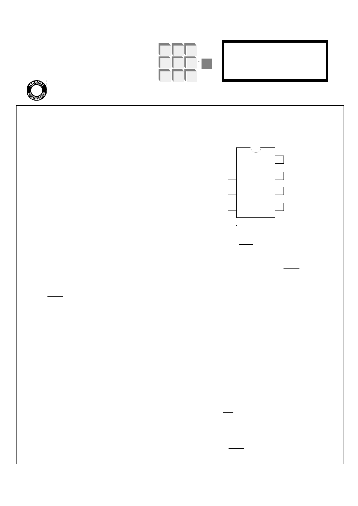
• LS7338 (DIP); LS7338-S (SOIC) - See Figure 1
NOTE 1: Dim-to-Off time is Mask Programmable. The standard
IC is fixed at 209 seconds for 60Hz. Dim-to-Off time can be programmed within a range of 6.5 to 836 seconds.
APPLICATIONS:
• WALL SWITCH for incandescent lighting in garage, corridor,
staircase, child’s bedroom, teenage study area.
• IN-LINE SWITCH for table lamps.
DESCRIPTION:
The LS7338 is a monolithic MOS integrated circuit designed to turn a
triac On and Off in a Power Switch for Incandescent Lighting. Activation of SENSE or SLAVE inputs turns the triac On and starts a
timer. The triac remains On for the duration of the Timer which is
controlled by an external R-C connected to the OSCILLATOR input.
When Time-out occurs, the power delivered by the triac is stepped
down by 31% and then slowly reduced to Off over a fixed period of
time.
In a typical application (Figure 5), the output of the LS7338 drives
the gate of a triac in series with the load.
There are three states through which the LS7338 can be stepped.
The states and their corresponding operating mode, phase angles
and delivered power levels are shown in Table 1.
OPERATING DESCRIPTION:
Upon power up, internal power-on-reset starts the LS7338 in
STATE 0. When the SENSE input transitions to logic 0, or the
SLAVE input transitions to logic 1, the IC steps to STATE 1.
When implemented as shown in the application example (Figure 5), this is accomplished by touching the appropriate Sensor
Plate. Subsequent similar transitions at SENSE or SLAVE inputs cause the LS7338 to step through the sequence:
STATE 0 --> STATE 1 --> STATE 2 --> STATE 0, etc.
STATE 1 and STATE 2 are quasi-stable states. If left in STATE
1, after a time-out period determined by the frequency set at
the OSC input (See I/O Description, Pin 6), the IC automatically
steps to STATE 2. (If the OSC input is deactivated, STATE 1
becomes stable and its OPERATING MODE is denoted as On).
When the IC steps from STATE 1 to STATE 2, the output
phase angle ø changes from 159˚ to 107˚. This corresponds to
a delivered power reduction of 31%, which causes a reduction
of lamp brightness. This brightness change provides the user
with a positive indication that the transition from STATE 1 to
STATE 2 has occurred. The Time-out period for STATE 2 is
fixed at 209 seconds for 60Hz operation. (See Note 1.)
TD1 = STATE 1 Time-out period.
TD2 = STATE 2 Time-out period.
June 2001
LSI/CSI
LSI Computer Systems, Inc. 1235 Walt Whitman Road, Melville, NY 11747 (631) 271-0400 FAX (631) 271-0405
LS7338
U
L
®
A3800
7338-062001-1
1
2
3
4
5
6
7
LSI
8
PIN ASSIGNMENT - TOP VIEW
FIGURE 1
SENSE
SLAVE
VDD(-V)
TRIG
VSS (+V)
SYNC
CAP
OSC
LS7338
TABLE 1
(See Figures 2 and 3) STATE 0 STATE 1 STATE 2
OPERATING MODE OFF Timed-On Delayed -Off
PHASE ANGLE, ø No Output 159˚ 107˚ to 41˚
% LOAD POWER (1) 0 99 68 to 7
During the STATE 2 Time-out, the TRIG phase angle ø (See
Figure 2) is ramped down from 107˚ to 41˚ in decrements of
1.4˚. When ø reaches 41˚, the IC automatically steps to STATE
0, shutting the TRIG and lamp Off.
The slow Dim-to-Off in STATE 2 gives the user a continuing reminder that Delayed-Off is operating and provides the time and
light with which to leave the area or to recycle the Light Switch.
A new operating sequence from STATE 0 can be started only by
transitions at the SENSE and SLAVE inputs.
(1) The percentage of full power delivered to a resistive load by the
triac switch.
Page 2
INPUT/OUTPUT DESCRIPTION:
SENSE (Pin 1)
A logic 0 applied to this input for a minimum of three SYNC cycles, TS1 (50ms for 60Hz, 60ms for 50Hz), causes the circuit to
step to the next state in the operating sequence.
SLAVE (Pin 2)
Same description as SENSE (Pin 1) except that logic 1 replaces
logic 0. This input is designed to be used with Remote Extensions (See Figure 5 and Figure 6.)
VDD (Pin 3)
Supply voltage negative terminal.
TRIG (Pin 4)
TRIG is a negative-going pulse occurring once every half cycle
of the SYNC input. Pulse width is 33µs. Table 1 in the General
Description shows values of the TRIG phase angle for the different states. (See Figure 2 and Figure 3.)
VSS (Pin 5)
Supply voltage positive terminal.
OSC (Pin 6)
An R-C network connected to this input controls the frequency of
oscillation which determines the Time-out, TD1, in State 1. TD1 is
approximately 255RC. The Oscillator is active only in State 1. Chip
to chip Oscillation Tolerance is ±10% for fixed value of RC. Tie Pin
6 to VSS if a Time-out is not desired. (See Figure 5.)
CAP (Pin 7)
The CAP input is for external component connection for the PLL filter capacitor. (See Figure 5.)
SYNC (Pin 8)
The AC Line Frequency (50/60Hz) is applied to this input. The
Phase-Lock Loop synchronizes all internal timings to the AC signal
at the SYNC input. (See Figure 5.)
7338-112497-2
ABSOLUTE MAXIMUM RATINGS:
PARAMETER SYMBOL VALUE UNIT
DC supply voltage VSS - VDD +20 V
Any input voltage VIN VSS-20 to VSS + .5 V
Operating temperature TA 0 to +85 °C
Storage temperature TSTG -65 to +150 °C
DC ELECTRICAL CHARACTERISTICS:
(TA = 25°C, all voltages referenced to VDD)
PARAMETER SYMBOL MIN TYP MAX UNIT CONDITIONS
Supply Voltage VSS +12 - +18 V Supply Current ISS - 1.6 2.2 mA VSS = +15V,
Output off
Input Voltages
SYNC Lo VIRL 0 - VSS-9.5 V -
SYNC Hi VIRH VSS-5.5 - VSS V SENSE Lo VIOL 0 - VSS-8 V SENSE Hi VIOH VSS-2 - VSS V SLAVE Lo VIVL 0 - VSS-8 V SLAVE Hi VIVH VSS-2 - VSS V -
Input Current
SYNC, SENSE & IIH - - 110 uA With Series 1.5MΩ
SLAVE Hi Resistor to 115VAC
SYNC, SENSE &
SLAVE Lo IIL - - 100 nA -
TRIG Hi Voltage VOH - VSS - V TRIG Lo Voltage VOL - VSS-8 - V VSS = +15V
TRIG Sink Current IOS 25 - - mA VSS = +15V,VOL = VSS -4V
TRANSIENT CHARACTERISTICS (See Fig. 2 and 3)
(All timings are based on Fs = 60Hz, unless otherwise specified.)
PARAMETER SYMBOL MIN TYP MAX UNIT
SYNC Frequency Fs 40 - 70 Hz
SENSE/SLAVE Sense Time Ts1 50 - Infinite ms
TRIG Pulse Width Tw - 33 - µs
STATE 1 Time-out period TD1 - 255RC - s
STATE 2 Time-out period TD2 - 209 - s
Page 3

7338-112497-3
Tw Tw
ø
FIGURE 2. OUTPUT CONDUCTION ANGLE, Ø
SYNC
TRIG
SENSE
SLAVE
Ø
TS1
<TD1 TS1
TS1
TS1
TD2
TD1<TD2
OFF/STATE 0
OFF/ STATE 0
159˚/STATE 1
107˚/STATE 2
< 41˚/STATE 2
159˚/STATE 1
FIGURE 3. OUTPUT PHASE ANGLE ø VS
SENSE AND SLAVE
OFF/STATE 0
107˚/STATE 2
41˚/STATE 2
DIGITAL
COMPARATOR
ø DECODE
SYNC
PHASE-ANGLE
POINTER
PHASELOCK
LOOP
CONTROL
LOGIC
BUF
BUF
BUF
SYNC
CAP
SENSE
SLAVE
VSS
VDD
FIGURE 4. LS7338 BLOCK DIAGRAM
TRIG
OSC/TIMER
OSC
(+V)
(-V)
DRIVER
4
8
7
1
2
6
5
3
The information included herein is believed to be
accurate and reliable. However, LSI Computer Systems,
Inc. assumes no responsibilities for inaccuracies, nor for
any infringements of patent rights of others which may
result from its use.
Page 4

P
AC
MAINS
N
LOAD
C1
T1
L1
C2
R1
R2
A
B
R6
R9
C3
D1
5 6 7 8
4 3 2
1
R5
C3
C4
OUT
VDD SLV SENSE
VSS OSC CAP SYNC
+
LS7338
R4
R3
SEE NOTE 1
FIGURE 5. A TYPICAL LIGHT SWITCH APPLICATION
G
MT2
MT1
Z1
-
ELECTRONIC
EXTENSION
(Figure 6)
EXTN
P
C7
SEE NOTE
3
SEE NOTE 2
R10
SENSOR
PLATE
R8
C6
R7
- +
NOTES: 1. Use Connection A when Neutral is not available. Use Connection B when Neutral is available.
2. C7 is used only with Electronic Extension. R10 is used only with Mechanical Switch.
3. Connection between Pin 2 and Pin 3 is removed when SLAVE input is used.
4. See Table 2 for Component Functional Description
115VAC 220VAC 115VAC 220VAC
(1)R1 270Ω, 1W 1kΩ, 2W (1) C2 0.33µF,200V 0.22µF,400V
(2)R1 82Ω 82Ω (2) C2 0.22µF,200V 0.1µF,400V
R2 1.5MΩ 1.5MΩ C3 47µF 47µF
R3 2.7MΩ 4.7MΩ C4 470pF 470pF
R4 2.7MΩ 4.7MΩ C5 .047µF .047µF
(3)R5 1MΩ to 5MΩ 1MΩ to 5MΩ C6 (5) (5)
R6 100Ω 100Ω C7 0.1µF,200V 0.1µF,400V
R7 (4) (4) Z1 15V, 1/2W 15V, 1/2W
R8 (4) (4) D1 1N4148 1N4148
R9 1.5MΩ 1.5MΩ L1 100µH 200µH
R10 150kΩ 150kΩ (6) T1 Q4008L4 Q5004L4
C1 0.15µF, 200V 0.15µF, 400V
(1) Connection A
(2) Connection B
(3) Select for desired touch sensitivity
(4) 100kΩ ≤ (R7 + R8) ≤ 10MΩ
(5) (R7 + R8)C6 ≥ 5ms
(6) Typical
All Resistors 1/4W, all Capacitors 25V unless otherwise specified
TABLE 2 . FIGURE 5 COMPONENT FUNCTIONAL DESCRIPTION
COMPONENTS FUNCTIONAL DESCRIPTION
Z1, D1, R1, C2, C3 DC Power Supply.
R2, C4 Current limit and filter AC for SYNC input.
C1, L1 RFI filtering for AC Mains.
C5 PLL filter capacitor.
R3, R4, R5 Network sets the Touch Sensitivity
for the SENSE input.
R6 Current limiting and isolation between
IC output and Triac Gate.
R7, R8, C6 Oscillator R-C network.
Potentiometer R6 required only if providing
user adjustment of Time-out, TD1.
R9, C7 Filter for the Electronic Extension
R10 Current limiting resistor for
the Mechanical Switch Extension.
Page 5

EXTN
2KΩ,1/4W
IN914
SENSOR PLATE
2MΩ,1/4W
200KΩ,1/4W
P
MPS8599
FIGURE 6. ELECTRONIC SWITCH EXTENSION
2MΩ,1/4W
EXTENSIONS: (See Figure 5 and Figure 6)
All sequence functions can also be inplemented by utilizing the SLAVE input. This
can be done by either a mechanical switch or the electronic switch in conjunction with
a sensing plate as shown in Figure 6. When the plate is touched, a logic high level is
generated at the EXTENSION terminal for both half cycles of the line frequency.
 Loading...