

Page 1
24-BIT DUAL-AXIS QUADRATURE COUNTER
LS7266R1 Registers:
LS7266R1 has a set of registers associated with each X and Y axis. All X-axis registers have the name prefix X,
whereas all Y-axis registers have the prefix Y. Selection of a specific register for Read/Write is made from the decode
of the three most significant bits (D7-D5) of the data-bus. CS input enables the IC for Read/Write. C/D input selects
between control and data information for Read/Write. Following is a complete list of LS7266R1 registers.
December 2002
7266R1-121002-1
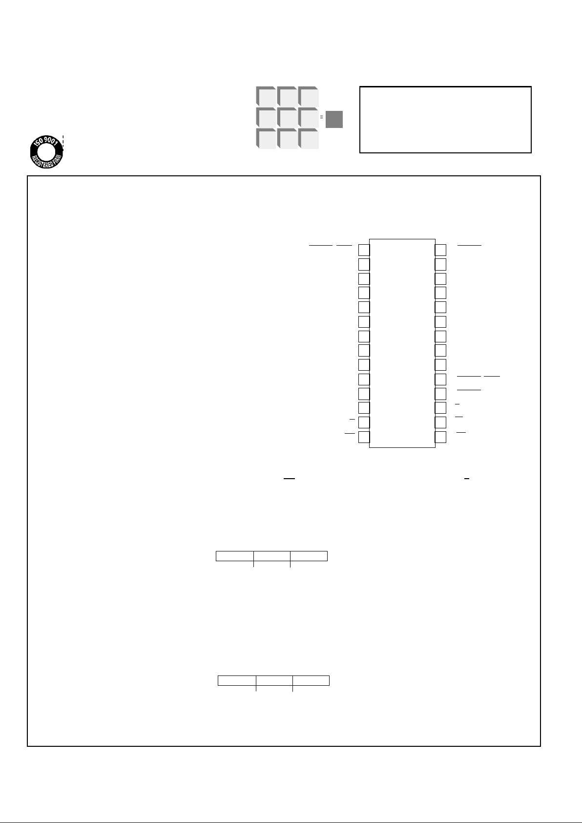
28
27
26
25
24
23
22
21
20
19
18
17
16
15
14
13
12
11
10
9
8
7
6
5
4
3
2
1
YLCNTR/YLOL
FCK
VDD (+5V)
D0
D1
D2
D3
D4
D5
D6
D7
VSS (GND)
C/D
WR
LS7266R1
CS
RD
XRCNTR/XABG
XLCNTR/XLOL
XA
XB
XFLG1
YA
YB
YFLG2
YFLG1
YRCNTR/YABG
XFLG2
X/Y
PIN ASSIGNMENT - TOP VIEW
28-Pin Package
Preset Registers: XPR and YPR
Each of these PRs are 24-bit wide. 24-bit data can be written into a PR, one byte at a time, in a sequence of three data
write cycles.
7 70 0 7 0
HI BYTE MID BYTE LO BYTE
PR
(PR2) (PR1) (PR0)
Output Latches: XOL and YOL
Each OL is 24-bits wide. In effect, the OLs are the output ports for the CNTRs. Data from each CNTR can be loaded
into its associated OL and then read back on the data-bus, one byte at a time, in a sequence of three data Read
cycles.
7 70 0
7
0
HI BYTE MID BYTE LO BYTE
OL
(OL2) (OL1) (OL0)
Counters: XCNTR and YCNTR
Each of these CNTRs are 24-bit synchronous Up/Down counters. The count clocks for each CNTR is derived from its
associated A/B inputs. Each CNTR can be loaded with the content of its associated PR.
Byte Pointers: XBP and YBP
The Read and Write operations on an OL or a PR always accesses one byte at a time. The byte that is accessed is
addressed by one of the BPs. At the end of every data Read or Write cycle on an OL or a PR, the associated BP is
automatically incremented to address the next byte.
FEATURES:
• 30 MHz count frequency in non-quadrature mode,
17MHz in x4 quadrature mode.
• Dual 24-bit counters to support X and Y axes in
motion control applications.
• Dual 24-bit comparators.
• Digital filtering of the input quadrature clocks
• Programmable 8-bit separate filter clock prescalers
for each axis.
• Error flags for noise exceeding filter band width.
• Programmable Index Input and other programmable I/Os.
• Independent mode programmability for each axis.
• Programmable count modes:
Quadrature (x1, x2, x4) / Non-quadrature,
Normal / Modulo-N / Range Limit / Non-Recycle,
Binary / BCD.
• 8-bit 3-State data I/O bus.
• 5V operation (VDD-VSS).
• TTL/CMOS compatible I/Os.
• LS7266R1 (DIP); LS7266R1-SD (Skinny DIP);
LS7266R1-S (SOIC); LS7266R1-TS (TSSOP)
LSI/CSI
LS7266R1
LSI Computer Systems, Inc. 1235 Walt Whitman Road, Melville, NY 11747 (631) 271-0400 FAX (631) 271-0405
U
L
®
A3800
Page 2
7 6 5 4 3 2 1 0
BT: Borrow Toggle flip-flop.
Toggles every time CNTR underflows.
CT: Carry toggle flip-flop.
Toggles every time CNTR overflows.
CPT: Compare toggle flip-flop.
Toggles every time PR equals CNTR.
S: Sign flag. Set to1 when CNTR underflows.
Reset to 0 when CNTR overflows.
FLAG
E: Error flag. Set to 1 when excessive noise is present at the count
inputs in quadrature mode. Irrelevant in non-quadrature mode.
U/D: Up/Down flag. Set to 1 when counting up
and reset to 0 when counting down.
Not used. Always reset to 0.
IDX: Index. Set to 1 when selected index input is at active level.
0
Filter Clock Prescalers: XPSC and YPSC
Each PSC is an 8-bit programmable modulo-N down counter, driven by the FCK clock. The factor N is down loaded
into a PSC from the associated PR low byte register PR0. The PSCs provide the ability to generate independent filter
clock frequencies for each channel. The PSCs generate the internal filter clock, FCKn used to
validate inputs XA, XB, YA, YB in the quadrature mode.
Final filter clock frequency fFCKn = ( fFCK/(n+1) ) , where n = PSC = 0 to FFH. For proper counting in the quadrature
mode, fFCKn ≥ 8fQA (or 8fQB), where fQA and fQB are the clock frequencies at inputs A and B. In non-quadrature mode
filter clock is not needed and the FCK input (Pin 2), should be tied to VDD.
7266R1-111196-2
Flag Register: XFLAG and YFLAG
The FLAG registers hold the status information of the CNTRs and can be read out on the data bus. The E bit of a
FLAG register is set to 1 when the noise pulses at the quadrature inputs are wide enough to be validated by the
input filter circuits. E = 1 indicates excessive noise at the inputs but not a definite count error. Once set, E can
only be reset via the RLD.
7 6 5 4 3 2 1 0
0: NOP
0
1
0
RLD
1: Reset BP
0
0
1
0
1
1
0
0 : Select the RLD addressed by X/Y input
1 : Select both XRLD and YRLD together
(Note: D7 = 1 overrides X/Y input)
: Select RLD
: NOP
: Reset CNTR
: Reset BT, CT, CPT,S
: Reset E
0
0
1
0
0
1
1
1
: NOP
: Transfer PR to CNTR
(Note: All 24-bits are transferred in parallel)
: Transfer CNTR to OL
(Note: All 24-bits are transferred in parallel)
: Transfer PR0 to PSC
Reset and Load Signal Decoders: XRLD and YRLD
Following functions can be performed by writing a control byte into an RLD: Transfer PR to CNTR, Transfer
CNTR to OL, reset CNTR, reset FLAG and reset BP.
:
Page 3
7266R1-111196-3
Counter Mode Registers: XCMR and YCMR
The CNTR operational mode is programmed by writing into the CMRs.
7 6 5 4 3 2 1 0
0 : Binary count
: Normal count
: Range Limit
: Non-recycle count
: Modulo-N
CMR
1 : BCD count
0
0
1
1
: Quadrature X1
0
: Non-quadrature
: Quadrature X2
1
: Quadrature X4
1
0: Select CMR addressed by X/Y input
1: Select both XCMR and YCMR together (Note: D7=1 overrides X/Y input)
: Select CMR
0
0
1
0
1
1
0
1
1
0
0
DEFINITIONS OF COUNT MODES:
Range Limit. In range limit count mode, an upper and a lower limit is set, mimicking limit switches in the me-
chanical counterpart. The upper limit is set by the content of the PR and the lower limit is set to be 0. The
CNTR freezes at CNTR = PR when counting up and at CNTR=0 when counting down. At either of these limits,
the counting is resumed only when the count direction is reversed.
Non-Recycle. In non-recycle count mode, the CNTR is disabled, whenever a count overflow or underflow takes
place. The end of cycle is marked by the generation of a Carry (in Up Count) or a Borrow (in Down Count). The
CNTR is re-enabled when a reset or load operation is performed on the CNTR.
Modulo-N. In modulo-N count mode, a count boundary is set between 0 and the content of PR. When counting
up, at CNTR=PR, the CNTR is reset to 0 and the up count is continued from that point. When counting down, at
CNTR=0, the CNTR is loaded with the content of PR and down count is continued from that point.
The modulo-N is true bidirectional in that the divide-by-N output frequency is generated in both up and down direction of counting for same N and does not require the complement of N in the UP instance. In frequency divider application, the modulo-N output frequency can be obtained at either the Compare (FLG1) or the Borrow
(FLG2) output. Modulo-N output frequency, fN = (fi / (N+ 1) ) where fi = Input count frequency and N = PR.
The information included herein is believed to be
accurate and reliable. However, LSI Computer Systems,
Inc. assumes no responsibilities for inaccuracies, nor for
any infringements of patent rights of others which may
result from its use.
Page 4
Input/Output Control Register: XIOR and YIOR
The functional modes of the programmable input and output pins are written into the IORs.
7 6 5 4 3 2 1 0
0 : Disable inputs A and B
0 : LCNTR/LOL pin is Load CNTR input
0 : RCNTR/ABG pin is Reset CNTR input
0
IOR
1 : Enable inputs A and B
1 : LCNTR/LOL pin is Load OL input
1 : RCNTR/ABG pin is A and B Enable gate
0
0
: FLG1 pin is COMPARE output; FLG2 pin is BORROW output
1
: FLG1 pin is CARRY output; FLG2 pin is BORROW output
: FLG1 pin is Carry/Borrow output and FLG2 pin is U/D (FLAG register bit 5)
: FLG1 is IDX (FLAG register bit 6); FLG2 is E (FLAG register bit 4)
0: Select IOR addressed by X/Y input
1: Select both XIOR and YIOR together (Note: D7=1 overrides X/Y input)
: Select IOR
1
1
1
0
1
0
7266R1-120899-4
INDEX CONTROL REGISTERS: XIDR and YIDR
Either the LCNTR/LOL or the RCNTR/ABG inputs can be initialized to operate as an index input. When
initialized as such, the index signal from the encoder, applied to one of these inputs performs either the
Reset CNTR or the Load CNTR or the Load OL operation synchronously with the quadrature clocks. Note
that only one of these inputs can be selected as the Index input at a time and hence only one type of indexing function can be performed in any given set-up.
The index function must be disabled in non-quadrature count mode.
7 6 5 4 3 2 1 0
0: Disable Index
0: Negative Index Polarity
0: LCNTR/LOL pin is indexed (See Note 1)
IDR
1: Enable Index
1: Positive Index Polarity
1: RCNTR/ABG pin is indexed (See Note 2)
1
1
0: Select IDR addressed by X/Y input
Not used
: Select IDR
1: Select both XIDR and YIDR (Note: D7=1 overrides X/Y input)
Note 1: Function selected for this pin via IOR, becomes the operating INDEX function.
Note 2: RCNTR/ABG input must also be initialized as the reset CNTR input via IOR
:
(See Note 3)
Note 3: “Enable Index” causes the synchronous mode for the selected index input (as described in Pin 18
and Pin 19 sections of the I/O Description) to be enabled. “Disable Index” causes the
non-synchronous mode to be enabled. The input, however, is not disabled in either selection.
(See Note 3)
Page 5

Absolute Maximum Ratings:
Parameter Symbol Values Unit
Voltage at any input VIN VSS - 0.3 to VDD + 0.3 V
Supply Voltage VDD +7.0 V
Operating Temperature TA -25 to +80
o
C
Storage Temperature TSTG -65 to +150
o
C
DC Electrical Characteristics. (TA = -25˚C to +80°C, VDD = 4.5V to 5.5V)
Parameter Symbol Min. Value Max.Value Unit Remarks
Supply Voltage VDD 4.5 5.5 V Supply Current IDD - 800 µA All clocks off
Input Logic Low VIL - 0.8 V Input Logic High VIH 2.0 - V Output Low Voltage VOL - 0.5 V IOSNK = 5mA
Output High Voltage VOH VDD - 0.5 - V IOSRC = 1mA
Input Leakage Current IILK - 30 nA Data Bus Leakage Current IDLK - 60 nA Data bus off
Output Source Current IOSRC 1.0 - mA VO = VDD - 0.5V
Output Sink Current IOSNK 5.0 - mA VO = 0.5V
7266R1-111196-5
REGISTER ADDRESSING MODES
D7 D6 D5 C/D RD WR CS
FUNCTION
X X X X X 1 Disable both axes for Read/Write
X X 0 1 0
X X 0 1 0
0 0 1 1 0
0 0 1 1 0
0 0 1 1 0
0 1 1 1 0
Write to XPR byte segment addressed by XBP (Note 3)
Write to YPR byte segment addressed by YBP (Note 3)
Write to XRLD
Write to both XRLD and YRLD
Write to XCMR
X
X
X
0
0
1
0
X/Y
X
0
1
0
1
X
0
0 0 1
1 1 0
1
0 1 1 11 0X
1 0 1 10 0 0
1 0 1 10
0
1
1 0 1 11 X 0
Write to YRLD
Write to YCMR
Write to both XCMR and YCMR
Write to XIOR
Write to YIOR
Write to both XIOR and YIOR
X = Don't Care
Note 3: Relevant BP is automatically incremented at the trailing edge of RD or WR pulse
1
1
1
1
X X X 0 0 0 0
X X X 0 0 1 0
X X X 1 0 0 0
X X X 1 0 1 0
Read XOL byte segment addressed by XBP (Note 3)
Read YOL byte segment addressed by YBP (Note 3)
Read XFLAG
Read YFLAG
1 1
1 1
0 Write to XIDR0 0
0 1 1
1 1 0
1
1 1 1 11 0X
Write to YIDR
Write to both XIDR and YIDR
Page 6

7266R1-011498-6
Transient Characteristics. (TA = -25˚C to +80˚C, VDD = 4.5V to 5.5V)
Parameter Symbol Min. Value Max.Value Unit Remarks
Read Cycle (See Fig. 1)
RD Pulse Width tr1 50 - ns CS Set-up Time tr2 50 - ns CS Hold Time tr3 0 - ns C/D Set-up Time tr4 50 - ns C/D Hold Time tr5 10 - ns X/Y Set-up Time tr6 50 - ns X/Y Hold Time tr7 10 - ns Data Bus Access Time tr8 50 - ns Access starts when both RD
and CS are low.
Data Bus Release Time tr9 - 25 ns Release starts when either RD
or CS is terminated.
Back to Back Read delay tr10 60 - ns Write Cycle (See Fig. 2)
WR Pulse Width tW1 30 - ns CS Set-up Time tW2 30 - ns CS Hold Time tW3 0 - ns C/D Set-up Time tW4 30 - ns C/D Hold Time tW5 10 - ns X/Y Set-up Time tW6 30 - ns X/Y Hold Time tW7 10 - ns Data Bus Set-up Time tW8 30 - ns Data Bus Hold Time tW9 10 - ns Back to Back Write Delay tW10 60 - ns -
Quadrature Mode (See Fig. 3-5)
FCK High Pulse Width t1 14 - ns FCK Low Pulse Width t2 14 - ns FCK Frequency fFCK - 35 MHz Mod-n Filter Clock(FCKn)Period t3 28 - ns t3 = (n+1) (t1+t2), where
n = PSC = 0 to FFH
FCKn frequency fFCKn - 35 MHz -
Quadrature Separation t4 57 - ns t4 ≥ 2t3
Quadrature Clock Pulse Width t5 115 - ns t5 ≥ 4t3
Quadrature Clock frequency fQA, fQB - 4.3 MHz fQA = fQB = 1/8t3
Quadrature Clock to Count Delay tQ1 5t3 6t3 - X1/X2/X4 Count Clock Pulse Width tQ2 28 - ns tQ2 = t3
Index Input Pulse Width tidx 85 - ns tidx ≥ 3t3
Index Skew from A tAi - 28 ns tAi ≤ t3
Carry/Borrow/Compare Output Width tQ3 28 - ns tQ3 = t3
Non-Quadrature Mode (See Fig. 6-7)
Clock A - High Pulse Width t6 16 - ns Clock A - Low Pulse Width t7 16 - ns Direction Input B Set-up Time t8S 20 - ns Direction Input B Hold Time t8H 20 - ns Gate Input (ABG) Set-up Time tGS 20 - ns Gate Input (ABG) Hold Time tGH 20 - ns Clock Frequency (non-Mod-N) fA - 30 MHz fA = (1/ (t6 + t7) )
Clock Frequency (Mod-N) fAN - 25 MHz -
Clock to Carry or Borrow Out Delay t9 - 30 ns -
Carry or Borrow Out Pulse Width t10 16 - ns t10 = t7
Load CNTR, Reset CNTR and
Load OL Pulse Width t11 20 - ns Clock to Compare Out Delay t12 50 - ns -
Page 7

INPUTS/OUTPUTS
X-AXIS I/O
s:
XA (Pin 20) X-axis count input A
XB (Pin 21) X-axis count input B
XLCNTR/XLOL X-axis programmable input, to operate as either direct load XCNTR or direct load XOL or synchronous
(Pin 19) load XCNTR or synchronous load XOL. The synchronous load mode is intended for interfacing with
the encoder Index output in quadrature clock mode. In direct load mode, a logic low level is the active
level at this input. In synchronous load mode the active level can be programmed to be either logic
low or logic high. Both quarter-cycle and half-cycle Index signals are supported by this input in the indexed Load mode. The synchronous function must be disabled in non-quadrature count mode (See
description of IDR on P. 4)
XRCNTR/XABG X-axis programmable input to operate either as direct reset XCNTR or count enable/disable gate or
(Pin 18) synchronous reset XCNTR. The synchronous reset XCNTR mode is intended for interfacing with the
encoder Index output in quadrature clock mode. In direct reset XCNTR mode, a logic low level is the
active level at this input whereas in synchronous reset XCNTR mode the active level can be programmed to be either a logic low or a logic high. Both quarter-cycle and half-cycle index signals are
supported by this input in the indexed reset CNTR mode. The synchronous function must be disabled
in non-quadrature count mode (See description of IDR on P. 4). In count enable/disable mode, a logic
high at this input enables the counter and a logic low level disables the counter.
XFLG1 (Pin 22) X-axis programmable output to operate either as XCARRY (Active low), or XCOMPARE (generated
when XPR=XCNTR; Active low), or XIDX (XFLAG bit 6) or XCARRY/XBORROW (Active low).
XFLG2 (Pin 23) X-axis programmable output to operate as either XBORROW (Active low) or XU/D (XFLAG bit 5)
or XE (XFLAG bit 4).
Y-AXIS I/Os:
All the X-axis inputs/outputs are duplicated for the Y-axis with similar functionalities.
YA (Pin 25)
YB (Pin 24)
YLCNTR/YLOL (Pin 1)
YRCNTR/YABG (Pin 28)
YFLG1 (Pin 27)
YFLG2 (Pin 26)
COMMON I/Os:
WR (Pin 14) Write input. Control/data bytes are written at the trailing edge of low level pulse applied to this input.
RD (Pin 16) Read input. A low level applied to this input enables the FLAGs and OLs to be read on the data bus.
CS (Pin 15) Chip select input. A low level applied to this input enables the chip for Read and Write.
C/D (Pin 13) Control/Data input. This input selects between a control register or a data register for Read/Write.
When low, a data register is selected. When high, a control register is selected.
D0-D7 Data Bus input/output. The 8-bit three-state data bus is the I/O port through which all data transfers
(Pins 4-11) take place between the LS7266R1 and the host processor.
FCK (Pin 2) Filter clock input in quadrature mode. The FCK is divided down internally by two 8-bit programmable
prescalers, one for each channel.
X/Y (Pin 17) Selects between X and Y axes for Read or Write. X/Y = 0 selects X-axis and X/Y = 1 selects Y-axis.
X/Y is overridden by D7 =1 in Control Write Mode (C/D = 1).
VDD (Pin 3) +5VDC
VSS (Pin 12) GND
Either quadrature encoded clocks or non-quadrature clocks can be applied
to XA and XB. In quadrature mode XA and XB are digitally filtered and decoded
for UP/DN clock. In non-quadrature mode, the filter and the decoder circuits are
by-passed. Also, in non-quadrature mode XA serves as the count input and XB
as the UP/DOWN direction control input, with XB = 1 selecting Up Count mode
and XB = 0, selecting Down Count mode.
7266R1-011498-7
Page 8

7266R1-111196-8
RD
CS
C/D
X/Y
DB
VALID
DATA
VALID DATA
tr1 tr10
tr2
tr3
tr4
tr5
tr6
tr7
tr8
tr9
FIGURE 1. READ CYCLE
tw5
tw7
tw9
tw3
tw2
tw4
tw6
tw8
INPUT DATA
tw1 tw10
INPUT DATA
WR
CS
C/D
X/Y
DB
FIGURE 2. WRITE CYCLE
t1 t2
t3
t5
t4 t4 t4 t4
t5
FIGURE 3. FILTER CLOCK FCK AND QUADRATURE CLOCKS A AND B
FCK
FCKn
(Note 4)
A
B
Note 4: FCKn is the final modulo-n internal filter clock, arbitrarily shown here as modulo-1.
Page 9

Note 5: Shown here is positive index with solid line depicting 1/4 cycle index and dotted line depicting 1/2 cycle index.
Either LCNTR/LOL or RCNTR/ABG input can be used as the INDEX input.
UP DOWN
tAi
tidx
A
B
INDEXI
(Note 5)
X1 CLOCK
(Note 6)
X4 CLOCK
(Note 6)
IDX
(Note 7)
FIGURE 4. QUADRATURE CLOCK A, B AND INDEX INPUT
Note 6: X1, X2 and X4 clocks are the final internal Up/Down count clocks derived
from filtered and decoded Quadrature Clock inputs, A and B.
Note 7: IDX is the synchronized internal "load OL" or "load CNTR" or "reset CNTR" signal based on LCNTR/LOL
or RCNTR/ABG input being selected as the INDEX input, respectively. This signal is identical with
FLAG register bit 6.
tQ1
tQ2
X2 CLOCK
(Note 6)
tAi
7266R1-062896-9
A
B
X4 CLOCK
(Internal)
CNTR
CY
BW
COMPARE
(Note 8)
CT(FLAG-B1)
BT(FLAG-B0)
CPT(FLAG-B2)
FIGURE 5. CARRY, BORROW, COMPARE, CARRY TOGGLE, BORROW TOGGLE AND
COMPARE TOGGLE IN X4 QUADRATURE, NORMAL, BINARY COUNT MODE.
Note 8: COMPARE is generated when PR = CNTR. In this timing diagram it is arbitrarily assumed that PR = 1.
tQ3
tQ2t
tQ3
FFFFFD FFFFFE FFFFFF FFFFFF FFFFFE
0 1 2 3 2 1 0
UP DOWN
tQ3
Page 10

t8H
tGS
tGH
DOWN UP
DOWN
t8S
FIGURE 6. COUNT (A), DIRECTION (B) AND GATE (ABG) INPUTS IN NON-QUADRATURE MODE
COUNT DISABLE
COUNT ENABLE
DIRECTION (B)
COUNT IN (A)
GATE (ABG)
7266R1-011498-10
A
B
CNTR
RCNTR
BW
CNTR DISABLED
t9
CNTR ENABLED
CNTR DISABLED
CNTR ENABLED
t11
CNTR ENABLED
t11
CNTR DISABLED
t10
CY
LCNTR
FIGURE 7. NON-RECYCLE, NON-QUADRATURE, BCD MODE
999998 999999 999999
0
1
2 1 0 0 N N-1 N-2
999999
t9
A
B
CNTR
COMP
BW
0 1 2 3 0 1 2 1 0 3 2 1 230
UP DOWN
FIGURE 8. MODULO - N, NON-QUADRATURE (Shown with N = 3)
t12
A
B
CNTR
COMP
BW
UP
DOWN
0 1 2 3 4 (CNTR FROZEN) 3 2 1 0 (CNTR FROZEN) 1 2
FIGURE 9. RANGE LIMIT, NON-QUADRATURE (Shown with PR = 4)
UP
Page 11

WRITE
INPUT REG
FLAG (8)
BP
RLD
CMR
IOR
IDR
PR2
PR1
PR0
CNTR
COMPARATOR
BYTE 0
BYTE 1
BYTE 2
I/O BUF
DATA-BUS
READ/WRITE
OL2
OL1
OL0
SBYTE2
SBYTE1
SBYTE0
DIRECTION
COUNT CLOCK
ERROR
CLOCK
GEN/FILTER
FCK PRESCALER
PSC
PRO
SBYTE0
SBYTE1
SBYTE2
SBYTE2
SBYTE1
SBYTE0
INTERNAL BUS
FCKAB88888824242488888
888
(8)
(8)
(8)
(8)
(8)
(8)
(8)
(8)
(24)
(24)
FCKn
8
FIGURE 10. SINGLE-AXIS BLOCK DIAGRAM SHOWING MAJOR DATA PATHS
7266R1-111196-11
888
DIRECTION
Page 12

7266R1-111196-12
D7
D6
D5
D4
D3
D2
D1
D0
A9
A8
A7
A6
A5
A4
A3
A2
A1
A0
IOR
IOW
ADDRESS
DECODER
D0
D1
D2
D3
D4
D5
D6
D7
ISA BUS
PC AT/XT
I4
I6
I3
I7
I5
IOW
IOR
A0
A1
D0
D1
D2
D3
D4
D5
D6
D7
WR
RD
C/D
X/Y
CS
LS7266R1
4
5
6
7
8
9
10
11
FIGURE 11A. LS7266R1 INTERFACE EXAMPLES
AEN
A1-A23
D0-D7
R/W
LDS
DTACK
MC68000
MC68010
MC68HC000
ADDRESS
DECODE
CS
C/D
X/Y
D0-D7
RD
WR
A1
A2
LS7266R1
FIGURE 11B. LS7266R1 INTERFACE EXAMPLES
Page 13

#include<stdlib.h>
#include <stdio.h>
#include <conio.h>
#define XDATA(arg) (arg +0)
#define XCMD (arg) (arg + 1)
#define YDATA (arg) (arg +2)
#define YCMD (arg) (arg +3)
// RLD Reg.
#define RLD (arg) (arg | 0x80)
#define XRLD (arg) (arg | 0)
#define YRLD (arg) XRLD(arg)
#define Rst_BP 0x01
#define Rst_CNTR 0x02
#define Rst_FLAGS 0x04
#define Rst_E 0x06
#define Trf_PR_CNTR 0x08
#define Trf_CNTR_OL 0x10
#define Trf_PS0_PSC 0x18
7266R1-011598-13
//CMR Reg.
#define CMR(arg) (arg | 0xA0)
#define XCMR(arg) (arg | 0x20)
#define YCMR(arg) XCMR(arg)
#define BINCnt 0x00
#define BCDCnt 0x01
#define NrmCnt 0x00
#define RngLmt 0x02
#define NRcyc 0x04
#define ModN 0x06
#define NQDX 0x00
#define QDX1 0x08
#define QDX2 0x10
#define QDX4 0x18
//IOR Reg.
#define IOR(arg) (arg | 0xC0)
#define XIOR(arg) (arg | 0x40)
#define YIOR(arg) XIOR(arg)
#define DisAB 0x00
#define EnAB 0x01
#define LCNTR 0x00
#define LOL 0x02
#define RCNTR 0x00
#define ABGate 0x04
#define CYBW 0x00
#define CPBW 0x08
#define CB_UPDN 0x10
#define IDX_ERR 0x18
// IDR
#define IDR(arg) (arg | 0xE0)
#define XIDR(arg) (arg | 0x60)
#define YIDR(arg) XIDR(arg)
#define DisIDX 0x00
#define EnIDX 0x01
#define NIDX 0x00
#define PIDX 0x02
#define LIDX 0x00
#define RIDX 0x04
void Init_7266(int Addr);
/* Initialize 7266 as follows
Modulo N count mode for N = 0x123456
Binary Counting
Index on LCNTR/LOL Input
CY and BW outputs
RCNTR/ABG controls Counters
A and B Enabled
*/
void Init_7266(int Addr)
{
/Setup IOR Reg.
outp(XCMD(Addr),IOR(DisAB + LOL + ABGate + CYBW)); //Disable Counters and Set CY BW Mode
//Setup RLD Reg.
outp(XCMD(Addr),RLD(Rst_BP + Rst_FLAGS)); //Reset Byte Pointer(BP) And Flags
outp(XDATA(Addr),0x06); //Load 6 to PR0 to setup Transfer to PS0
outp(XCMD(Addr),RLD(Rst_E + Trf_PS0_PSC)); //Reset E Flag and Transfer PR0 to PSC
outp(XCMD(Addr),RLD(Rst_BP + Rst_CNTR)); //Reset BP and Reset Counter
//Setup IDR Reg.
outp(XCMD(Addr),IDR(EnIDX + NIDX + LIDX)); //Enable Negative Index on LCNTR/LOL Input
//Setup CMR Reg.
outp(XCMD(Addr),CMR(BINCnt + ModN + QDX4)); //Set Binary Mondulo N Quadrature X4
C Sample Routines for Interfacing with LS7266R1
Page 14

//Setup PR Reg. for Modulo N Counter to 0x123456
outp(XDATA(Addr),0x56); //Least significant Byte first
outp(XDATA(Addr),0x34); //then middle byte
outp(XDATA(Addr),0x12); //then most significant byte
//Enable Counters
outp(XCMD(Addr),IOR(EnAB));
}
/* Write_7266_PR
Input: Addr has Address of 7266 counter.
Data: has 24 bit data to be written to PR register
*/
void Write_7266_PR(int Addr,unsigned long Data);
void Write_7266_PR(int Addr,unsigned long Data)
{
outp(XCMD(Addr),RLD(Rst_BP)); //Reset Byte Pointer to Synchronize Byte Writing
outp(XDATA(Addr),(unsigned char)Data);
Data >>= 8;
outp (XDATA(Addr),(unsigned char)Data);
Data >>= 8;
outp(XDATA(Addr),(unsigned char)Data);
}
/* Read_7266_OL
Input: Addr has Address of 7266 counter.
Output: Data returns 24 bit OL register value.
*/
unsigned long Read_7266_OL(int Addr);
unsigned long Read_7266_OL(int Addr)
{ unsigned long Data=0;
outp(XCMD(Addr),(RLD(Rst_BP + Trf_Cntr_OL)); //Reset Byte Pointer to Synchronize Byte reading and
Transferring of data from counters to OL.
Data |=(unsigned long)inp(XDATA(Addr)); //read byte 0 from OL
lrotr(Data,8); //Rotate for next Byte
Data |=(unsigned long)inp(XDATA(Addr)); //read byte 1 from OL
lrotr(Data,8); //Rotate for next Byte
Data |=(unsigned long)inp(XDATA(Addr)); //read byte 2 from OL
lrotr(Data,16); //Rotate for last Byte
return(Data);
}
/* Get_7266_Flags
Input: Addr has Address of 7266 counter.
returns Flags of counter
*/
unsigned char Get_7266_Flags(int Addr);
unsigned char Get_7266_Flags(int Addr)
{
return(inp(XCMD(Addr)));
}
7266R1-011598-14
 Loading...