

Page 1
LSI/CSI
LSI Computer Systems, Inc. 1235 Walt Whitman Road, Melville, NY 11747 (516) 271-0400 FAX (516) 271-0405
LS7231-7234
U
®
L
A3800
TOUCH CONTROL LAMP DIMMER
FEATURES:
• Phase-lock loop synchronization allows use in Wall
Switch applications.
• Provides brightness control of incandescent lamps
with touch plates or mechanical switches.
• Controls the "duty cycle" from 23% to 88%
(conduction angles for AC half-cycles between 41˚
and 158˚, respectively.)
• Operates at 50Hz/60Hz line frequency.
• Extension input for remote activation.
• Input for slow dimming.
• +12V to +18V DC Power Supply voltage. (VSS - VDD)
• 8-Pin Plastic DIP (SOIC available)
DESCRIPTION:
LS7231 through LS7234 are a series of monolithic, MOS
integrated circuits designed for the control of brightness of
incandescent lamps. The outputs of these ICs control the
brightness of a lamp by controlling the firing angle of a
triac connected in series with the lamp. All internal timings
are synchronized with the line frequency by means of a
built-in phase-lock loop circuit. The output occurs once
every half-cycle of the line frequency. Within the halfcycle, the output can be positioned anywhere between
158˚conduction angle for maximum brightness and 41˚
conduction angle for minimum brightness in relation to the
AC line frequency. The positioning of the output is controlled by applying a low level at the SENS input or a high
level at the EXT input.
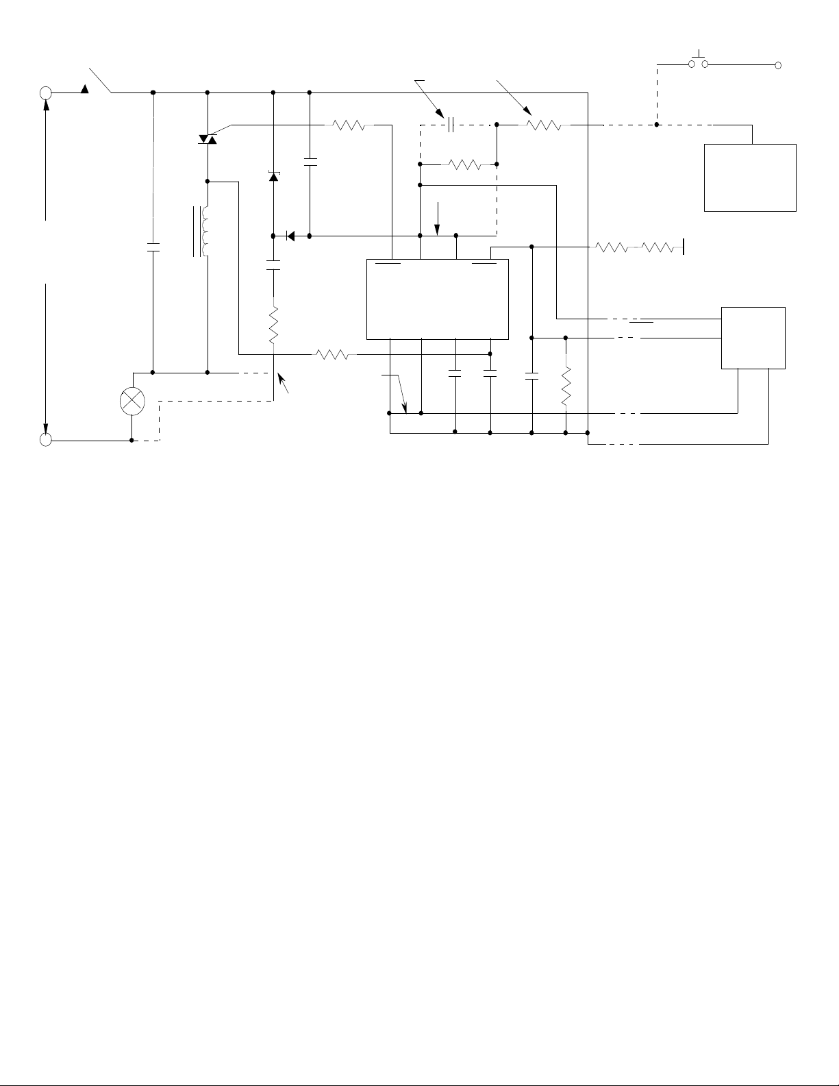
These functions may be implemented with very few interface components, as shown in Figure 5. When implemented in this manner, touching of the Touch Plate causes the lamp brightness to change as follows:
1.
If the Touch Plate is touched momentarily (42ms to
333ms), the lamp is:
a) turned off if it was on,
b) turned on if it was off.
The brightness resulting is either full brightness or
depending on the circuit type, a previous brightness
stored in the IC memory.
2. If the Touch Plate is touched for a prolonged time
(more than 342ms) the light intensity changes slowly.
As long as the touch is maintained, the change continues; the direction of change reverses whenever the
maximum or minimum brightness is reached.
April 1995
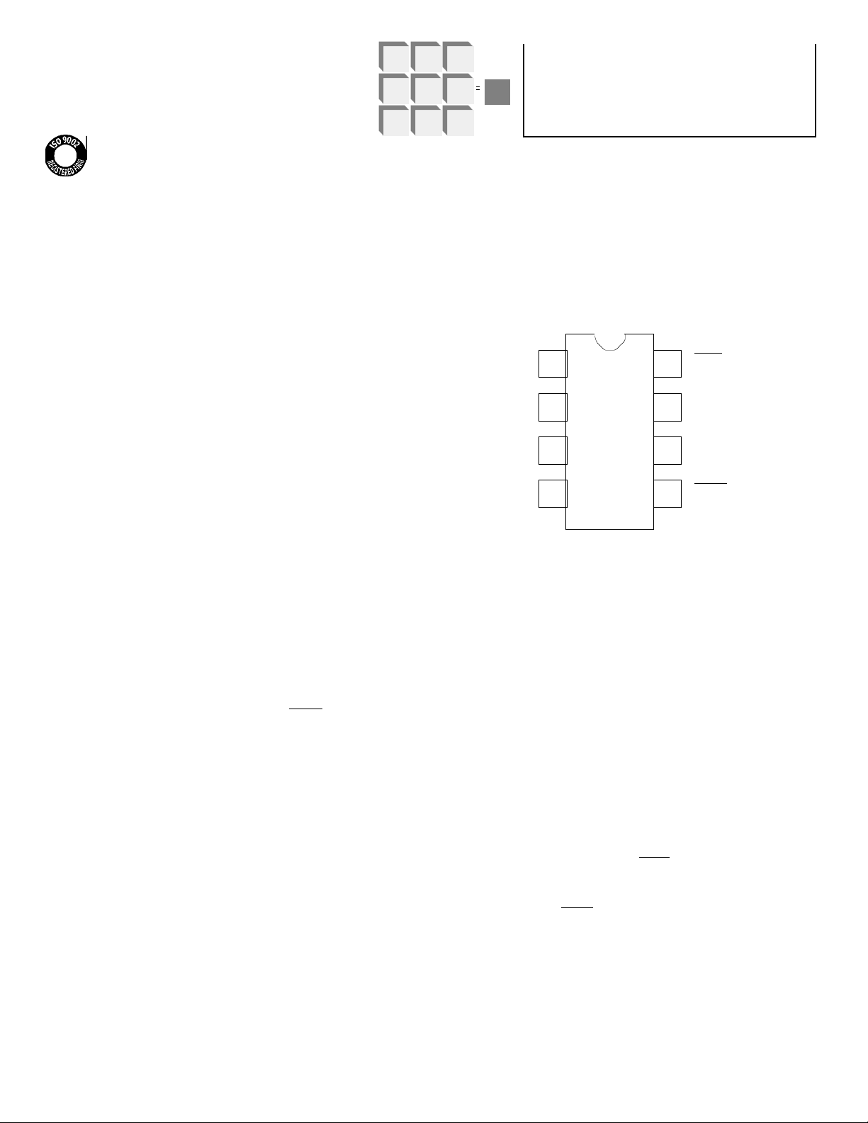
PIN ASSIGNMENT - TOP VIEW
STANDARD 8 PIN PLASTIC DIP
LSI
VSS(+V)
DOZE
CAP
SYNC
The IC also provides an input for slow dimming. By
applying a slow clock to this input, the lamp can be
dimmed slowly until total turn off occurs. This feature can be useful at bedtime in a child’s room.
INPUT/OUTPUT DESCRIPTION:
VSS (Pin 1)
Supply voltage positive terminal.
DOZE (Pin 2)
A clock applied to this input causes the brightness to decrease in equal increments with each negative transition
of the clock. Eventually, when the lamp turns off, this input has no further effect. The lamp can be turned on
again by activating either the SENS input or the EXT input. For the transition from maximum brightness to off, a
total of 83 clock pulses are needed at the DOZE input.
When either the SENS or the EXT input is active, the
DOZE input is disabled. (See Figure 7)
CAP (Pin 3)
The CAP input is for the PLL filter capacitor. A 0.047µF
capacitor should be connected to this input.
1
LS7231-34
2
3
4
FIGURE 1
8
7
6
5
TRIG
VDD (-V)
EXT
SENS
Page 2

TRIG (Pin 8)
The TRIG output is a low level pulse occurring once every
half-cycle of the SYNC input. The conduction angle, Ø, of the
output in relation to the SYNC signal controls the lamp brightness.
In continuous dimming operation (i.e. when the SENS input is
continuously held low) the TRIG conduction angle, Ø, sweeps
up and down between 41˚ and 158˚ continuously. The time vs
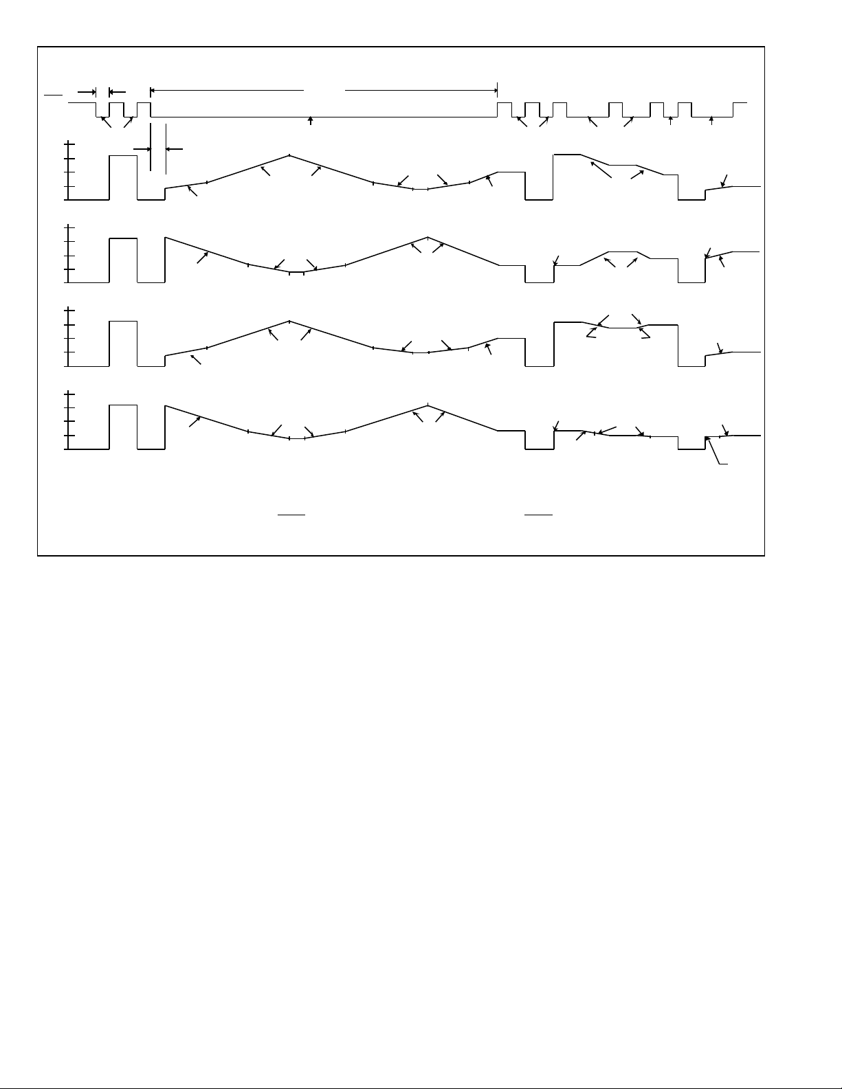
Ø curve is not linear (See Figure 2). Between two maxima on
this curve, there are 4 discontinuous points labeled A1, B1,
B2, A2. The discontinuities are as follows:
1. From maximum to A1. In this region, Ø is changed by
equal increments (∆ø) for every 2 SYNC clocks.
2. From A1 to B1. In this region, the increments (∆ø) take
place for every 4 SYNC clocks.
3. From B1 to B2. In this region Ø is held at a constant
level (∆ø = 0).
4. From B2 to A2. Same as 2.
5. From A2 to Max. Same as 1.
The slower rate of change in ø over A1B1B2A2 region is to
accommodate for eye adjustment at lower light intensity.
The functional differences of different versions of the light dimmer ICs are explained in Table 1 and the TRIG
output conduction angle diagrams in Figure 2.
PART
NUMBER
LS7231
LS7232
LS7233
LS7234
DIMMING
DIRECTION
REVERSAL
(Note 3)
N/A
N/A
NO
YES
N/A
YES
N/A
N/A
YES
NO
N/A
NO
NOTE 1: "Memory" refers to the conduction angle, Ø which existed prior to the current off-state. First time after power-up,
the Memory value defaults to maximum conduction angle.
NOTE 2: First time after power-up, LONG touch causes intensity to vary starting at minimum conduction angle.
NOTE 3: NO = Dimming direction does not reverse from prior dimming direction.
YES = Dimming direction does reverse from prior dimming direction.
N/A = Does not apply
TABLE 1
TOUCH TYPE
SHORT (TS1 Duration) LONG (TS2 Duration)
PRE-TOUCH POST-TOUCH PRE-TOUCH POST-TOUCH
Ø Ø Ø Ø
Off Max Off Starts varying at Min
Max Off Max Starts varying at Max
Intermediate Off Intermediate Starts varying at
Pre-Touch brightness
Off Memory Off Starts varying at
(Note 1) Memory (Note 2)
Max Off Max Starts varying at Max
Intermediate Off Intermediate Starts varying at
Pre-Touch brightness
Off Max Off Starts varying at Min
Max Off Max Starts varying at Max
Intermediate Off Intermediate Starts varying at
Pre-Touch brightness
Off Memory Off Starts varying at
(Note 1) Memory (Note 2)
Max Off Max Starts varying at Max
Intermediate Off Intermediate Starts varying at
Pre-Touch brightness
SYNC (Pin 4)
The AC Line Frequency is applied to this input through an
external RC circuit (See Figure 5). The Phase-Lock Loop
in the IC synchronizes all internal timings to the AC signal
at the SYNC input.
SENS (Pin 5)
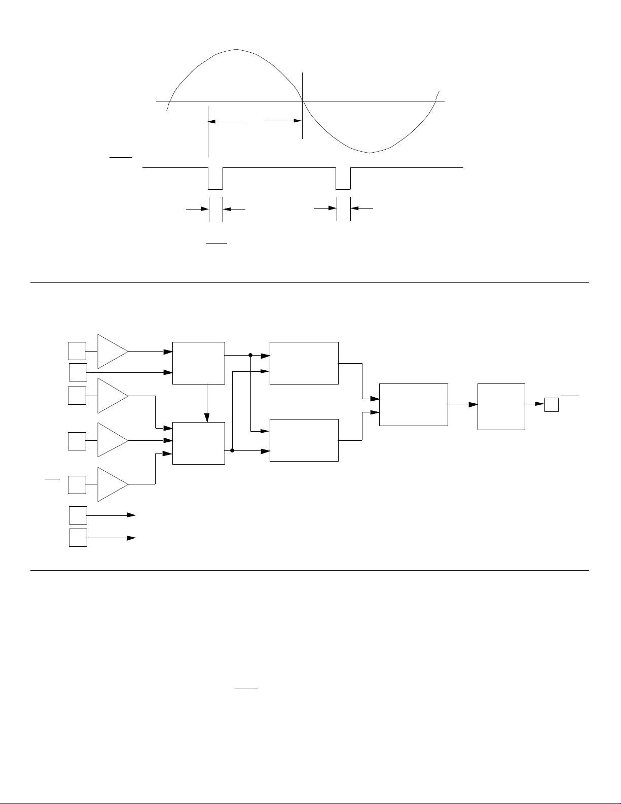
A low level activates this input (See Table 1) which controls the turn-on, turn-off and conduction angle Ø (SeeFigure 3) of the TRIG signal with respect to the SYNC input.
EXT (Pin 6)
The EXT input is functionally identical to the SENS input
except that a high level activates this input. It is recommended that the EXT input be used instead of the
SENS input when long extension wires are employed between the IC and the Sensing Circuitry (See Figure 5 and
Figure 6) because the EXT input is less susceptible to
“Noise”.
VDD (Pin 4)
Page 3

ABSOLUTE MAXIMUM RATINGS:
PARAMETER SYMBOL VALUE UNIT
DC Supply Voltage VSS +20 V
Any Input Voltage VIN VSS -20 to VSS + 0.5 V
Operating Temperature TA 0 to +80 ˚C
Storage Temperature TSTG -65 to +150 ˚C
DC ELECTRICAL CHARACTERISTICS:
(TA = 25˚C, all voltages referenced to VDD)
PARAMETER SYMBOL MIN TYP MAX UNIT CONDITION
Supply Voltage VSS +12 – +18 V -
Supply Current ISS – 1.0 1.4 mA VSS = +15V,
output off
Input Voltages:
DOZE LO VIZL 0 – VSS-6 V -
DOZE HI VIZH VSS-2 – VSS V -
SYNC LO VIRL 0 – VSS-9.5 V -
SYNC HI VIRH VSS-5.5 – VSS V -
SENS LO VIOL 0 – VSS-8 V -
SENS HI VIOH VSS-2 – VSS V -
EXT LO VIVL 0 – VSS-8 V -
EXT HI VIVH VSS-2 – VSS V -
Input Current:
SYNC, SENS, EXT HI IIH – – 110 µA With Series 1.5MΩ
Resistor to
115VAC Line
SYNC, SENS, EXT LO IIL – – 100 nA -
DOZE HI IIH – – 100 nA -
DOZE LO IIL – – 100 nA -
TRIG HI Voltage VOH – VSS – V -
TRIG LO Voltage VOL – VSS-8 – V VSS = +15V
TRIG Sink Current IOS 25 – – mA VSS = +15V
VOL = VSS-4V
TIMING CHARACTERISTICS (See Figures 2 and 3):
All timings are based on fs = 60Hz, unless otherwise specified. 50Hz timings are 1.2 times 60Hz timings.
PARAMETER SYMBOL MIN TYP MAX UNIT
SYNC Frequency fs 40 - 70 Hz
SHORT TOUCH TS1 42 - 333 ms
(ON/OFF Operation)
LONG TOUCH TS2 342 - infinite ms
(Dimming Operation)
DOZE Frequency - - - 500 Hz
TRIG Pulse Width TW - 33 - µs
TRIG Conduction-Angle Ø 41 - 158 degrees
(Note 1)
Ø Period (Max to Max in - - 7.64 - seconds
continuous dimming)
A1B1 = B2A2 duration - - 934 - ms
B1B2 Min. intensity dwell - - 500 - ms
NOTE 1.
In the circuit schematic shown in Figure 5, the SYNC input signal is delayed in phase with respect to the AC Line by
about 7°. This delay reduces the conduction angle, Ø with respect to the AC Line by 7° from the values shown above.
Page 4
SENS
SHORT
A1
MEMORY
MEMORY
TS1
TS2
LS7231
150°
100°
50°
OFF
LS7232
150°
100°
50°
OFF
LS7233
150°
100°
50°
OFF
LS7234
150°
100°
50°
OFF
SBA = 1.4° per four SYNC CYCLES, 15 steps total for A1 to B1 or B2 to A2
SAA = 1.4° per two SYNC CYCLES, 68 steps total for A0 to A1 or A2 to A0
341ms
B2
B2
A0
A2
SBA
A0
SAA
A2
SBA
SAA
SLOPE = SAA
A1
A1
FIGURE 2. TRIG OUTPUT CONDUCTION ANGLE, Ø, VS SENS INPUT
SAA
B1
A0
SBA
A0
LONG
B2B1
B2
SHORT
SLOPE = SBA
B1
A0
A2
A1
A2
SAA
SBA
B1
SAASBA
A2
B2
B2
A0
SAA
A2
SAA
SAA
LONG
SAA
SAA
SAA
REVERSE
A1
SBA
SHORT LONG
B1
B2
MEMORY
SBA
B2
B1
SBA
SAA
SBA
B2
MEMORY
7631-4-032795-4
Page 5
SYNC
TRIG
ø
SYNC
CAP
DOZE
EXT
SENS
TW
TW
FIGURE 3. TRIG OUTPUT CONDUCTION ANGLE, Ø
BUF
4
3
BUF
2
BUF
6
BUF
5
PHASE
LOCK
LOOP
CONTROL
LOGIC
Ø
MEMORY
Ø
POINTER
DIGITAL
COMPARATOR
OUTPUT
DRIVER
TRIG
8
FIGURE 4
VSS
VDD
1
7
(+V)
(-V)
LS7231-4 BLOCK DIAGRAM
APPLICATION EXAMPLE:
A typical implementation of a lamp dimmer circuit is shown in Fig. 5. Here the brightness of the lamp is set by touching the Touch Plate . The functions of different components are as follows:
• The 15V DC supply for the chip is provided by Z, D1, R1, C2 and C5.
• R2 and C4 generate the filtered signal for the SYNC input for synchronizing the internal PLL with the line
frequency.
• R3 and C7 act as a filter circuit for the electronic extension. If extensions are not used, the EXT input (Pin 6)
should be tied to VDD (Pin 7).
• R4, R5, R6 set up the sensitivity of the SENS input. C6 provides noise filtering.
• C3 is the filter capacitor for the internal PLL.
• R8 provides current limiting and isolation between the chip output and the triac gate.
• C1 and L are RF filter circuits.
In the case of momentary power failure, the circuit state remains unchanged for a period of up to 1 sec. For longer
power interruptions, the output is shut off.
Page 6
P
A
B
FIGURE 5. A Typical Lamp Dimmer
SEE NOTE 2
P
115VAC
OR
220VAC
N
LOAD
C1
MT1
MT2
NOTES
G
T
Z
L
D1
C2
R1
SEE NOTE 4
1) All circuits connected by broken lines are optional.
2) C7 is used only with electronic extension and R7 is used only with mechanical switch.
3) Connection between Pin 1 & Pin 2 should be broken when DOZE circuit is used.
4) Use Connection A when Neutral is not available. Use Connection B when Neutral is available.
5) Connection between Pin 6 & Pin 7 should be broken when EXT is used.
R8
+
C5
-
TRIG VDD EXT SENS
R2
SEE NOTE 3
VSS DOZE CAP SYNC
1 2 3 4
8 7 6 5
C7
R3
SEE NOTE 5
LS7231-4
C3 C4
R7
C6
R4
R6
EXTN
VDD
SENS
DZ
V SS
R5
TOUCH
PLATE
ELECTRONIC
EXTENSION
(FIG. 6)
DOZE
CIRCUIT
(FIG. 7)
115V
(1)
C1 = 0.15µF,200V R4 = 1MΩ to 5MΩ,1/4W
C2 = 0.33µF,200V (Select for sensitivity)
C3 = 0.047µF,25V R5, R6 = 2.7MΩ,1/4W
C4 = 470pF,25V R7 = 150KΩ,1/4W
C5 = 47µF,25V R8 = 100Ω,1/4W
C6 = 680pF,25V D1 = IN4148
(2)
C7 = 0.1µF,25V Z = 15V,1W (Zener)
R1 = 270Ω,1W T = Q4006L4 Triac (Typical)
R2 = 1.5MΩ,1/4W L = 100µH (RFI Filter)
R3 = 1.5MΩ,1/4W
(1) For Connection A. Use 0.22µF for Connection B.
(2) For Connection A. Use 1/4W for Connection B.
220V
C1 = 0.15µF, 400V R4 = 1MΩ to 5MΩ,1/4W
(3)
C2 = 0.22µF, 400V (Select for sensitivity)
C3 = 0.047µF, 25V R5, R6 = 4.7MΩ,1/4W
C4 = 470pF, 25V R7 = 150KΩ,1/4W
C5 = 47µF, 25V R8 = 100Ω,1/4W
C6 = 680pF,25V D1 = 1N4148
C7 = 0.1µF, 25V Z = 15V,1W (Zener)
(4)
R1 = 1KΩ, 2W T = Q5004L4 Triac (Typical)
R2 = 1.5MΩ,1/4W L = 200µH (RFI Filter)
R3 = 1.5MΩ,1/4W
(3) For Connection A. Use 0.1µF for Connection B.
Page 7
TOUCH PLATE
*R
2KΩ,1/4W
EXTN
IN914
MPS8599
200KΩ,1/4W
*R
*R = 2MΩ,1/4W for 115VAC
*R = 3.6MΩ,1/4W for 220VAC
P
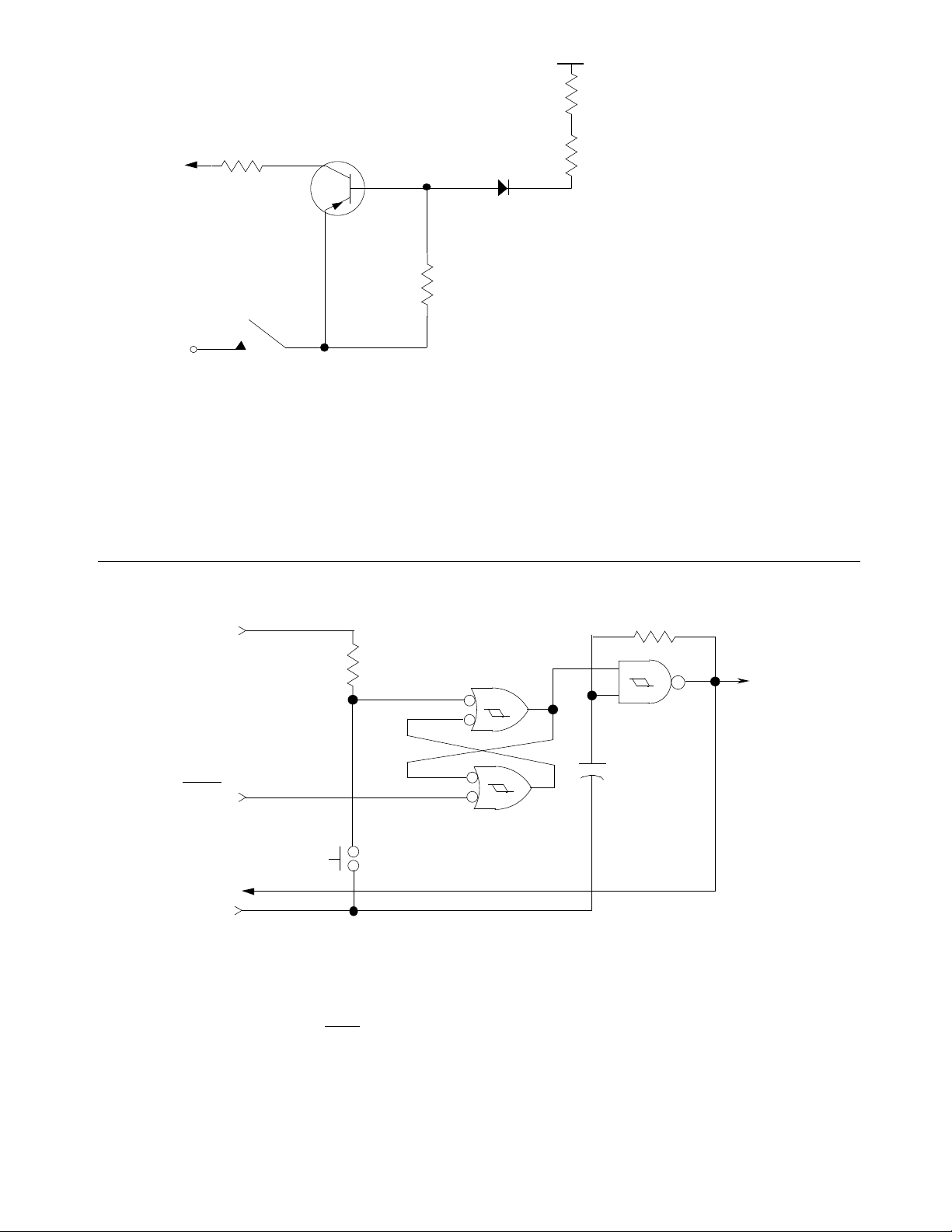
FIGURE 6. ELECTRONIC EXTENSION
EXTENSIONS:
All switching and dimming functions can also be implemented by utilizing the EXT input. This can be
done by either a mechanical switch or the electronic switch in conjunction with a Touch Plate as shown in
Figure 6. When the plate is touched, a logic high level is generated at the EXT input of the IC for both
half- cycles of the line frequency. (See Figure 5)
VSS
SENS
VDD
DZ
3.3MΩ,1/4W
DOZE
SWITCH
FIGURE 7. DOZE CIRCUIT
U1-1
U1-2
3.3MΩ,1/4W
DZ
U1-3
+
10µF
-
U1 = CD4093
DOZE CIRCUIT:
The DOZE circuit shown in Figure 7 generates a slow clock (0.04Hz) at the DZ terminal. If the Touch Plate
(Figure 5) is not touched, the SENS terminal of the DOZE circuit of Figure 7 sits at a logic high level. A momentary pressing of the DOZE switch sets the SR flip-flop, enabling the oscillator. Every negative transition
of the clock (DZ terminal) causes the light intensity to be reduced by equal increments, until eventually the
light is shut off. The oscillator has no further effect on the dimmer circuit. When the light is turned on again
by touching theTouch Plate, the SR flip-flop is reset and the DZ clock is turned off.
When the DOZE circuit is used, the connection between DOZE input (Pin 2) and VSS (Pin 1) as shown in
Figure 5, should be removed.
Page 8
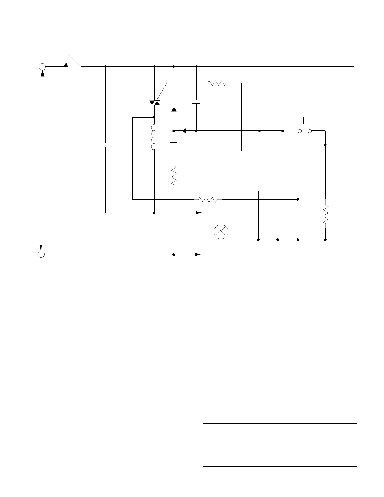
FIGURE 8. A SWITCH-OPERATED LAMP DIMMER
APPLICATIONS:
1. Foot-Switch Dimmer for large floor lamps.
2. Hand-Switch Dimmer for end-table lamps.
AC ON-OFF SWITCH
115VAC
OR
220VAC
(SEE NOTE)
C1
MT1
MT2
G
R3
+
T1
Z1
C5
-
PUSHBUTTON
SWITCH
D1
L
C2
8 7 6 5
TRIG VDD EXT SENS
R1
LS7231-4
VSS DOZE CAP SYNC
R2
1 2 3 4
C3
C4
R4
OUT
TO
LAMP
NOTE: Operation is independent of Line Plug Polarity
115V 220V
C1 = 0.15µF,200V C1 = 0.15µF,400V
C2 = 0.22µF,200V C2 = 0.1µF,400V
C3 = .047µF,25V C3 = .047µF,25V
C4 = 470pF,25V C4 = 470pF,25V
C5 = 47µF,25V C5 = 47µF,25V
R1 = 270 Ω,1/4W R1 = 1KΩ,1/4W
R2 = 1.5M Ω,1/4W R2 = 1.5MΩ,1/4W
R3 = 100 Ω,1/4W R3 = 100Ω,1/4W
R4 = 1M Ω,1/4W R4 = 1MΩ,1/4W
D1 = IN4148 D1 = IN4148
Z1 = 15V,1W (Zener) Z1 = 15V,1W (Zener)
T1 = Q4008L4 (Typical) T1 = Q5004L4 (Typical)
L = 100µH (RFI Filter) L = 200µH (RFI Filter)
The information included herein is believed to be
accurate and reliable. However, LSI Computer Systems,
Inc. assumes no responsibilities for inaccuracies, nor for
any infringements of patent rights of others which may
result from its use.
 Loading...