

Page 1
LSI/CSI
LSI Computer Systems, Inc. 1235 Walt Whitman Road, Melville, NY 11747 (516) 271-0400 FAX (516) 271-0405
LS7211-7212
U
®
L
A3800
PROGRAMMABLE DIGITAL DELAY TIMER
FEATURES:
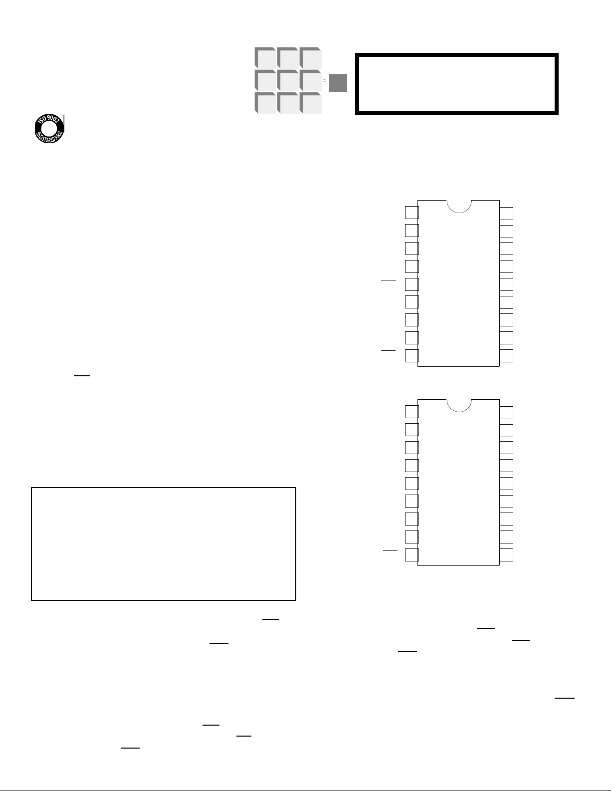
PIN ASSIGNMENT - TOP VIEW
• 8-bit programmable delay from nanoseconds to days
• On chip oscillator (RC or Crystal) or external clock time base
• Selectable prescaler for real time delay generation based
on 50Hz/60Hz time base or 32.768KHz watch crystal
• Four operating modes
• Reset input for delay abort
• Low quiescent and operating current
• Direct relay drive
• +4V to +18V operation (VDD-VSS)
• 18-pin plastic DIP or SOIC package
DESCRIPTION:
The LS7211/LS7212 are monolithic CMOS integrated circuits for generating digitally programmable delays. The delay is controlled by 8 binary weighted inputs, WB0-WB7, in
conjunction with an applied clock or oscillator frequency.
VDD (+V)
RC/CLOCK
RCS/CLKS
PSCLS
RESET
VSS (-V)
OUT
LSI
1
A
2
B
3
LS7211
4
5
6
7
8
9
The programmed time delay manifests itself in the Delay
Output (OUT) as a function of the Operating Mode selected
by the Mode Select inputs A and B: One-Shot, Delayed
Operate, Delayed Release or Dual Delay. The time delay is
initiated by a transition of the Trigger Input (TRIG).
I/O DESCRIPTION:
MODE SELECT Inputs (A &B, Pins 1 & 2)
The 4 operating modes are selected by Inputs A and B
according to Table 1
TABLE 1. MODE SELECTION
A B MODE
0 0 One-Shot (OS)
0 1 Delayed Operate (DO)
1 0 Delayed Release (DR)
VDD (+V)
XTLI/CLOCK
XTLO
PSCLS
RESET
VSS (-V)
OUT
LSI
A
1
2
B
3
LS7212
4
5
6
7
8
9
1 1 Dual Delay (DD)
FIGURE 1
Each input has an internal pull-up resistor of about 500KΩ.
18
17
16
15
14
13
12
11
10
18
17
16
15
14
13
12
11
10
June 1997
TRIG
WB0
WB1
WB2
WB3
WB4
WB5
WB6
WB7
TRIG
WB0
WB1
WB2
WB3
WB4
WB5
WB6
WB7
One-Shot Mode (OS)
A positive transition at the TRIG input causes OUT to
switch low without delay and starts the delay timer. At the
end of the programmed delay timeout, OUT switches high.
If a delay timeout is in progress when a positive transition
occurs at the TRIG input, the delay timer will be restarted.
A negative transition at the TRIG input has no effect.
Delayed Operate Mode (DO)
A positive transition at the TRIG input starts the delay timer. At the end of the delay timeout, OUT switches low. A
negative transition at the TRIG input causes OUT to switch
high without delay. OUT is high when TRIG is low.
Delayed Release Mode (DR)
A negative transition at the TRIG input starts the delay timer. At the end of the delay timeout, OUT switches high. A
postive transition at the TRIG input causes OUT to switch
low without delay. OUT is low when TRIG is high.
Dual Delay Mode (DD)
A positive or negative transition at the TRIG input starts
the delay timer. At the end of the delay timeout, OUT
switches to the logic state which is the inverse of the TRIG
input. If a delay timeout is in progress when a transition
occurs at the TRIG input, the delay timer is restarted.
Page 2
TRIGGER Input (TRIG, Pin 18)
A transition at the TRIG input causes OUT to switch with or
without delay, depending on the selected mode. The TRIG
input to OUT transition relation is always opposite in polarity, with the exception of One-Shot mode. (See Mode
definitions above.) TRIG input has an internal pull-down resistor of about 500KΩ and is buffered by a Schmitt trigger
to provide input hysterisis.
LS7211 TIME BASE Input (RC/CLOCK, Pin 4)
For LS7211, the basic timing signal is applied at the RC/
CLOCK input. The clock can be provided from either an external source or generated by an internal oscillator by connecting an R-C network to this input.
The frequency of oscillation is given by ƒ ≈ 1/RC. Chip-tochip oscillation tolerance is ± 5% for a fixed value of RC.
The minimum resistance, R MIN = 4000Ω, VDD = + 4V
= 1200Ω, VDD = +10V
= 600Ω, VDD = +18V
The external clock mode is selected by applying a logic low
to the RCS/CLKS input (Pin 5); the internal oscillator mode
is selected by applying a high level to the RCS/CLKS input.
LS7212 TIME BASE Input (XTLI/CLOCK, Pin 4)
For LS7212, the basic timing clock is applied to the XLTI/
CLOCK input from either an external clock source or generated by an internal crystal oscillator by connecting a crystal
between XTLI/CLOCK input and the XTLO output (Pin 5).
TIMER RESET Input (RESET, Pin 7)
When RESET input switches high, any timeout in progress
is aborted and OUT switches high without delay. With RESET high, OUT remains high. When RESET switches low
with TRIG low in any mode, OUT remains high. When RESET switches low with TRIG high in Delayed Operate and
Dual Delay modes, the delay timer is started and OUT
switches low at the end of the delay timeout. When RESET switches low with TRIG high in Delayed Release
mode, OUT switches low without delay. When RESET
switches low with TRIG high in One-Shot mode, OUT remains high. RESET input has an internal pull-down resistor
of about 500KΩ.
VSS (-V, Pin 8)
Supply voltage negative terminal or GND.
DELAY Output (OUT, Pin 9)
Except in One-Shot mode, OUT switches with or without
delay (depending on mode) in inverse relation to the logic
level of the TRIG input. In One-Shot mode, a timed low
level is produced at OUT, in response to a positive transition of the TRIG input.
WEIGHTING BIT Inputs (WB7 To WB0, Pins 10 - 17)
Inputs WB0 through WB7 are binary weighted delay bits
used to program the delay according to the following
relations:
LS7211 TIME BASE SELECT Input (RCS/CLKS, Pin 5)
For LS7211, the external clock operation at Pin 4 is selected by applying a logic low to the RCS/CLKS input. The
internal oscillator option with RC timer at Pin 4 is selected
by applying a logic high at the RCS/CLKS input. RCS/CLKS
input has an internal pull-down resistor of about 500KΩ.
LS7212 TIME BASE Output (XTLO, Pin 5)
For LS7212, when a crystal is used for generating the time
base oscillation, the crystal is connected between XTLI/
CLOCK and XTLO pins.
PRESCALER SELECT Input (PSCLS, Pin 6)
The PSCLS input is a 3-state input, which selects one of
three prescale factors according to Table 2.
TABLE 2. PRESCALE FACTOR SELECTION
PSCLS Input S (Prescale Factor )
Logic Level LS7211 LS7212
Float 1 1
Low 3000 32768
High 3600 32768x60
Using prescale factors of 3000 and 3600, delays in units of
minutes can be produced from 50Hz and 60Hz line sources. Prescale factors of 32,768 and 32,768 x 60 can be used
to generate accurate delays in units of seconds and minutes, respectively, from a 32KHz watch crystal.
One-Shot Mode: Pulse width = SW
ƒ
All other Modes: Delay = SW + .5
ƒ
Where:
S = Prescale factor (See Table 2)
ƒ = Time base frequency at Pin 4
W = WB0 + WB1 + ....... WB7
The weighting factor W is calculated by substituting in the
equation above for W, the weighted values for all the WB
inputs that are at logic high. The weighted values for the
WB inputs are shown in Table 3. Each WB input has an internal pull-down resistor of about 500KΩ.
TABLE 3. BIT WEIGHTS
BITS VALUE
WB0 1
WB1 2
WB2 4
WB3 8
WB4 16
WB5 32
WB6 64
WB7 128
VDD (+V, Pin 3)
Supply voltage positive terminal.
Page 3
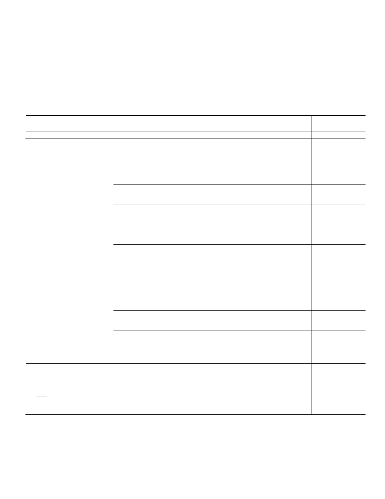
ABSOLUTE MAXIMUM RATINGS: (All voltages referenced to VSS)
ELECTRICAL CHARACTERISTICS (Voltages referenced to Vss)
SYMBOL VALUE UNIT
DC Supply Voltage VDD +19 V
Voltage (Any Pin) VIN VSS-.3 to VDD+.3 V
Operating Temperature TA -20 to +85 °C
Storage Temperature TSTG -65 to +150 °C
Characteristic SYMBOL VDD Unit Condition
Supply Voltage VDD - 4.0 18.0 4.0 18.0 4.0 18.0 V -
4.0 32 - 27 - 20 - µA
Supply Current IDD 10.0 190 - 160 - 110 - µA with the clock off
18.0 560 - 437 - 330 - µA
Input Voltages:
4.0 - 1.0 - 1.0 - 1.0 V
Trigger Low VTL 10.0 - 3.0 - 3.0 - 3.0 V -
18.0 - 5.8 - 5.8 - 5.8 V
4.0 3.0 - 3.0 - 3.0 - V
Trigger High VTH 10.0 6.6 - 6.6 - 6.6 - V -
18.0 11.0 - 11.0 - 11.0 - V
4.0 1.5 - 1.5 - 1.5 - V
Trigger Hysteresis 10.0 3.0 - 3.0 - 3.0 - V -
18.0 4.8 - 4.8 - 4.8 - V
4.0 - 1.2 - 1.2 - 1.2 V
All other inputs, Low VIL 10.0 - 4.1 - 4.1 - 4.1 V -
18.0 - 7.2 - 7.2 - 7.2 V
4.0 2.1 - 2.1 - 2.1 - V
All other inputs, High VIH 10.0 5.3 - 5.3 - 5.3 - V -
18.0 9.3 - 9.3 - 9.3 - V
Input Currents:
4.0 - 2.6 - 2.0 - 1.5 µA
PSCLS Low IPL 10.0 - 22.0 - 17.0 - 13.0 µA Input at VSS
18.0 - 70.0 - 54.0 - 41.0 µA
4.0 - 5.8 - 4.4 - 3.4 µA
PSCLS High IPH 10.0 - 26.0 - 20.0 - 15.2 µA Input at VDD
18.0 - 82.0 - 63.0 - 48.0 µA
4.0 - 2.0 - 1.6 - 1.3 µA
A, B Low IML 10.0 - 37.0 - 28.0 - 22.0 µA Input at VSS
18.0 - 132.0 - 101.0 - 77.0 µA
A, B High IMH - - 100 - 100 - 200 nA Input at VDD
All other inputs, Low IIL - - 100 - 100 - 200 nA Input at VSS
4.0 - 4.6 - 3.5 - 2.7 µA
All other inputs, High IIH 10.0 - 33.0 - 25.0 - 19.0 µA Input at VDD
18.0 - 121.0 - 93.0 - 71.0 µA
Output Current:
4.0 23.0 - 18.0 - 13.0 - mA
OUT Sink IOSNK 10.0 43.0 - 33.0 - 25.0 - mA Vo = +0.5V
18.0 56.0 - 43.0 - 32.0 - mA
4.0 2.6 - 2.0 - 1.5 - mA
OUT Source IOSRC 10.0 7.8 - 6.0 - 4.5 - mA Vo = VDD-.5V
18.0 11.5 - 8.8 - 6.5 - mA
-20°C +25°C +85°C
Min Max Min Max Min Max
Page 4
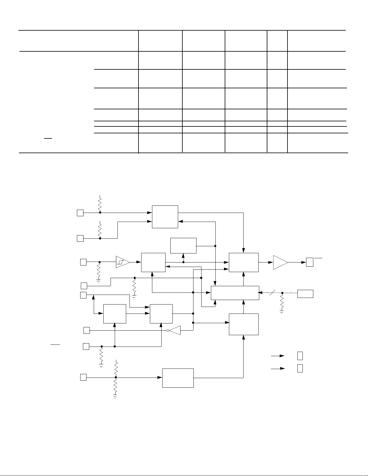
ELECTRICAL CHARACTERISTICS (Voltages referenced to Vss) (Con’t)
Characteristic SYMBOL VDD Unit Condition
Min Max Min Max Min Max
Switching Characteristics (See Fig. 3)
4.0 - 1.3 - 1.0 - 0.76 MHz
RC Oscillator Frequency fosc 10.0 - 4.0 - 3.0 - 2.3 MHz -
18.0 - 6.0 - 4.5 - 3.4 MHz
4.0 - 2.3 - 1.8 - 1.3 MHz For prescale
External Clock or fext 10.0 - 7.0 - 5.5 - 4.0 MHz factor S = 1 or 3000
Crystal Oscillator 18.0 - 11.0 - 8.5 - 6.5 MHz or 3600
Frequency 4.0 - 1.2 - 0.93 - 0.7 MHz S = 32768
fext 10.0 - 4.0 - 3.0 - 2.3 MHz or
18.0 - 7.0 - 5.5 - 4.2 MHz 32768 X 60
TRIG Set-Up Time t1 - 23 - 30 - 40 - ns A, B Set-Up Time t2 - 0 - 0 - 0 - ns WB0 - WB7 Set-Up Time t3 - 0 - 0 - 0 - ns -
4.0 215 - 280 - 370 - ns
Clock to Out Delay t4 10.0 80 - 105 - 140 - ns CL = 50pF
18.0 50 - 65 - 85 - ns
+V
A 1
TRIG 18
CLOCK/RC/XTLI
XTLO(LS7212)
RCS/CLKS(LS7211)
2B
7RESET
4
5
5
500KΩ
6PSCLS
500KΩ
+
V
500KΩ
500KΩ
OSC
+V
1MΩ
1MΩ
500K
Ω
LATCH
MODE
REG
CLOCK
MUX
EDGE
DETECT
3-STATE
DECODER
CONTROL
LOGIC
LATCH/TIMER
PRESCALER
+V
-V (Gnd)
8
BUF
500KΩ (8)
10-17
VDD
3
8
VSS
9
OUT
WB7-WB0
FIGURE 2. LS7211/LS7212 BLOCK DIAGRAM
Page 5
t0
Clock
TRIG
A,B
t3
WB0-WB7
OUT
t1
t2
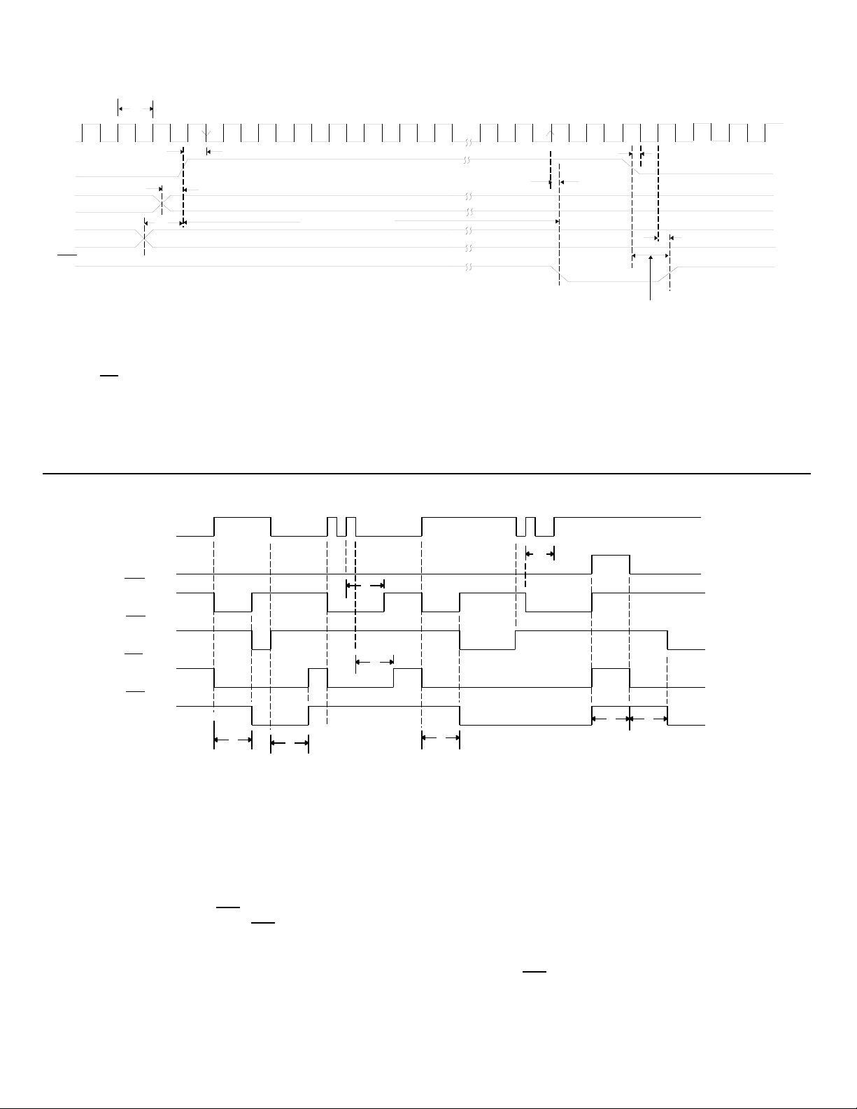
A = 0, B = 1, Delayed Operate
Programmed Delay
t1
t4
t4
Immediate Release
Note 1. TRIG in put is clocked in by the negative edge of external clock.
Note 2. Inputs A, B and WB0 - WB7 are sampled only at a TRIG input trainsition and ignored at all other times.
Note 3. OUT is switched by the positive edge of the external clock.
FIGURE 3. INPUT/OUTPUT TIMING
TRIG
RESET
OUT(OS)
C
F
OUT(DO)
OUT(DR)
OUT(DD)
A
B
D
G H
E
A. Turn-on delay in DO and DD modes; Pulse-width in OS mode.
B. Turn-off delay in DR and DD modes.
C. Pulse-width extended by re-trigger in OS mode. No effect in DO and DD modes because TRIG switches back low
before turn-on delay has timed out.
D. Turn-off delay in DR mode.
E. Turn-on delay in DO and DD modes; pulse-width in OS mode.
F. No effect in DO, DR and DD modes because of TRIG’s switching back to opposite levels.
G. Time-outs aborted and OUT forces high by RESET.
H. After the removal of RESET, OUT switches to the inverse polarity of TRIG immediately (DR) or after the timeout
(DO,DD). No effect in OS.
FIGURE 4. MODE ILLUSTRATION WITH TRIG, OUT AND RESET
Page 6
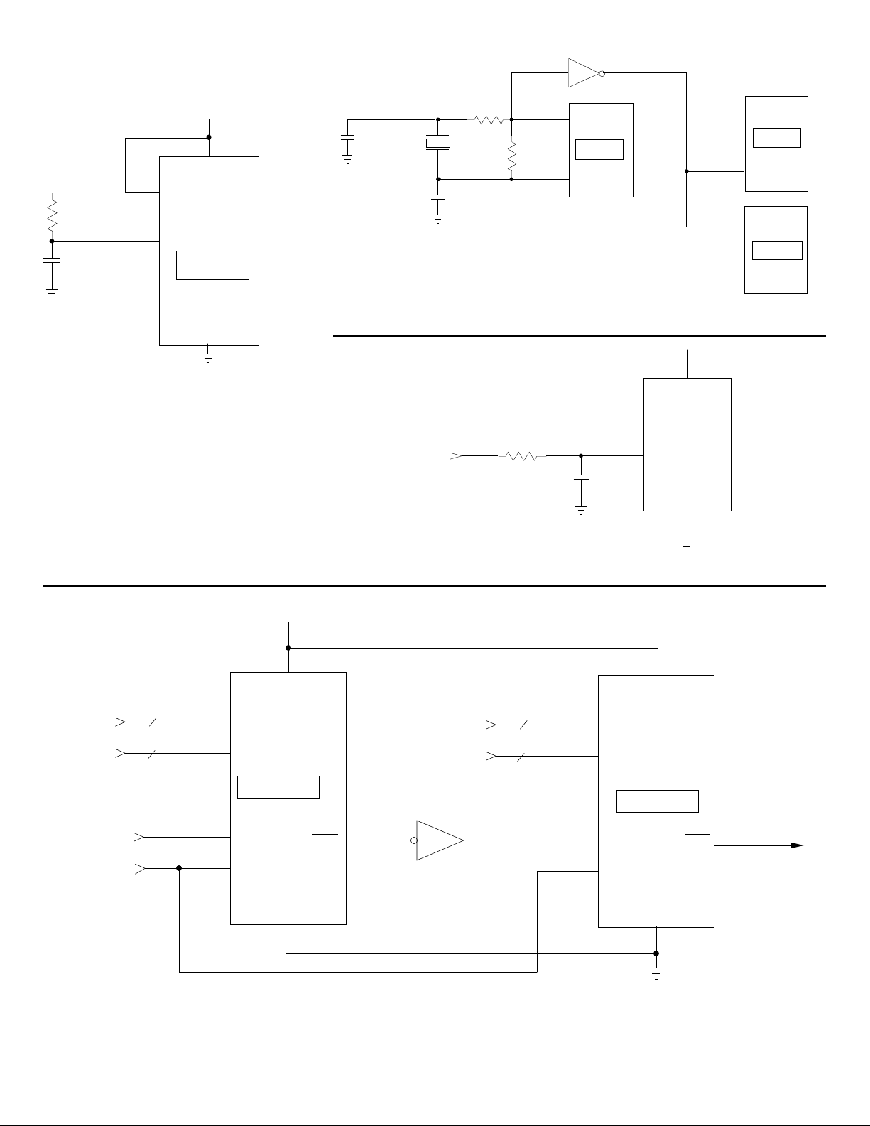
+V
FIGURE 5. RC-Oscillator Connection
10 X 10 X .1 X 10
1M
10K Ω
.1µF
ƒ =
ƒ
5
RCS/CLKS
4
RC
LS7211
1
3 -6
+V
3
VDD
VSS
8
= 1KHz
470KΩ
25pF
FIGURE 6. MULTI-TIMER WITH SINGLE CRYSTAL TIME-BASE
120VAC
CRYSTAL
25pF
10M Ω
5
4
XTLO
LS7212
XTLI
200pF
4
CLOCK
4
4
CLOCK
+V
3
VDD
LS7211
VSS
8
LS7211
CLOCK
LS7212
*
*
TRIGGER
FIGURE 7. DRIVING CLOCK INPUT FROM THE AC LINE
+V
3
VDD
10-17
8
2
WB0-WB7
1,2
A,B
*
2
8
10-17
1,2
*
3
VDD
WB0-WB7
A,B
LS7211
LS7211
18
TRIG
ƒ
4
CLOCK
9
OUT
Vss
8
18
4
TRIG
CLOCK
8
Vss
OUT
OUT
9
* Connect for desired delay and mode
FIGURE 8. DELAY EXTENSION BY CASCADING
Page 7
TRIGGER IN
25pF
25pF
ƒ
470K Ω
+V
S1
18
10M Ω
1
2
4
5
6
A
B
TRIG
XTLI
XTLO
PSCLS
VDD
WB0
WB1
WB2
WB3
WB4
WB5
WB6
WB7
17
16
15
14
13
12
11
10
+V
3
1s/1m
2s/2m
4s/4m
8s/8m
16s/16m
32s/32m
64s/64m
128s/128m
LS7212
7
8
9
RESET
Vss
OUT
+V
OUTPUT
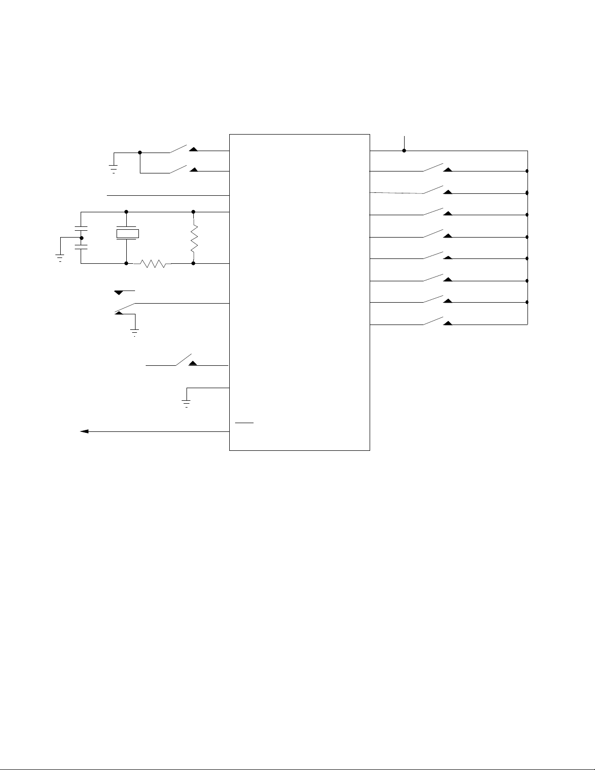
NOTE : Crystal Frequency, ƒ = 32,768Hz
Switch: S1 low: Delay increment = 1s; Maximum Delay = 255s
S1 high: Delay increment = 1m; Maximum Delay = 255m
s = seconds
m = minutes
FIGURE 9. PROGRAMMABLE ACCURATE REAL-TIME DELAY GENERATION
Page 8
TRIG
+V
DD
3
1
A
2
B
ƒi
+V
ƒo
4
CLOCK
7
RESET
18
9
OUT
V
LS7212
Vss
WB0
17
16
WB1
15
WB2
14
WB3
13
WB4
12
WB5
11
WB6
10
WB7
8
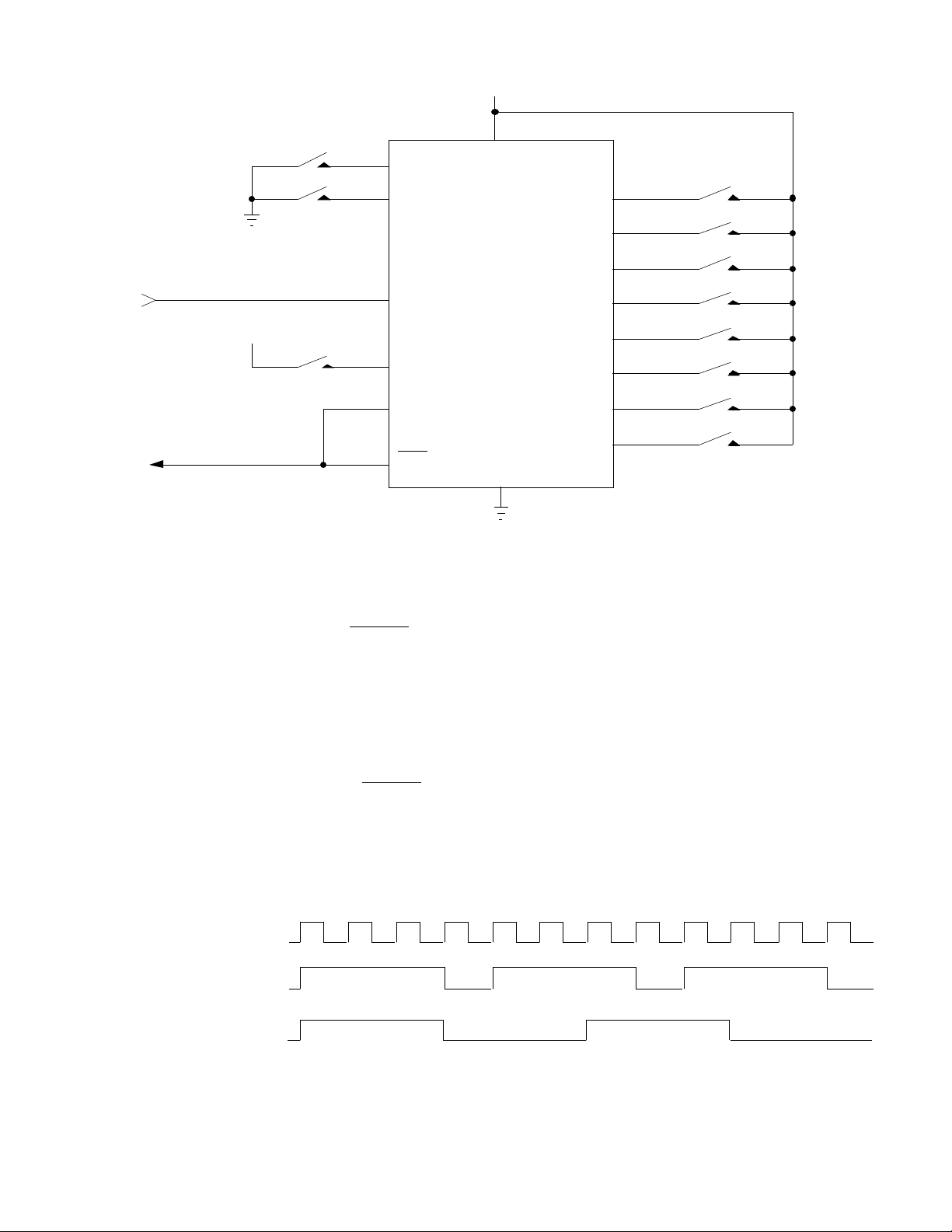
CASE 1. MODE = DO or DR; PRESCALE FACTOR, S = 1
In this setup a frequency division of the input clock, ƒi by a factor of 2 to 257, in increments of 1 can be
obtained according to the equation:
ƒo =
The ƒo pulse width is non-symmetrical (non-50% duty -cycle)
CASE 2. MODE = DD; PRESCALE FACTOR, S = 1
In this setup a frequency division of the input clock, ƒi by a factor of 2 to 512, in increments of 2 can be
obtained according to the equation:
ƒo =
The ƒo pulse widths are symmetrical with 50% duty -cycle
EXAMPLES OF CASE 1 and CASE 2 FREQUENCY DIVISIONS WITH W = 2
ƒi
ƒo
Case 1, Mode = DO; ÷4
ƒi
W + 2
ƒi
2(W + 1)
where W (weighting factor) = 0 to 255
where W (weighting factor) = 0 to 255
ƒo
Case 2, Mode = DD; ÷6
FIGURE 10. PROGRAMMABLE FREQUENCY DIVIDER
 Loading...