

Page 1
PROGRAMMABLE DIGITAL DELAY TIMER
February 1998
FEATURES:
• Programmable Delay from 6 ms to "Infinity"
• Can be Cascaded for Sequential Events or Extended Delay
• +4.75V to +15V Operation (Vss -V
DD)
• On Chip Oscillator or External Clock time base
• High Noise Immunity
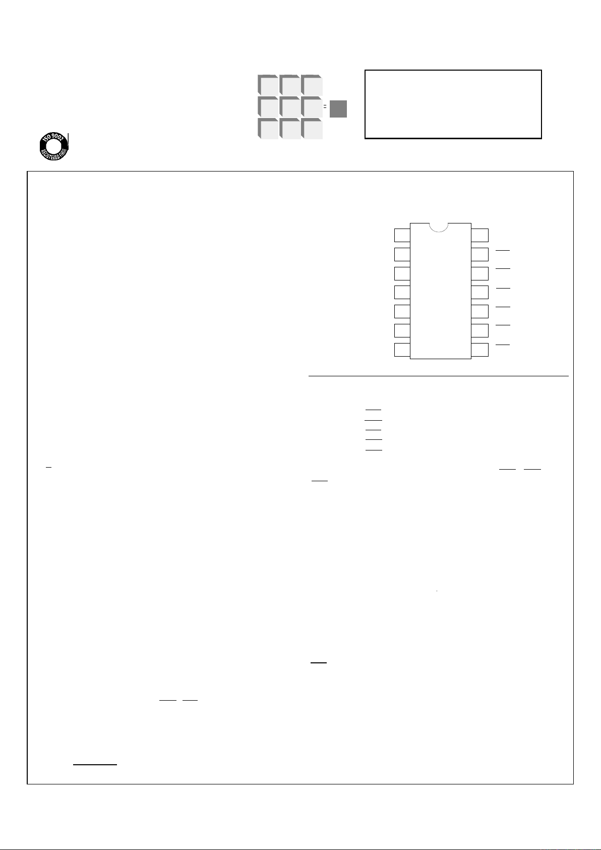
• LS7210 (DIP), LS7210-S (SOIC)-See Figure 1
DESCRIPTION:
The LS7210 is a monolithic MOS integrated circuit programmable
digital timer that can generate a delay in the range of 6ms to infinity.
The delay is programmed by 5 binary weighted input bits in combination with the time base provided. The chip can be operated in four
different modes: Delayed Operate, Delayed Release, Dual Delay
and One Shot. These modes are selected by the control inputs A
and B.
INPUT/OUTPUT DESCRIPTION:
OSCILLATOR Input (Pin 5)
The frequency of the internal oscillator is set by an RC network connected to the OSC input, as shown in Figure 2. The nominal oscillator frequency, f, at room temperature is given by f≈1/RC where R
values range from a minimum of 47KΩ to a maximum 3MΩ.
NOTE: Oscillation accuracy from chip to chip for a fixed value of RC,
is +
10%. (Parts can supplied to tighter tolerances.)
EXTERNAL CLOCK Input (Pin 6)
If the internal oscillator is not used, the chip can be driven by an external clock applied to this input.
CLOCK SELECT Input (Pin 4)
The internal oscillator or the external clock is selected by the proper
logic level applied to this input. A logic 1 selects the external clock
and logic 0 selects the internal oscillator. (See Note 1)
TRIGGER Input (Pin 3)
A positive or a negative transition at the trigger input initiates a delay
in turning on or off the output. A negative transition always turns on
the output with or without delay depending on the selected mode. A
positive transition at the trigger input always turns off the output (with
the exception of one-shot mode) with or without delay depending on
the selected mode. The delay is a function of the time base frequency and the weighting factor programmed at the weighting bit inputs. The trigger input is clocked into the input latch with the negative edge of the selected time base clock. All timings begin after the
latch has been set up. (See Note 1)
WEIGHTING FACTOR Inputs, WB0-WB4 (Pins 12-8)
A delay from the trigger input to the output is programmed by applying 1's complement binary weighted numbers at these 5 inputs.
(See Note 1) The exact equation for the delay is:
Delay =
(1 + 1, 023N) f = Oscillation Frequency
f N = Weighting Factor
TABLE 1. WEIGHTING BITS ASSIGNMENTS
INPUTS VALUE
WB0 1
WB1 2
WB2 4
WB3 8
WB4 16
Example: For a weighting factor of 25, inputs WB4, WB3, and
WB0 should be programmed to logic 0.
MODE SELECT Inputs A, B (Pins 2, 1)
The chip can be programmed to operate in four different modes
by applying the logic levels to inputs A and B as indicated in
Table 2. The mode select inputs are clocked into the input latches with the negative edge of the time base clock. These inputs
should not be changed while a delay timing is in progress. (See
Note 1)
TABLE 2. MODE SELECTION
CONTROL MODE
A B
1 1 Dual Delay
1 0 Delayed Release
0 1 Delayed Operate
0 0 One Shot
OUT Output (Pin 13)
The output is an open drain FET. To obtain proper switching of
the output between Logic 0 and 1 levels, an external pull down resistor to V
DD must be used. If the output is used only as a current
source, no such pull down is needed. The output is logically inverted with respect to the trigger input.
V
SS, VDD (Pins 14, 9)
Supply voltage positive, negative terminals.
NOTE 1: These inputs have internal pullup resistors.
1
2
3
4
5
6
7
14
LSI
13
12
11
10
9
8
LS7210
B
A
TRIGGER
CLOCK SELECT
OSCILLATOR
EXTERNAL CLOCK
V
DD
(-V)
V
SS
(+V)
OUT
WB0
WB1
WB2
WB3
WB4
FIGURE 1
PIN ASSIGNMENT - TOP VIEW
7210-041700-1
LSI/CSI
LSI Computer Systems, Inc. 1235 Walt Whitman Road, Melville, NY 11747 (631) 271-0400 FAX (631) 271-0405
LS7210
U
L
®
A3800
Page 2

7210-020298-2
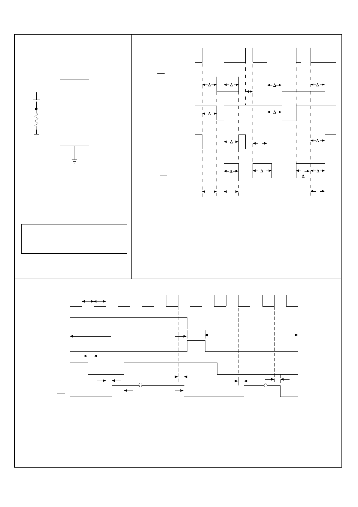
DELAYED RELEASE MODE
This mode causes a retriggerable delay in turning off the output
whenever there is a positive transition at the trigger input. The output is turned on without delay in response to a negative transition at
the trigger input.
ONE-SHOT MODE
In this mode, the chip functions like a retriggerable monostable
multi-vibrator. The output is turned on whenever there is a negative
transition at the trigger input. At the end of the programmed delay,
the output is turned off automatically. If there is a negative transition
at the trigger input before the delay is over, the delay is restarted.
A positive transition at the trigger input has no effect on the output
in this mode. NOTE: In One-Shot mode, the TRIGGER input must
be held at logic 1 during a power-up.
ABSOLUTE MAXIMUM RATINGS: (All voltages referenced to VDD)
SYMBOL VALUE UNIT
DC Supply Voltage VSS +18 V
Voltage (Any Pin) VIN 0 to VSS+.3 V
Operating Temperature TA -25 to +70 °C
Storage Temperature TSTG -65 to +150 °C
DC ELECTRICAL CHARACERISTICS:
(-25°C ≤TA ≤+70°C unless otherwise specified. All voltages referenced to VDD)
PARAMETER SYMBOL MIN MAX UNIT CONDITION
Suppy Voltage VSS +4.75 +15.0 V
Supply Current ISS - 3.0 mA VSS = +15V, output off
Trigger Input
Logic 1 VTH VSS -1 VSS V Logic 0 VTL 0 .2VSS V -
All Other Inputs
Logic 1 VIH .8VSS VSS V Logic 0 VIL 0 .2VSS V -
Output
Source Current Io +1.0 - mA VSS = + 5V
for Vo = Vss - 1V Io +2.8 - mA VSS = +10V
Io +4.2 - mA VSS = +15V
SWITCHING CHARACTERISTICS: (See Figure 4)
PARAMETER SYMBOL MIN MAX UNIT
Oscillator Frequency fOSC - 50 KHz
External Clock Frequency fext DC 160 KHz
External Clock, Positive Pulse Width tH 3 - µs
External Clock, Negative Pulse Width tL 3 - µs
A,B and Trigger Input Set-Up Time tS - 300 ns
Time-base Clock to Output Delay
(turn-on delay in Delayed Release mode
and turn-off delay in Delayed Operate mode) tnd - 1 µs
Time-base Clock to Output Delay at the End of Time Out tod - 1.6 µs
Time-base Clock to Output Delay tsd - 600 ns
(turn-on delay in One- Shot Mode)
MODE DEFINITION TIMING DIAGRAM: (See Figure 3)
DUAL DELAY MODE
Thls is the Default Mode when the inputs A and B are left unprogrammed. The function of the Dual Delay mode is to provide a
time delay on both the turn-on and turn-off of the output. Once turned
on, the output will remain on as long as the trigger input is Logic 0.
Once turned off, the output will remain off as long as the trigger input
is a logic 1.
DELAYED OPERATE MODE
This mode causes a retriggerable delay in turning the output on in response to a negative edge at the trigger input. The output is turned
off without delay in response to a positive transition at the trigger input.
Page 3
<
(E)(B)(A)
(D)
(C)
FIGURE 3. MODE DEFINITION TIMING DIAGRAM
A - Turn-off delay in Dual Delay and Delayed Release mode.
B - Turn-on delay in Dual Delay and Delayed Operate mode; one-shot period in One-Shot mode.
C - Output remains on in Delayed Release and Dual Delay modes due to negative trigger
transition before the turn-off delay is over.
D - Output remains off in Delayed Operate mode due to positive trigger transition before
the turn-on delay is over.
E - One-Shot period extended by re-triggering.
Note: ∆ is the programmed delay.
TRIGGER
OUT (Dual Delay)
OUT (Delayed Release)
OUT (Delayed Operate)
OUT (One-Shot)
C
R
+V
5
7
14
+V
VSS
VDD
FIGURE 2.
LS7210 OSCILLATOR CONNECTION
LS7210
OSC
7210-020298-3
ONE-SHOT
MODE
DELAYED RELEASE MODE
PROGRAMMED
TURN-OFF
DELAY
TRIGGER
TIME-BASE CLK
A
B
OUT
FIGURE 4. LS7210 TIMING DIAGRAM
tL
tH
ts
tnd
tod
tsd
tod
Note 1. - A,B and Trigger inputs are clocked into the input latches with the negative edge of the time-base clock.
Note 2. - In all modes except One-Shot, the output changes with the positive transition of the time-base clock.
In One-Shot mode the output is turned on with the negative transition and turned off with the
positive transition of the time-base clock.
The information included herein is believed to be
accurate and reliable. However, LSI Computer Systems,
Inc. assumes no responsibilities for inaccuracies, nor for
any infringements of patent rights of others which may
result from its use.
Page 4
13
7
OUTPUT
LATCH
TIMER
CONTROL LOGIC
POR
GENERATOR
PRESCALER
÷ 1023
(SEE NOTE)
CLOCK
SELECT
LOGIC
LATCH
LATCH
LATCH
4
6
5
2
1
3
TRIGGER
B
A
OSC
CLOCK
SELECT
EXT
CLOCK
+V
8
9
10
11
12
+V
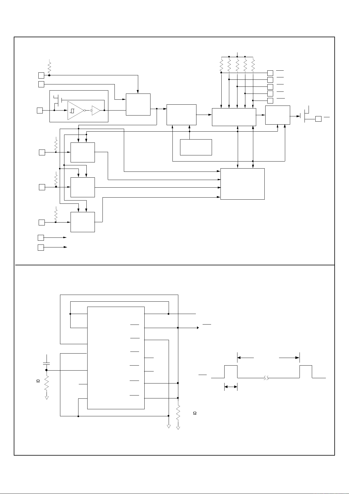
FIGURE 5. LS7210 BLOCK DIAGRAM
14
OUT
+V
+V
+V
+V
+V
-V
VSS
VDD
WB4
WB3
WB2
WB1
WB0
+V
2
NOTE: ÷ 1023 is standard. Any number from 1 to 1022 can be mask programmed.
7210-020298-4
LS7210
B
A
TRIG
CS
OSC
EXT
CLK
VDD
VSS
OUT
WB0
WB1
WB2
WB3
WB4
FIGURE 6. ASYMMETRICAL FLASHER
NOTE: Inputs A, B in Dual-Delay mode. For symmetical flasher tie Pins 8, 9, 10, 11 & 12 to fixed logic level.
8.068 s
323ms
68K
47K
+V
+V
f = 3.17KHz
.005µF
7
6
5
4
2
1
14
13
12
11
10
9
8
3
OUT
OUT
f
 Loading...